Download as PDF, PPTX


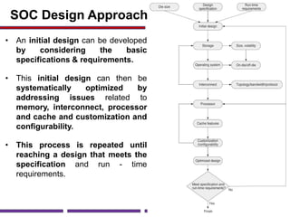


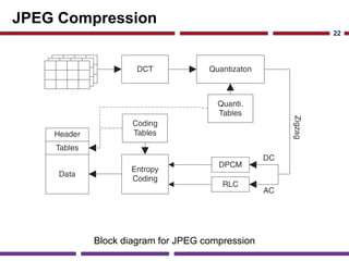
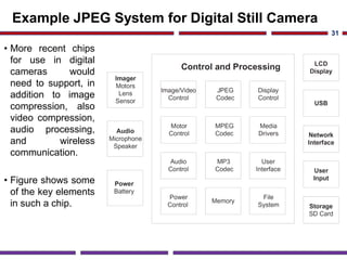

This document discusses application studies of AES encryption and JPEG image compression on SOC designs. It provides an overview of the AES algorithm and requirements, describing the encryption process. An initial SOC design for AES is proposed using an ARM7 processor, and performance is evaluated. JPEG compression is also summarized, outlining the color space transformation, discrete cosine transform, and entropy coding steps. Finally, an example JPEG system for a digital still camera is presented using a TMS320C54x processor to implement the imaging pipeline and compression.