Download as PDF, PPTX


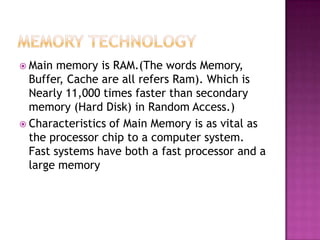
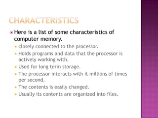


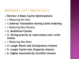
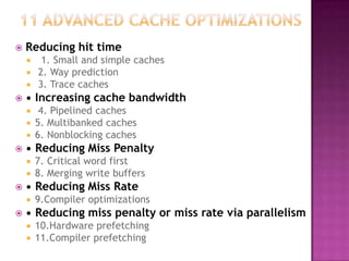
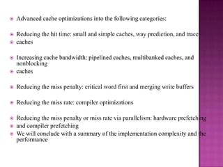
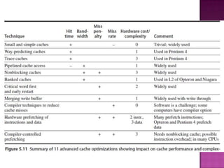
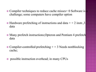
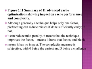


The document discusses various techniques to optimize computer memory performance. It begins by describing the memory hierarchy and characteristics of main memory technologies like SRAM and DRAM. It then discusses 11 advanced cache optimization techniques: 1) Using small, simple caches to reduce hit time. 2) Increasing cache bandwidth through techniques like pipelined, multibanked, and nonblocking caches. 3) Decreasing miss penalty through critical word first and merging write buffers. 4) Reducing miss rate via compiler optimizations and hardware/software prefetching. The document analyzes each technique's impact on performance factors and implementation complexity. Generally, optimizations impact one factor but prefetching can reduce both misses and