Downloaded 410 times


![ARM7-TDMI – Internal Architecture
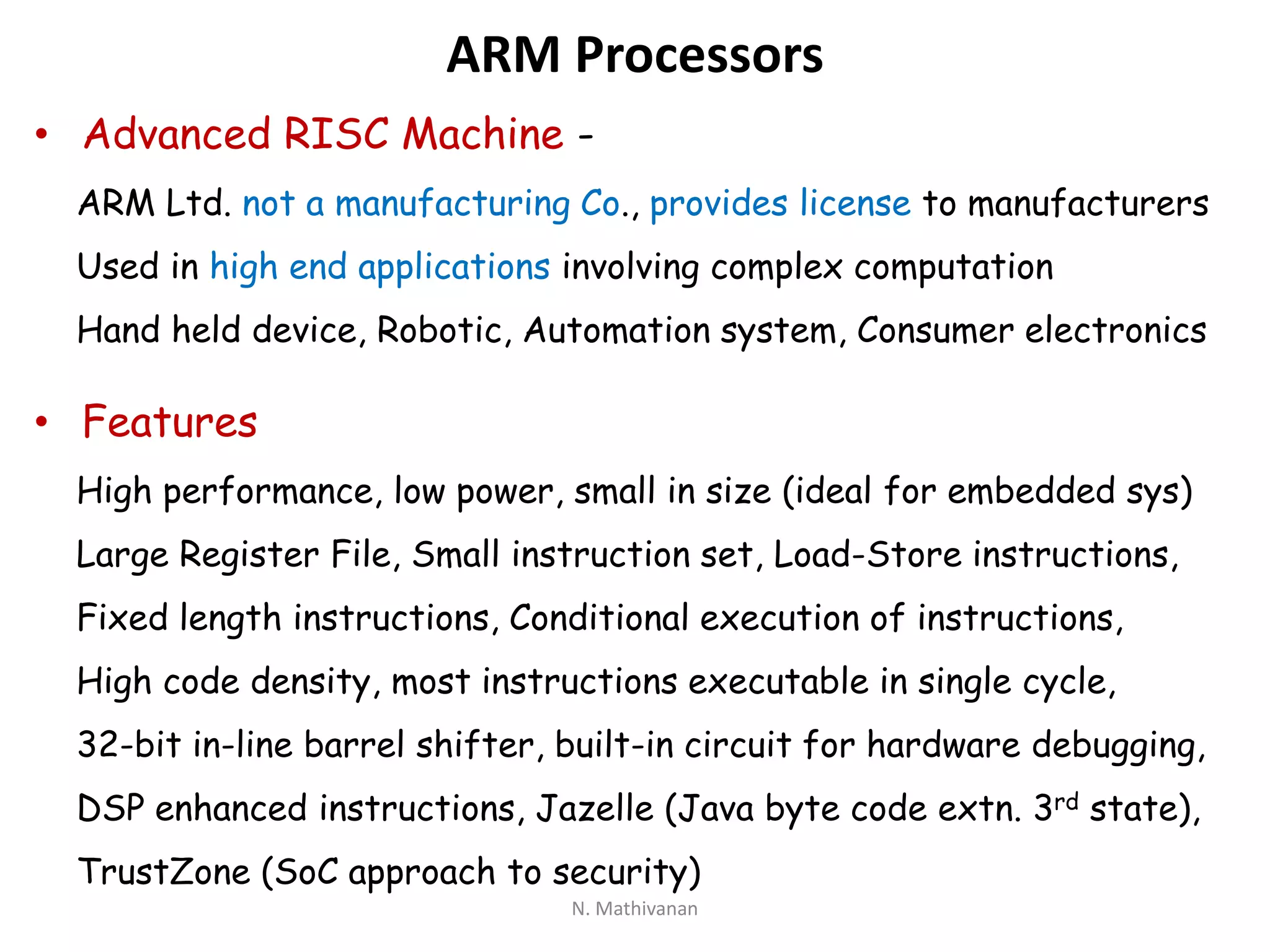
• Von Neumann architecture
• Data bus – 32-bit
• Address bus – 32-bit
Addressable memory space – 4 GB
• Register bank – (31+6) 32-bit regs.
• In-line barrel shifter
• Multiplier
• ALU
• Incrementer
• Address register
• Instruction decoder & control logic
Address Register
Register Bank
(31 x 32-bit registers)
(6 status registers)
Address
Incrementer
32 x 8
Data Bus D[31:0]
A[31:0]
BBus
Data In Register
PCBus
ALUBus
ALU
LogicControl
Barrel Shifter
InstructionDecoderand
Data Out Register
Address Bus
IncrementerBus
ABus
multiplier
N. Mathivanan](https://image.slidesharecdn.com/armprocessors-160404135837/75/ARM-Processors-7-2048.jpg)


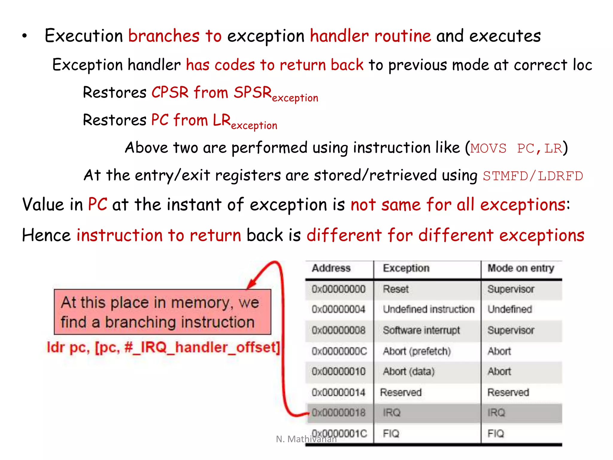

![Except
Exception
Vector
Processor Response to Enter Exception Handler
Return
Instruction
Pri
Reset 0x00000000
SPSR_svc = unexpected
CPSR[4:0]= 10011B (SVC mode)
CPSR[5] = 0 (ARM state), CPSR[6] = 1 (Disable FIQ)
CPSR[7] = 1 (Disable IRQ)
r14_svc = unexpected
PC = 0x00000000 (Exception vector)
No return 1
Un
defined
0x00000004
SPSR_und = CPSR
CPSR[4:0]= 11011B (undefined mode)
CPSR[5] = 0 (ARM state), CPSR[6] unchanged
CPSR[7] = 1 (Disable IRQ)
r14_und = addr of next to undefined instruction
PC = 0x00000004 (Exception vector)
If registers are
not saved in
stack
MOVS pc,lr 6
Registers are saved in stack at entry using:
STMFD sp!,{<reglist>,lr}
If saved:
LDMFD sp!,
{<reglist>,pc}^
N. Mathivanan](https://image.slidesharecdn.com/armprocessors-160404135837/75/ARM-Processors-20-2048.jpg)
![Except
Exception
Vector
Processor Response to Enter Exception Handler
Return
Instruction
Pri
SWI 0x00000008
SPSR_svc = CPSR
CPSR[4:0]= 10011B (SVC mode),
CPSR[5] = 0 (ARM state)
CPSR[6] unchanged, CPSR[7] = 1 (Disable IRQ)
r14_swi = addr of next instruction to SWI
PC = 0x00000008 ;Exception vector
If registers are not
saved in stack
MOVS pc,lr
6
Registers are saved in stack at entry using:
STMFD sp!,{<reglist>,lr}
If saved:
LDMFD sp!,
{<reglist>,pc}^
Prefetch
Abort
0x0000000C
SPSR_abt = CPSR
CPSR[4:0]= 10111B (Abort mode),
CPSR[5] = 0 (ARM state)
CPSR[6] unchanged, CPSR[7] = 1 (Disable IRQ)
r14_abt = aborted instruction addr.+4
PC = 0x0000000C ;Exception vector
If registers are not
saved in stack
SUBS pc,lr,#4
5
Registers are saved in stack at entry using:
SUB lr,lr,#4
STMFD sp!,{<reglist>,lr}
If saved:
LDMFD sp!,
{<reglist>,pc}^
N. Mathivanan](https://image.slidesharecdn.com/armprocessors-160404135837/75/ARM-Processors-21-2048.jpg)
![Exception Exception
Vector
Processor Response to Enter
Exception Handler
Return
Instruction
Pri
Data Abort 0x00000010
SPSR_abt = CPSR
CPSR[4:0]= 10111B (Abort mode),
CPSR[5] = 0 (ARM state) , CPSR[6] unchanged
CPSR[7] = 1 (Disable IRQ)
r14_abt = aborted instruction addr.+8
PC = 0x00000010 (Exception vector)
If registers are
not saved in
stack
SUBS pc,lr,#8 2
Registers are saved in stack at entry using:
SUB lr,lr,#8
STMFD sp!,{<reglist>,lr}
If saved:
LDMFD sp!,
{<reglist>,pc}^
Reserved 0x00000014 Reserved Reserved Reserved
N. Mathivanan](https://image.slidesharecdn.com/armprocessors-160404135837/75/ARM-Processors-22-2048.jpg)
![Except
ion
Exception
Vector
Processor Response to Enter Exception Handler
Return
Instruction
Pri
IRQ 0x00000018
SPSR_irq = CPSR
CPSR[4:0]= 10010B (IRQ mode), CPSR[5] = 0 (ARM state)
CPSR[6] = unchanged, CPSR[7] = 1 (Disable IRQ)
r14_irq = last executed instruction addr.+8
PC = 0x00000018 ;Exception vector
If registers are
not saved in stack
SUBS pc,lr,#4
4
Registers are saved in stack at entry using:
SUB lr,lr,#4
STMFD sp!,{<reglist>,lr}
If saved:
LDMFD sp!,
{<reglist>,pc}^
FIQ 0x0000001C
SPSR_fiq = CPSR
CPSR[4:0]= 10001B (FIQ mode), CPSR[5] = 0 (ARM state)
CPSR[6] = 1 (Disable FIQ), CPSR[7] = 1 (Disable IRQ)
r14_fiq=last executed instruction addr.+8
PC = 0x0000001C ;Exception vector
If registers are
not saved in stack
SUBS pc,lr,#4
3
Registers are saved in stack at entry using:
SUB lr,lr,#4
STMFD sp!,{<reglist>,lr}
If saved:
LDMFD sp!,
{<reglist>,pc}^
N. Mathivanan](https://image.slidesharecdn.com/armprocessors-160404135837/75/ARM-Processors-23-2048.jpg)


![Interface Signals
• Clocks & Timing signals
• Processor mode signals
• Memory interface signals
• Bus control signals
• Interrupts
• Memory management signals
• Coprocessor interface signals
• Debug interface signals
TDO
IR[3:0]
TCK1
SCREG[3:0]
nM[4:0]
A[31:0]
TAPSM[3:0]
nTDOEN
CPB
TBIT
BL[3:0]
ABORT
nOPC
CPA
DIN[31:0]
nMREQ
SEQ
MAS[1:0]
LOCK
D[31:0]
nRW
nTRANS
nCP1
DOUT[31:0]
TCK2
VDD
COMMRX
DBGRQI
ABE
BIGEND
TBE
BUSDIS
RANGEOUT0
BREAKPT
RANGEOUT1
DBGACK
DBGEN
VSS
nENOUT1
nENOUT
nEXEC
nENIN
nHIGHZ
ECAPCLK
ALE
HIGHZ
BUSEN
nRESET
EXTERN0
DBGRQ
EXTERN1
COMMTX
DBE
APE
TMS
TDI
nTRUST
TCK
Bus controls
ECLK
timing
ISYNC
MCLK
Processorstate
Debug
Borndaryscan
Power
Interface
MemoryManagement
nWAIT
MemoryInterface
Coprocessor
nIRQ
nFIQ
Processormode
Clocksand
Boundaryscancontrolsignals
Interface
Interrupts
ARM7-TDMI
N. Mathivanan](https://image.slidesharecdn.com/armprocessors-160404135837/75/ARM-Processors-29-2048.jpg)


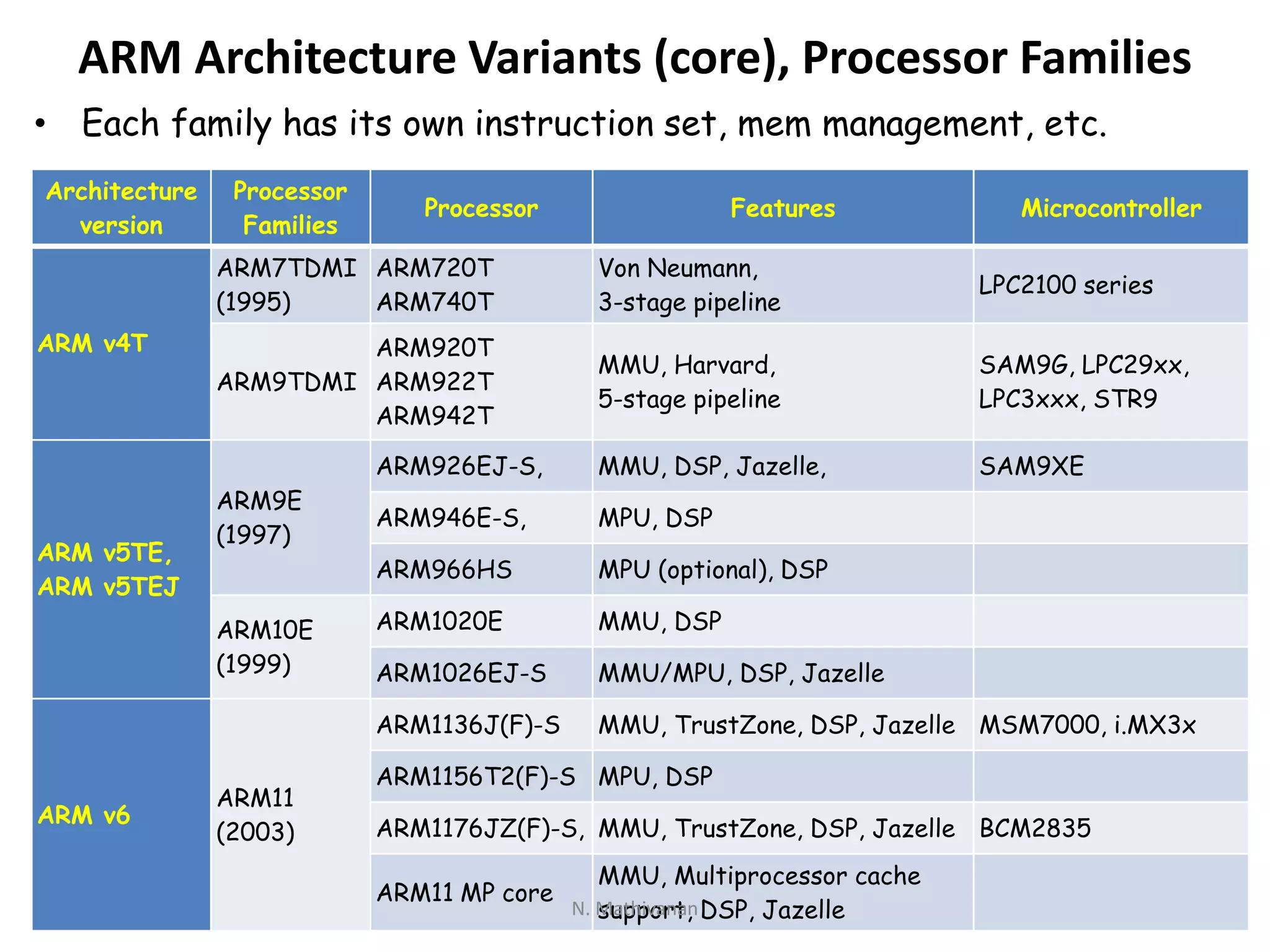
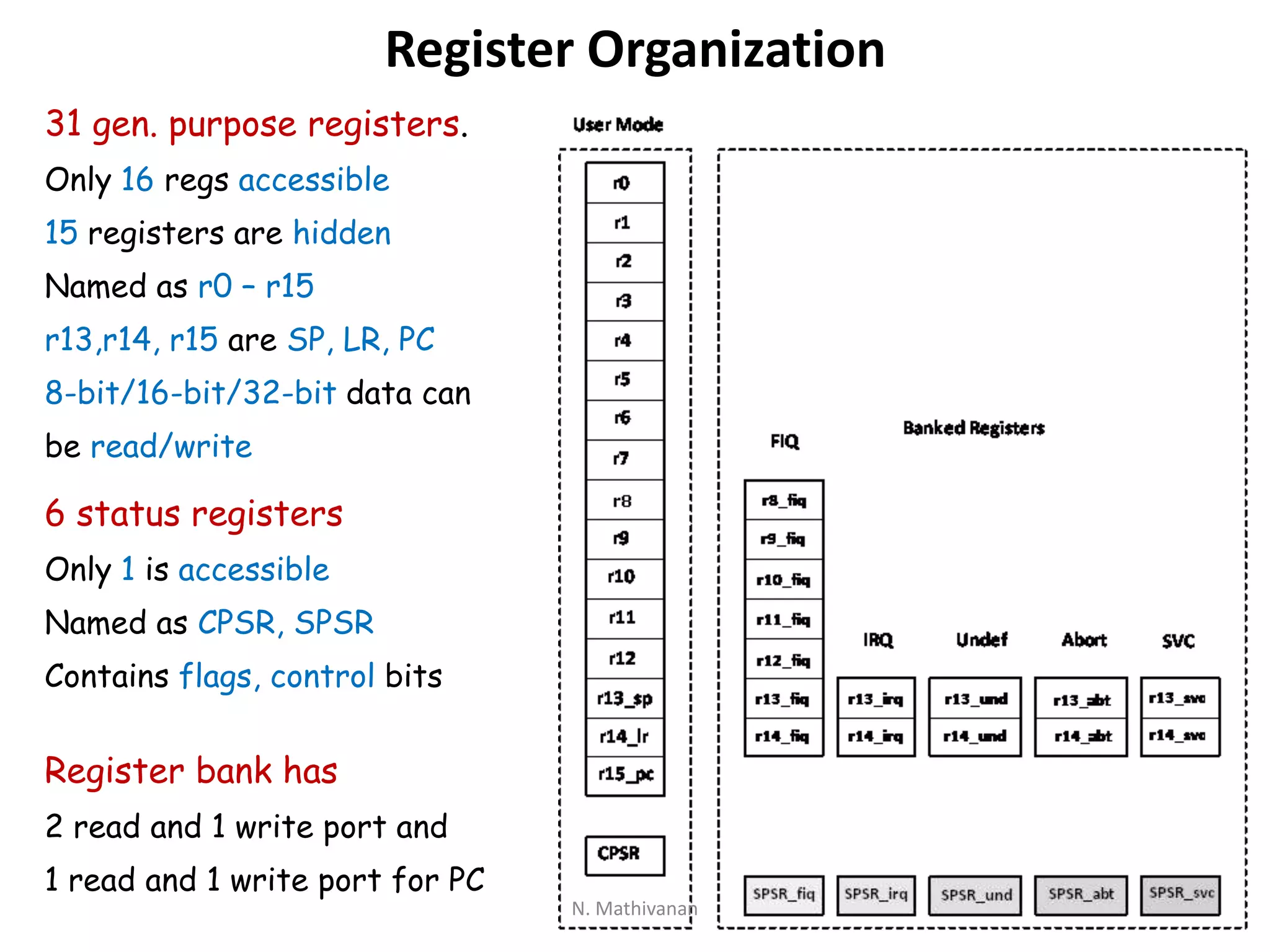
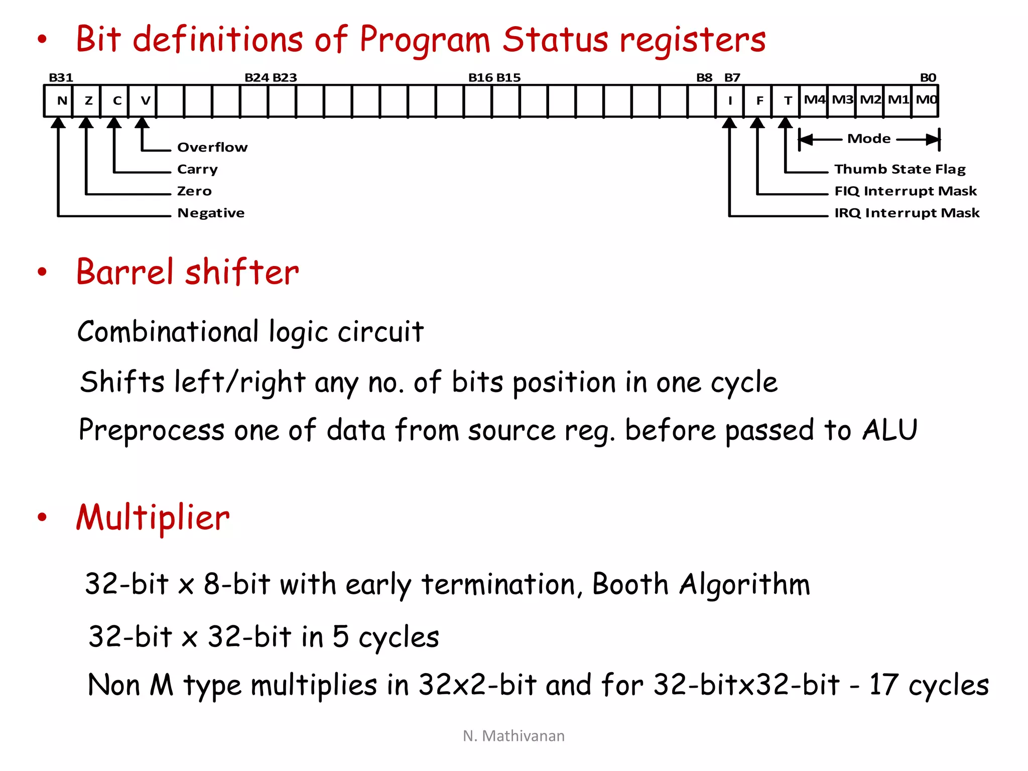
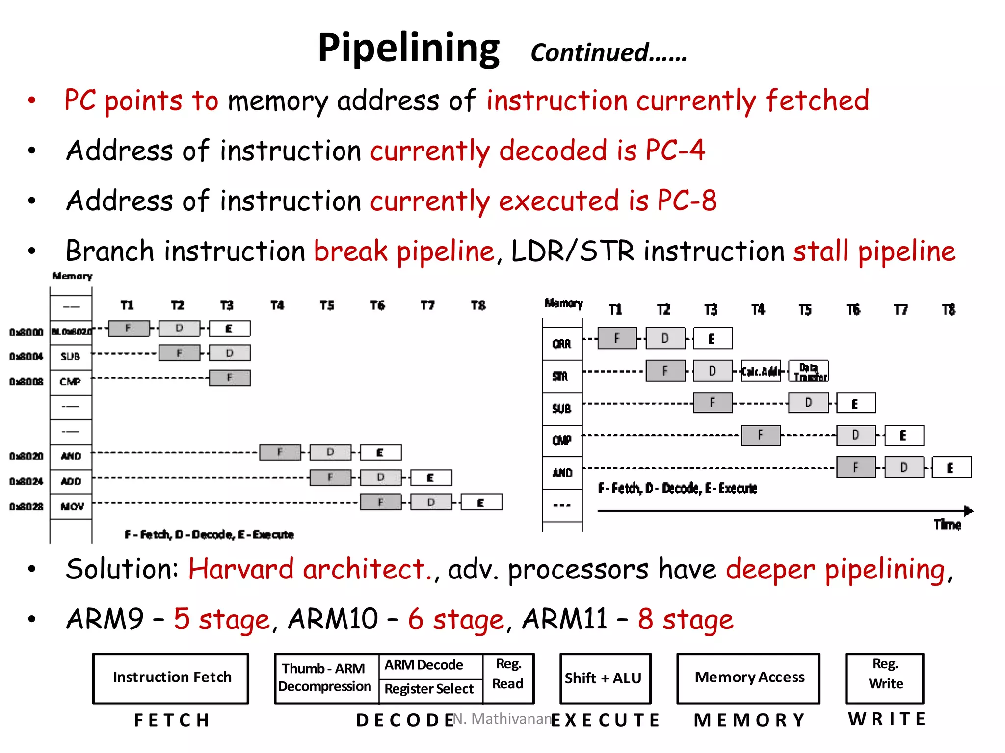
The document provides a detailed overview of ARM processors, their architecture, features, and variants including ARM7-TDMI and multi-core technologies. It covers topics such as instruction sets, register organization, pipelining, operating modes, exception handling, and bus architecture. Additionally, it explains the role of ARM in advanced embedded systems and applications, and highlights various processor families and their specifications.