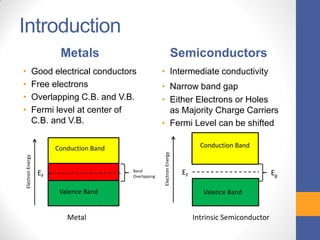
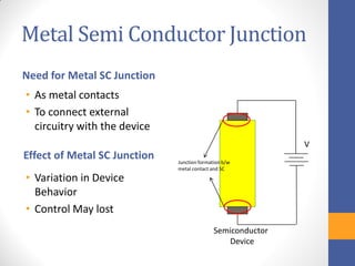
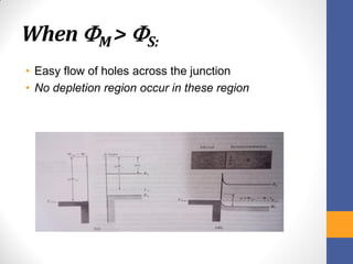
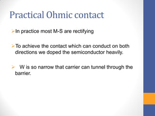
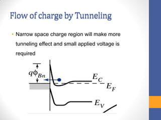
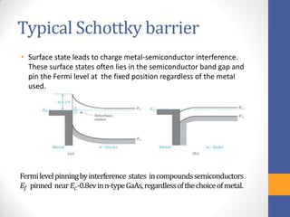
Metal Semi
Conductor Junctions
Agha Muqaddas Ali Khan MESP-1501
Asad Ali MESP-1517
Contents
Introduction
Metals
Semiconductors
Metal Semiconductor Junctions
Schottky Barriers
Rectifying Contacts
Ohmic Contacts
Typical Schottky Barriers
Introduction
Metals
• Good electrical conductors
• Free electrons
• Overlapping C.B. and V.B.
• Fermi level at center of
C.B. and V.B.
Semiconductors
• Intermediate conductivity
• Narrow band gap
• Either Electrons or Holes
as Majority Charge Carriers
• Fermi Level can be shifted
EF
ElectronEnergy
Band
Overlapping
Conduction Band
Valence Band
Metal
ElectronEnergy
Eg
Valence Band
Conduction Band
EF
Intrinsic Semiconductor
Metal Semi Conductor Junction
Need for Metal SC Junction
• As metal contacts
• To connect external
circuitry with the device
Semiconductor
Device
Junction formation b/w
metal contact and SC
Effect of Metal SC Junction
• Variation in Device
Behavior
• Control May lost
V
Schottky Barrier
Metal and N-Type SC
Φ 𝑚 = Work fn. Of Metal
Φ 𝑠 = Work fn. Of SC
Φ 𝑚 > Φ 𝑠
𝑞χ =Electron Affinity
Schottky Barrier
Formation Of Junction
 Fermi level aligning at equilibrium
 Creation of Contact Potential= 𝑉𝑜
 𝑉𝑜 = Φ 𝑚 − Φ 𝑠
 Potential Barrier For electron
injection= Φ 𝐵
 Φ 𝐵 = Φ 𝑚 − χ
 This barrier is called Schottky
Barrier
Schottky Barrier
Metal and P-Type SC
Φ 𝑚 = Work fn. Of Metal
Φ 𝑠 = Work fn. Of SC
Φ 𝑚 < Φ 𝑠
𝑞χ =Electron Affinity
Schottky Barrier
Fermi level aligning at
equilibrium
Creation of Contact
Potential= 𝑉𝑜
𝑉𝑜 = Φ 𝑠 − Φ 𝑚
Potential Barrier For electron
injection= Φ 𝐵
𝑞Φ 𝐵
Formation Of Junction
Rectifying Contacts
• Forward Biasing Schottky
Barrier
• 𝑉𝑜 𝑉𝑜 − 𝑉
• Electron Diff. becomes
easier from SC to M
• Here it is behaving like a
F.B pn junction diode.
F.B. Schottky Barrier
Rectifying Contacts
R.B. Schottky Barrier
• Reverse Biasing Schottky
Barrier
• 𝑽 𝒐 𝑽 𝒐 + 𝑽
• Electron flow from SC to M
becomes Negligible
• Here it is behaving like a R.B
PN junction diode.
• Electron flow from M to SC is
retarded due to barrier
𝜱 𝒎 − 𝝌 in both cases
Rectifying Contacts
• The resulting diode equation of
Schottky diode is similar to that
form of p-n junction.
𝐼 = 𝐼 𝑜(𝑒
𝑞𝑣
𝑘𝑇 − 1)
• Resulting 𝐼 − 𝑉 curve is similar to a
pn junction diode
• In Schottky diode, the reverse
saturation current depends only on
the size of barrier Φ 𝐵
Ohmic Contacts
The current and voltage must be
proportional:
• Having I-V characteristic must be
linear in both direction- Low
Resistance.
• IC contains thousands of P-N which
must be connected or interconnected
for Proper use of Device.
Ideal MS Contact
Assumptions:
• M and S are in intimate
contact, on atomic scale
• No oxides or charges at the
interface
• No intermixing at the
interface
Ohmic MS Contacts
Ways to achieve Ohmic MS contacts
• Reduce the Schottky barrier height. How???
• Reduce the Schottky barrier width (depletion width). How?
How would each approach give us an ohmic contact?
M-S will be Ohmic
• Ohmic contact occur when the induced
charge in the semiconductor during the
fermi level alignment is the Majority
carriers.
When M < S:
• Fermi level aligned at equilibrium by transforming
electrons from metal to semi conductor.
When M < S:
• Barrier for carriers is small
and easily overcome by a
small voltage.
• No depletion region occur in
the semiconductor since
Fermi level calls for
accumulation of majority
carriers in the semi
conductors
• Ohmic contact are formed by
doping the semiconductor
heavily
When M > S:
• Easy flow of holes across the junction
• No depletion region occur in these region
Practical Ohmic contact
In practice most M-S are rectifying
To achieve the contact which can conduct on both
directions we doped the semiconductor heavily.
 W is so narrow that carrier can tunnel through the
barrier.
Flow of charge by Tunneling
• Narrow space charge region will make more
tunneling effect and small applied voltage is
required
Flow of charge by Tunneling
Typical Schottky barrier
• Surface state leads to charge metal-semiconductor interference.
These surface states often lies in the semiconductor band gap and
pin the Fermi level at the fixed position regardless of the metal
used.
Fermilevelpinningbyinterference states incompoundssemiconductors
𝐸𝑓 pinned near 𝐸𝑐-0.8evinn-typeGaAs,regardlessofthechoiceofmetal.

Metal Semi-Conductor Junctions

  • 1.
    Metal Semi Conductor Junctions AghaMuqaddas Ali Khan MESP-1501 Asad Ali MESP-1517
  • 2.
    Contents Introduction Metals Semiconductors Metal Semiconductor Junctions SchottkyBarriers Rectifying Contacts Ohmic Contacts Typical Schottky Barriers
  • 3.
    Introduction Metals • Good electricalconductors • Free electrons • Overlapping C.B. and V.B. • Fermi level at center of C.B. and V.B. Semiconductors • Intermediate conductivity • Narrow band gap • Either Electrons or Holes as Majority Charge Carriers • Fermi Level can be shifted EF ElectronEnergy Band Overlapping Conduction Band Valence Band Metal ElectronEnergy Eg Valence Band Conduction Band EF Intrinsic Semiconductor
  • 4.
    Metal Semi ConductorJunction Need for Metal SC Junction • As metal contacts • To connect external circuitry with the device Semiconductor Device Junction formation b/w metal contact and SC Effect of Metal SC Junction • Variation in Device Behavior • Control May lost V
  • 5.
    Schottky Barrier Metal andN-Type SC Φ 𝑚 = Work fn. Of Metal Φ 𝑠 = Work fn. Of SC Φ 𝑚 > Φ 𝑠 𝑞χ =Electron Affinity
  • 6.
    Schottky Barrier Formation OfJunction  Fermi level aligning at equilibrium  Creation of Contact Potential= 𝑉𝑜  𝑉𝑜 = Φ 𝑚 − Φ 𝑠  Potential Barrier For electron injection= Φ 𝐵  Φ 𝐵 = Φ 𝑚 − χ  This barrier is called Schottky Barrier
  • 7.
    Schottky Barrier Metal andP-Type SC Φ 𝑚 = Work fn. Of Metal Φ 𝑠 = Work fn. Of SC Φ 𝑚 < Φ 𝑠 𝑞χ =Electron Affinity
  • 8.
    Schottky Barrier Fermi levelaligning at equilibrium Creation of Contact Potential= 𝑉𝑜 𝑉𝑜 = Φ 𝑠 − Φ 𝑚 Potential Barrier For electron injection= Φ 𝐵 𝑞Φ 𝐵 Formation Of Junction
  • 9.
    Rectifying Contacts • ForwardBiasing Schottky Barrier • 𝑉𝑜 𝑉𝑜 − 𝑉 • Electron Diff. becomes easier from SC to M • Here it is behaving like a F.B pn junction diode. F.B. Schottky Barrier
  • 10.
    Rectifying Contacts R.B. SchottkyBarrier • Reverse Biasing Schottky Barrier • 𝑽 𝒐 𝑽 𝒐 + 𝑽 • Electron flow from SC to M becomes Negligible • Here it is behaving like a R.B PN junction diode. • Electron flow from M to SC is retarded due to barrier 𝜱 𝒎 − 𝝌 in both cases
  • 11.
    Rectifying Contacts • Theresulting diode equation of Schottky diode is similar to that form of p-n junction. 𝐼 = 𝐼 𝑜(𝑒 𝑞𝑣 𝑘𝑇 − 1) • Resulting 𝐼 − 𝑉 curve is similar to a pn junction diode • In Schottky diode, the reverse saturation current depends only on the size of barrier Φ 𝐵
  • 12.
    Ohmic Contacts The currentand voltage must be proportional: • Having I-V characteristic must be linear in both direction- Low Resistance. • IC contains thousands of P-N which must be connected or interconnected for Proper use of Device.
  • 13.
    Ideal MS Contact Assumptions: •M and S are in intimate contact, on atomic scale • No oxides or charges at the interface • No intermixing at the interface
  • 14.
    Ohmic MS Contacts Waysto achieve Ohmic MS contacts • Reduce the Schottky barrier height. How??? • Reduce the Schottky barrier width (depletion width). How? How would each approach give us an ohmic contact?
  • 15.
    M-S will beOhmic • Ohmic contact occur when the induced charge in the semiconductor during the fermi level alignment is the Majority carriers.
  • 16.
    When M <S: • Fermi level aligned at equilibrium by transforming electrons from metal to semi conductor.
  • 17.
    When M <S: • Barrier for carriers is small and easily overcome by a small voltage. • No depletion region occur in the semiconductor since Fermi level calls for accumulation of majority carriers in the semi conductors • Ohmic contact are formed by doping the semiconductor heavily
  • 18.
    When M >S: • Easy flow of holes across the junction • No depletion region occur in these region
  • 19.
    Practical Ohmic contact Inpractice most M-S are rectifying To achieve the contact which can conduct on both directions we doped the semiconductor heavily.  W is so narrow that carrier can tunnel through the barrier.
  • 20.
    Flow of chargeby Tunneling • Narrow space charge region will make more tunneling effect and small applied voltage is required Flow of charge by Tunneling
  • 21.
    Typical Schottky barrier •Surface state leads to charge metal-semiconductor interference. These surface states often lies in the semiconductor band gap and pin the Fermi level at the fixed position regardless of the metal used. Fermilevelpinningbyinterference states incompoundssemiconductors 𝐸𝑓 pinned near 𝐸𝑐-0.8evinn-typeGaAs,regardlessofthechoiceofmetal.