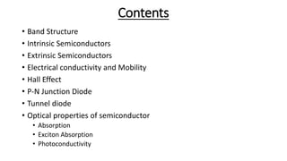
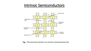
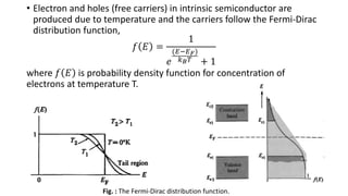
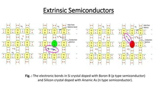
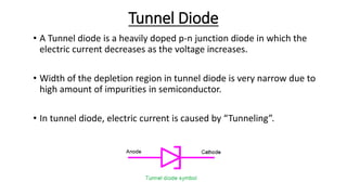
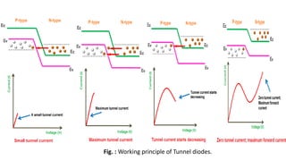
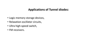
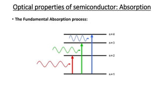
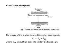
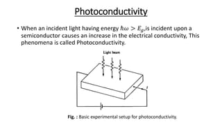
Basic of
Semiconductors and
Optical Properties
- Kamran Ansari
CBS 6th Semester09 – May - 2018
Contents
• Band Structure
• Intrinsic Semiconductors
• Extrinsic Semiconductors
• Electrical conductivity and Mobility
• Hall Effect
• P-N Junction Diode
• Tunnel diode
• Optical properties of semiconductor
• Absorption
• Exciton Absorption
• Photoconductivity
Band Structure
The energy of the conduction band has the form:
𝐸𝑐 = 𝐸𝑔 +
ℏ2
𝑘2
2𝑚 𝑒
Intrinsic Semiconductors
Fig. : The electronic bonds in an intrinsic semiconductor (Si).
• Electron and holes (free carriers) in intrinsic semiconductor are
produced due to temperature and the carriers follow the Fermi-Dirac
distribution function,
𝑓 𝐸 =
1
𝑒
(𝐸−𝐸 𝐹)
𝑘 𝐵 𝑇 + 1
where 𝑓 𝐸 is probability density function for concentration of
electrons at temperature T.
Fig. : The Fermi-Dirac distribution function.
Extrinsic Semiconductors
Fig. : The electronic bonds in Si crystal doped with Boron B (p type semiconductor)
and Silicon crystal doped with Arsenic As (n type semiconductor).
Electrical conductivity and Mobility
• Electrical conductivity is the measure of a material's ability to allow
the transport of an electric charge.
𝜎𝑒 =
𝑛𝑒2
𝜏 𝑒
𝑚 𝑒
𝜎𝑒 ≅ 1 𝞨𝑚 −1is a typical figure in semiconductor.
• The electron mobility 𝜇 𝑒is the drift velocity electron per unit field
strength and measure of the rapidity or swiftness of the motion of
electron in the field.
𝜇 𝑒 =
𝑒𝜏 𝑒
𝑚 𝑒
Hall Effect
The Hall effect is the production of a voltage difference (the Hall voltage) across
an electrical conductor, transverse to an electric current in the conductor and to
an applied magnetic field perpendicular to the current.
Hall voltage 𝑉𝐻 =
𝐼 𝑥 𝐵 𝑧
𝑛𝑡𝑒
Hall coefficient 𝑅 𝐻 =
𝐸 𝐻
𝐽 𝑥 𝐵 𝑧
= −
1
𝑛𝑒
Applications of Hall effect:
• The sign of charge carriers,
• The number of charge carriers per unit volume,
• Mobility of charge carriers,
• The unknown magnetic field if the hall voltage (VH) is known.
P-N Junction Diode
• Shockley Diode equation,
𝐼 = 𝐼𝑠 𝑒
𝑉 𝐷
𝑛𝑉 𝑇−1
I : diode current,
𝐼𝑠: reverse bias saturation current,
𝑉𝐷:voltage across the diode,
𝑉𝑇:thermal voltage kT/q = 25.85mV at 300K and,
𝑛 : ideality factor (between 1 and 2)
Tunnel Diode
• A Tunnel diode is a heavily doped p-n junction diode in which the
electric current decreases as the voltage increases.
• Width of the depletion region in tunnel diode is very narrow due to
high amount of impurities in semiconductor.
• In tunnel diode, electric current is caused by “Tunneling”.
Fig. : Working principle of Tunnel diodes.
Applications of Tunnel diodes:
• Logic memory storage devices,
• Relaxation oscillator circuits,
• Ultra high-speed switch,
• FM receivers.
Optical properties of semiconductor: Absorption
• The Fundamental Absorption process:
• The Exciton absorption:
The energy of the photon involved in exciton absorption is
ℎ𝜗 = 𝐸𝑔 − 𝐸𝑒𝑥
where 𝐸𝑒𝑥 (about 0.01 eV)is the exciton binding energy.
Fig. : The exciton level and associated absorption.
Photoconductivity
• When an incident light having energy ℏ𝜔 > 𝐸𝑔,is incident upon a
semiconductor causes an increase in the electrical conductivity, This
phenomena is called Photoconductivity.
Fig. : Basic experimental setup for photoconductivity.
Thank You

Basic of semiconductors and optical properties

  • 1.
    Basic of Semiconductors and OpticalProperties - Kamran Ansari CBS 6th Semester09 – May - 2018
  • 2.
    Contents • Band Structure •Intrinsic Semiconductors • Extrinsic Semiconductors • Electrical conductivity and Mobility • Hall Effect • P-N Junction Diode • Tunnel diode • Optical properties of semiconductor • Absorption • Exciton Absorption • Photoconductivity
  • 3.
    Band Structure The energyof the conduction band has the form: 𝐸𝑐 = 𝐸𝑔 + ℏ2 𝑘2 2𝑚 𝑒
  • 4.
    Intrinsic Semiconductors Fig. :The electronic bonds in an intrinsic semiconductor (Si).
  • 5.
    • Electron andholes (free carriers) in intrinsic semiconductor are produced due to temperature and the carriers follow the Fermi-Dirac distribution function, 𝑓 𝐸 = 1 𝑒 (𝐸−𝐸 𝐹) 𝑘 𝐵 𝑇 + 1 where 𝑓 𝐸 is probability density function for concentration of electrons at temperature T. Fig. : The Fermi-Dirac distribution function.
  • 6.
    Extrinsic Semiconductors Fig. :The electronic bonds in Si crystal doped with Boron B (p type semiconductor) and Silicon crystal doped with Arsenic As (n type semiconductor).
  • 7.
    Electrical conductivity andMobility • Electrical conductivity is the measure of a material's ability to allow the transport of an electric charge. 𝜎𝑒 = 𝑛𝑒2 𝜏 𝑒 𝑚 𝑒 𝜎𝑒 ≅ 1 𝞨𝑚 −1is a typical figure in semiconductor. • The electron mobility 𝜇 𝑒is the drift velocity electron per unit field strength and measure of the rapidity or swiftness of the motion of electron in the field. 𝜇 𝑒 = 𝑒𝜏 𝑒 𝑚 𝑒
  • 8.
    Hall Effect The Halleffect is the production of a voltage difference (the Hall voltage) across an electrical conductor, transverse to an electric current in the conductor and to an applied magnetic field perpendicular to the current. Hall voltage 𝑉𝐻 = 𝐼 𝑥 𝐵 𝑧 𝑛𝑡𝑒 Hall coefficient 𝑅 𝐻 = 𝐸 𝐻 𝐽 𝑥 𝐵 𝑧 = − 1 𝑛𝑒
  • 9.
    Applications of Halleffect: • The sign of charge carriers, • The number of charge carriers per unit volume, • Mobility of charge carriers, • The unknown magnetic field if the hall voltage (VH) is known.
  • 10.
  • 11.
    • Shockley Diodeequation, 𝐼 = 𝐼𝑠 𝑒 𝑉 𝐷 𝑛𝑉 𝑇−1 I : diode current, 𝐼𝑠: reverse bias saturation current, 𝑉𝐷:voltage across the diode, 𝑉𝑇:thermal voltage kT/q = 25.85mV at 300K and, 𝑛 : ideality factor (between 1 and 2)
  • 12.
    Tunnel Diode • ATunnel diode is a heavily doped p-n junction diode in which the electric current decreases as the voltage increases. • Width of the depletion region in tunnel diode is very narrow due to high amount of impurities in semiconductor. • In tunnel diode, electric current is caused by “Tunneling”.
  • 13.
    Fig. : Workingprinciple of Tunnel diodes.
  • 14.
    Applications of Tunneldiodes: • Logic memory storage devices, • Relaxation oscillator circuits, • Ultra high-speed switch, • FM receivers.
  • 15.
    Optical properties ofsemiconductor: Absorption • The Fundamental Absorption process:
  • 16.
    • The Excitonabsorption: The energy of the photon involved in exciton absorption is ℎ𝜗 = 𝐸𝑔 − 𝐸𝑒𝑥 where 𝐸𝑒𝑥 (about 0.01 eV)is the exciton binding energy. Fig. : The exciton level and associated absorption.
  • 17.
    Photoconductivity • When anincident light having energy ℏ𝜔 > 𝐸𝑔,is incident upon a semiconductor causes an increase in the electrical conductivity, This phenomena is called Photoconductivity. Fig. : Basic experimental setup for photoconductivity.
  • 18.