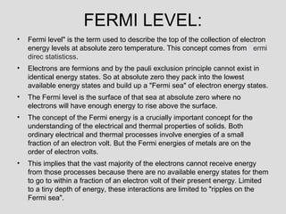
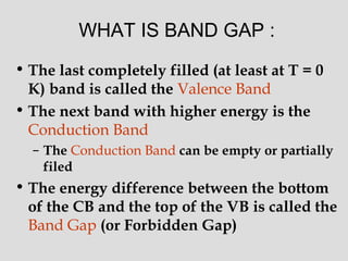
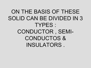
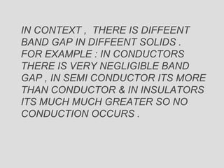
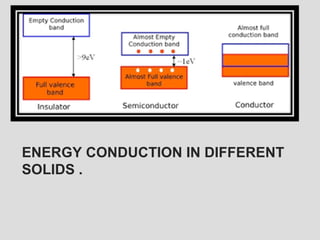
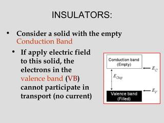
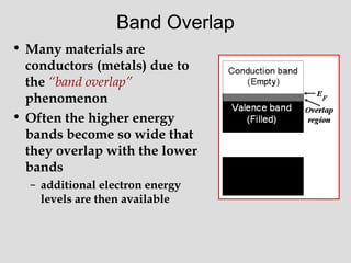
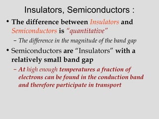
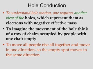
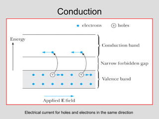
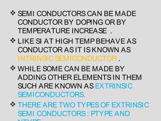
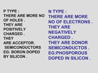
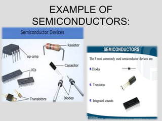
The document discusses band theory of solids and key concepts like the Fermi level, band gaps, and conduction in different materials. It explains that the Fermi level describes the highest occupied electron energy level at absolute zero. Materials are classified based on their band gap as conductors, semiconductors, or insulators. Conductors have a small or overlapping band gap allowing conduction, while insulators have a large gap preventing conduction except at very high temperatures. Semiconductors have an intermediate gap size and can conduct at higher temperatures when electrons are thermally excited across the gap.

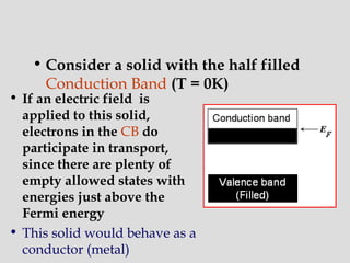
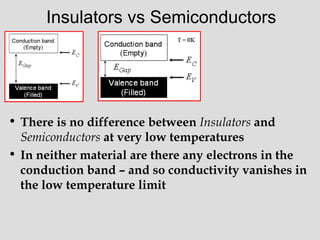
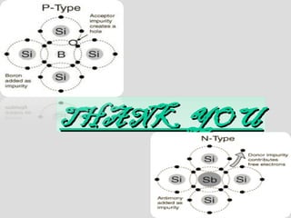
![• The electrons in the VB do not
participate in the current,
since
– Classically, electrons in the electric
field accelerate, so they acquire
[kinetic] energy
– In QM this means they must
acquire slightly higher energy
and jump to another quantum
state
– Such states must be available, i.e.
empty allowed states
– But no such state are available in the
This solid
would behave
as an insulator](https://image.slidesharecdn.com/bandtheory-190408151124/85/Band-theory-10-320.jpg)


![谷歌留痕技术 [ 𝙩𝙤𝙥 𝟮𝟯𝟯. 𝙘 𝙤𝙢 ]](https://cdn.slidesharecdn.com/ss_thumbnails/top233-260130174328-3833018c-thumbnail.jpg?width=640&height=640&fit=bounds)


