The document discusses energy bands in semiconductors. It explains that semiconductors have a valence band, conduction band, and a forbidden energy gap between the bands. Intrinsic semiconductors generate electron-hole pairs when heated, while extrinsic semiconductors are doped with impurities to generate more charge carriers. P-type semiconductors are doped with acceptors to generate holes, while N-type are doped with donors to generate electrons. A PN junction forms a depletion region that acts as a diode, allowing current in one direction but blocking it in the other. Semiconductors find applications in devices like transistors, solar cells, and LEDs.
Energy bands consisting of a large number of closely spaced energy levels exist in crystalline materials. The bands can be thought of as the collection of the individual energy levels of electrons surrounding each atom. The wavefunctions of the individual electrons, however, overlap with those of electrons confined to neighboring atoms. The Pauli exclusion principle does not allow the electron energy levels to be the same so that one obtains a set of closely spaced energy levels, forming an energy band. The energy band model is crucial to any detailed treatment of semiconductor devices. It provides the framework needed to understand the concept of an energy bandgap and that of conduction in an almost filled band as described by the empty states.
BASIC ELECTRONICS
Electronics is a branch of physics that deals with the emission and effects of electrons in materials.
Or
Is a branch of science dealing with the study and development of circuit involving semi conductors, logic gates and other electrical components like resistors, capacitors and inductors.
Electronics and Communication Engineering is the Branch of Engineering. Electronics and Communication Engineering field requires an understanding of core areas including Engineering Graphics, Computer Programming,Electronics Devices and Circuits-I, Network Analysis, Signals and Systems, Communication Systems, Electromagnetics Engineering, Digital Signal Processing, Embedded Systems, Microprocessor and Computer Architecture. Ekeeda offers Online Mechanical Engineering Courses for all the Subjects as per the Syllabus. Visit : https://ekeeda.com/streamdetails/stream/Electronics-and-Communication-Engineering
We all have good and bad thoughts from time to time and situation to situation. We are bombarded daily with spiraling thoughts(both negative and positive) creating all-consuming feel , making us difficult to manage with associated suffering. Good thoughts are like our Mob Signal (Positive thought) amidst noise(negative thought) in the atmosphere. Negative thoughts like noise outweigh positive thoughts. These thoughts often create unwanted confusion, trouble, stress and frustration in our mind as well as chaos in our physical world. Negative thoughts are also known as “distorted thinking”.
Read| The latest issue of The Challenger is here! We are thrilled to announce that our school paper has qualified for the NATIONAL SCHOOLS PRESS CONFERENCE (NSPC) 2024. Thank you for your unwavering support and trust. Dive into the stories that made us stand out!
Students, digital devices and success - Andreas Schleicher - 27 May 2024..pptxEduSkills OECD
Andreas Schleicher presents at the OECD webinar ‘Digital devices in schools: detrimental distraction or secret to success?’ on 27 May 2024. The presentation was based on findings from PISA 2022 results and the webinar helped launch the PISA in Focus ‘Managing screen time: How to protect and equip students against distraction’ https://www.oecd-ilibrary.org/education/managing-screen-time_7c225af4-en and the OECD Education Policy Perspective ‘Students, digital devices and success’ can be found here - https://oe.cd/il/5yV
The Roman Empire A Historical Colossus.pdfkaushalkr1407
The Roman Empire, a vast and enduring power, stands as one of history's most remarkable civilizations, leaving an indelible imprint on the world. It emerged from the Roman Republic, transitioning into an imperial powerhouse under the leadership of Augustus Caesar in 27 BCE. This transformation marked the beginning of an era defined by unprecedented territorial expansion, architectural marvels, and profound cultural influence.
The empire's roots lie in the city of Rome, founded, according to legend, by Romulus in 753 BCE. Over centuries, Rome evolved from a small settlement to a formidable republic, characterized by a complex political system with elected officials and checks on power. However, internal strife, class conflicts, and military ambitions paved the way for the end of the Republic. Julius Caesar’s dictatorship and subsequent assassination in 44 BCE created a power vacuum, leading to a civil war. Octavian, later Augustus, emerged victorious, heralding the Roman Empire’s birth.
Under Augustus, the empire experienced the Pax Romana, a 200-year period of relative peace and stability. Augustus reformed the military, established efficient administrative systems, and initiated grand construction projects. The empire's borders expanded, encompassing territories from Britain to Egypt and from Spain to the Euphrates. Roman legions, renowned for their discipline and engineering prowess, secured and maintained these vast territories, building roads, fortifications, and cities that facilitated control and integration.
The Roman Empire’s society was hierarchical, with a rigid class system. At the top were the patricians, wealthy elites who held significant political power. Below them were the plebeians, free citizens with limited political influence, and the vast numbers of slaves who formed the backbone of the economy. The family unit was central, governed by the paterfamilias, the male head who held absolute authority.
Culturally, the Romans were eclectic, absorbing and adapting elements from the civilizations they encountered, particularly the Greeks. Roman art, literature, and philosophy reflected this synthesis, creating a rich cultural tapestry. Latin, the Roman language, became the lingua franca of the Western world, influencing numerous modern languages.
Roman architecture and engineering achievements were monumental. They perfected the arch, vault, and dome, constructing enduring structures like the Colosseum, Pantheon, and aqueducts. These engineering marvels not only showcased Roman ingenuity but also served practical purposes, from public entertainment to water supply.
Welcome to TechSoup New Member Orientation and Q&A (May 2024).pdfTechSoup
In this webinar you will learn how your organization can access TechSoup's wide variety of product discount and donation programs. From hardware to software, we'll give you a tour of the tools available to help your nonprofit with productivity, collaboration, financial management, donor tracking, security, and more.
The Art Pastor's Guide to Sabbath | Steve ThomasonSteve Thomason
What is the purpose of the Sabbath Law in the Torah. It is interesting to compare how the context of the law shifts from Exodus to Deuteronomy. Who gets to rest, and why?
How to Create Map Views in the Odoo 17 ERPCeline George
The map views are useful for providing a geographical representation of data. They allow users to visualize and analyze the data in a more intuitive manner.
Ethnobotany and Ethnopharmacology:
Ethnobotany in herbal drug evaluation,
Impact of Ethnobotany in traditional medicine,
New development in herbals,
Bio-prospecting tools for drug discovery,
Role of Ethnopharmacology in drug evaluation,
Reverse Pharmacology.
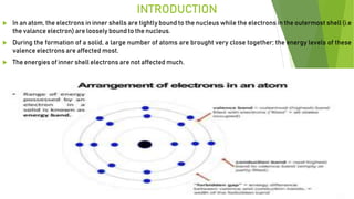
1. INTRODUCTION
In an atom, the electrons in inner shells are tightly bound to the nucleus while the electrons in the outermost shell (i.e
the valance electron) are loosely bound to the nucleus.
During the formation of a solid, a large number of atoms are brought very close together; the energy levels of these
valence electrons are affected most.
The energies of inner shell electrons are not affected much.
2. ENERGY BAND : It is the range of energies that an electron may possess in an atom.
TYPES OF ENERGY BAND:
a) Valence Band b) Conduction Band c) Forbidden Energy Gap Band
VALENCE BAND
The valence electrons contain a series of energy levels and form an energy band known as the valence band.
The valence band is the band, which has the highest occupied energy.
It may be completely filled or partially filled with electrons
CONDUCTION BAND
The valence electrons are so loosely attached to the nucleus that even at room temperature, few of the valence
electrons leave the band to be free.
These are called as free electrons as they tend to move towards the neighboring atoms.
These free electrons are the ones which conduct the current in a conductor and hence called as Conduction Electrons
and they can move freely in the conduction band
The band which contains conduction electrons is called as Conduction Band. The conduction band is the band having
the lowest occupied energy.
3. FORBIDDEN BAND
The gap between valence band and conduction band is called as forbidden energy gap.
As the name implies, this band is the forbidden one without energy. Hence no electron stays in this band. The valence
electrons, while going to the conduction band, pass through this.
The forbidden energy gap if greater, means that the valence band electrons are tightly bound to the nucleus. Now, in
order to push the electrons out of the valence band, some external energy is required, which would be equal to the
forbidden energy gap.
It is denoted by Eg and is the amount of energy to be supplied to the electron in VB to get excited into the CB.
When an electron gains sufficient energy, it is ejected from the valence band.
Because of this, a covalent bond is broken and a vacancy for electron, called Hole, is generated.
It is supposed to behave as a positive charge.
This Hole can travel to the adjacent atom by acquiring an electron from an atom.
When an electron is captured by a Hole, the covalent bond is again reestablished.
Based on the size of the forbidden energy gap, the CONDUCTORS, SEMICONDUCTORS, AND INSULATORS are formed.
The figure given below shows the conduction band, valence band, and the forbidden energy gap
4.
5. CONDUCTORS
Conductors are the
substances or materials
that conduct electricity as
they allow electricity to flow
through them.
The forbidden energy gap
disappears in the
conductors, as the
conduction band and the
valence band come close to
each other and overlap.
Copper, gold, and silver are
a few examples of
conductors.
In conductors large number
of free electrons are
available for the conduction
and No concept of hole
formation is there because
the continuous flow of
electrons contributes to the
current produced.
INSULATORS
Insulators are the substances or materials that don't conduct electricity as they
don't allow electricity to flow through them.
The forbidden energy gap in the insulators is large enough due to which the
conduction of electricity can't take place.
Rubber and wood are a few examples of insulators.
SEMICONDUCTORS
Semiconductors are substances or materials having conductivity between the
conductors and the insulators.
In semiconductors, the forbidden energy gap is small, and the conduction of
electricity will take place only if we apply some external energy.
Germanium and silicon are a few examples of semiconductors. The figure given
below shows the structure of energy bands in semiconductors.
For Germanium (Ge), the value of the forbidden energy gap is 0.7eV, and for Silicon
(Si), it is 1.1eV.
PROPERTIES OF SEMICONDUCTOR:
Their resistivity is higher than conductors but lesser than insulators
Resistance decrease with increase in temperature
8. GENERATION OF HOLES & ELECTRONS
At very low temperature all the valence electrons are tightly
held by parent atoms and covalent bond by other atoms.
Since the electrons are not able to move freely in crystal
structure they cannot conduct electricity.
Assume when the temperature increases, the covalent bond
breaks and the electron involved in the bonding departs from
them as free electron.
This free electron is free to move anywhere within the structure.
The vacancy left by the free electron which results in
incompletionof covalent bond is called holes.
This electron –hole pair act as carrier in electricity.
The energy required to break a covalent bond in a
semiconductoris known as energy gap.
The value of Eg at room temperature for Ge is 0.72eV and Si is
1.1eV.
9. MECHANISM OF HOLES CONTRIBUTING TO CONDUCTIVITY
A hole is a positive charge which has
equal magnitude but opposite direction
to electronic charge.
This electron-hole pair is called charge
carrier.
Thus in a semiconductor the flow of
current is due to movement of free
electrons in one direction and holes in
opposite direction.
10. EXTRINSIC SEMICONDUCTOR
The process of adding impurities to intrinsic semiconductor is termed as doping and
resulting semiconductors are called impure or extrinsic semiconductor.
The impurities added, are generally pentavalent and trivalent impurities.
The purpose of adding impurity is to jncrease either the number of free electrons or
holes in a semiconductor.
Generally two types of impurity atoms are added to the semiconductor namely, the
impurity atoms containing 5 valence electrons (penta valent impurity) and 3 valence
electrons (tri-valent impurity).
Depending upon the type of impurity atoms added to semiconductor the resulting
extrinsic semiconductor are of two types
N-type Semiconductor
P-type Semiconductor
11. N-Type Semiconductor
• Semiconductors which are obtained by
introducing pentavalent impurity .
• The elements in this group contain 5
valence electrons.
• Eg: P, Sb, As,Bi
• These elements donate excess electron
carriers,
• Thus ,after donation the impurity atom
becomes positively charged ion known as
donor ion.
• Therefore , such elements are known as
donor or N-type impurities.
• In an N-type the current flows due to the
movement of electrons and holes.
• But as major part of the current flow is due
to electrons,in n-type semiconductor
electrons are majority carriers and holes
are minority carriers
12. P-Type Semiconductor
• Semiconductors which are obtained by
introducing trivalent impurity.
• The elements in this group contain 3
valence electrons.
• Eg: Ga, In, Al,B
• These elements accepts electron
because of availability of positive charge
carriers(holes)
• Thus ,after accepting the impurity atom
becomes negatively charged ion known
as acceptor ion.
• In an P-type the current flows due to the
movement of electrons and holes.
• But as major part of the current flow is
due to holes,in P-type semiconductor
holes are majority carriers while
electrons are minority carriers
14. MOBILE CHARGE CARRIERS AND IMMOBILE IONS
Mobile charge carriers are those
which take part in conduction
while immobile ions are those
which do not take part in
conduction.
In N-type Semiconductor donor
ions are immobile ions and
electrons are mobile charge
carriers.
In P-type Semiconductor
acceptor ions are immobile ions
and holes are mobile charge
carriers.
15. PN JUNCTION
P-n junctions are formed by joining n-type and p-type
semiconductor materials.
When a voltage is applied to a semiconductor ,the
electrons will move towards positive terminal of battery
while holes moves towards the negative terminal of
battery.
This movement of holes and electrons will constitute a
current known as DRIFT CURRENT.
Semiconductor will exhibit a current in the absence of
voltage.
This is achieved due concentration gradient exists in the
semiconductor material, and the process is known as
diffusion.
Since in a semiconductor the n-type region has a high
electron concentration and the p-type a high hole
concentration, electrons diffuse from the n-type side to
the p-type side.
Similarly, holes flow by diffusion from the p-type side to
the n-type side.
Thus the movement of carriers (holes & electrons) from
higher to lower concentration constitute a current known
as DIFFUSION CURRENT .
As all semiconductor devices contain at least one PN
junction, it is necessary to understand the behaviour of a
PN junction when connected in an electric circuit.
17. FORMATION OF DEPLETION LAYER IN A PN JUNCTION
The region containing the acceptor and donor ions at the region
around the junction is called DEPLETION REGION.
This region has immobile ions which are electrically charged it is also
known as SPACE CHARGE REGION.
Moreover this region exists in the form of parallel rows or plates of
opposite charges,it behaves as an insulator.
The width of the depletion layer depends upon the doping level of the
impurity in N and P type semiconductor.
Higher the doping level thinner will be the depletion layer.
In Depletion region containing electrically charged immobile ions an
electric potential is developed even when the junction is not biased.
Such electric potential is known as JUNCTION or POTENTIAL
BARRIER
This potential barrier exerts a force which stops the mobile charge
carriers to cross over junction.
The value of potential barrier for Si = 0.6V Ge = 0.2V
18. BIASING A PN JUNCTION
As we know that the potential barrier stops the further movement of majority carrier there
will no flow of current.
In order to make the majority carriers to cross over potential barrier an external voltage is
applied to PN junction.
Thus a PN junction connected to an external voltage source is known as BIASED PN
JUNCTION.
By applying an external voltage across PN junction ,the width of the depletion layer can be
controlled.
There are two possible ways for connecting voltage source to PN junction
Forward Bias
Reverse Bias
19. FORWARD BIASED PN JUNCTION
In this positive terminal of the voltage source is
connected to P side and negative terminal is
connected to N side.
As a result holes are repelled by positive
terminal and are forced to move towards the
junction whereas electrons are repelled by
negative terminal and also experience the
same.
When the external voltage source value
exceeds barrier voltage the majority carriers in
both P and N type enters the depletion layer
and recombine themselves.
Due to this width of the depletion layer
decrease.
As more majority carriers diffuse across the
junction and this leads to flow of large current
during Forward bias.
Thus the current increase with increase in
applied voltage and is of order mA.
20. REVERSE BIAS PN JUNCTION
In this negative terminal of the voltage source is
connected to P side and positive terminal is connected
to N side.
In this the holes in the P region are attracted towards
the negative terminal of the battery and the electrons
in the N region are attracted to the positive terminal of
the voltage source.
Thus the majority carriers are drawn away from the
junction resulting in widening of depletion layer.
As most of the majority carriers are drawn there is no
current in reverse bias.
However the barrier potential helps the minority
carriers to cross the junction that leads to flow of
small amount of current.
This current due to minority carriers is independent to
applied voltage.
Because of this, the current is called REVERSE
SATURATION CURRENT.
21. REVERSE BREAKDOWN
b)AVALANCHE BREAKDOWN
When the reverse voltage is increased,more
number of minority carriers are created.
These carriers acquire sufficient energy and get
collide with other atoms thereby generating
electron –hole pairs.
These electron –hole pairs pick up energy from
the applied reverse voltage and generate still
more carriers.
As a result of this reverse current increases
rapidly.
This cumulative process of carrier generation is
known as AVALANCHE BREAKDOWN
PN junction under reverse bias, generate a small
amount of current which is due to minority carriers.
This current is independent to applied reverse
voltage.
If voltage increase the current through the junction
increases abruptly. Such voltage is called
breakdown voltage.
The following two processes cause junction
breakdown due to increase in reverse voltage
a)ZENER BREAKDOWM
This occurs in junctions which are heavily doped
When the reverse voltage is increased ,a strong
electricfield is created which breaks the covalent
bond.
As a result ,a large number of minority carriers
flows that leads to flow of large number of current
23. VI CHARACTERISTICS OF PN JUNCTION DIODE
APPLICATION OF DIODE
AS rectifiers in DC power supplies
As signal diodes in communication circuits
As Zener diode in voltage stabilizing
As a switch in logic circuits
As varactor diodes in radio and TV receivers
24. ZENER DIODE
Zener diode is a PN junction device and it is operated in reverse
breakdown region.
VI CHARACTERISTICS
25. BIPOLAR JUNCTION TRANSISTOR
It is a three terminal device whose output voltage ,current
are controlled by input current.
A BJT has a very important property that it can raise the
strength of a weak signal.
This property is called AMPLIFICATION
CONSTRUCTION
A BJT consists of two PN junction.it has three regions emitter,
base and collector.
a)EMITTER
It is heavily doped region and it supply charge carriers
b)BASE
It is the middle region that forms two PN junction and it is
lightly doped.
c)COLLECTOR
It collects the charge carriers and it will always be larger than
base and emitter. The doping level in collector is intermediate
between emitter and base
26. BIPOLAR JUNCTION TRANSISTOR SYMBOLS
TYPES OF TRANSISTOR
a)NPN b)PNP
The transistor symbols carries an arrowhead in
the emitter pointing from P region towards N
region.
This arrow head indicates direction of
conventional current flow in a transistor
SYMBOL FOR NPN & PNP TRANSISTOR
BIPOLAR JUNCTION TRANSISTOR BIASING
The application of DC voltage across the terminals is called
biasing.
Each junction of a transistor may be either FB or RB.
There are three different ways of biasing a transistor also known
as mode of transistor operation.
a)FORWARD – ACTIVE
In this the emitter base junction is FB and collector base
junction is RB.
27. BIPOLAR JUNCTION TRANSISTOR BIASING
b)SATURATION
In this both emitter base and collector base
junctions of a transistor are FB.
In this mode the transistor has large value of
current and it act as closed switch
c)CUT-OFF
In this both emitter base and collector base junctions of
a transistor are RB.
In this mode the transistor practically has zero value
of current and it act as open switch.
28. WORKING OF NPN & PNP TRANSISTOR
NPN
BE junction if FB-Reducing Depletion
Region
CB junction is RB-Increasing depletion
region
FB causes electrons to flow towards the
base and this constitute emitter current.
As the electrons flows towards the base
which is P-type containing holes.
Only few electrons combine with holes
because base is lightly doped and
constitute base current.
The remaning electrons cross base
region,collector and finally to positive
terminal of battery constituting collector
current.
29. BIPOLAR JUNCTION TRANSISTOR BIASING
PNP
BE junction if FB-ReducingDepletionRegion
CB junction is RB-Increasingdepletionregion
FB causes holes to flow towards the base and this
constitute emitter current.
As the holes flows towards the base which is N-type
containing electrons.
Only few holes combine with electrons because base is
lightly doped and constitute base current.
The remaningholes cross base region,collectorand
finally to positive terminal of battery constituting
collector current
31. BIPOLAR JUNCTION TRANSISTOR CONFIGURATION
Depending upon the terminals which are used as
common terminals the transistors can be connected in
the following three different configurations.
In every configuration, the emitter junction is forward
biased and the collector junction is reverse biased.
A-COMMON BASE CONFIGURATIONS
The name itself implies that the Base terminal is taken
as common terminal for both input and output of the
transistor.
The input is applied between emitter and base
terminals.
The output is taken between collector and base
terminals.
Here the input current is EMITTER CURRENT and output
current is COLLECTOR CURRENT.
The collector voltage VCB is kept constant throughout
this.
32. CURRENT GAIN IN CB CONFIGURATIONS
The ratio of transistor output current to the input
current is called current gain of a transistor.
Since the input and output current may be DC or AC
current gains are defined as DC current gain(α) and
AC current gain (α0)
I.COMMON BASE DC CURRENT GAIN:
c)CUT-OFF
In this both emitter base and collector base junctions of
a transistor are RB.
In this mode the transistor practically has zero value
of current and it act as open switch.
33. B.COMMON EMITTER CONFIGURATIONS
The name itself implies that
the Emitter terminal is taken as
common terminal for both input and
output of the transistor
In CE configuration, the emitter
junction is forward biased and the
collector junction is reverse biased.
The input current is the base
current IB and the output current is
the collector current IC .
34. CURRENT GAIN IN CE CONFIGURATIONS
The ratio of transistor collector current to the base
current is called current gain of a transistor.
Since the input and output current may be DC or AC
current gains are defined as DC current gain(β) and
AC current gain (β 0).
RELATION BETWEEN CURRENT GAIN α and β
35. COMMON CC CONFIGURATIONS
The name itself implies that the Collector terminal
is taken as common terminal for both input and
output of the transistor.
In CC configurations, the emitter junction is forward
biased and the collector junction is reverse biased.
The ratio of transistor EMITTER current to the BASE
current is called current gain of a transistor.
CURRENT GAIN IN CC CONFIGURATIONS
36. CHARACTERISTICS OF BIPOLAR JUNCTION TRANSISTOR
The static operationof transistor is described by two sets of characteristics curves.
Based upon the configuration the transistor characteristics is classified into two types:
INPUT CHARACTERISTICS:
These curves give the relationship between the input current and input voltage for a given output voltage.
OUTPUT CHARACTERISTICS:
These curves give the relationship between the output current and output voltage for a given input current.
CHARACTERISTICS OF BJT IN COMMON BASE CONFIGURATION
INPUT CHARACTERISTICS:
These curves give the relationship between the input current (IE) and input voltage (VEB) for a given output voltage (VCB).
OUTPUT CHARACTERISTICS:
These curves give the relationship between the output current (IC ) and output voltage(VCB) for a given input current (IE ).
37. The input signal is applied between the emitter and base terminals while the
corresponding output signal is taken across the collector and base terminals.
Thus the base terminal of a transistor is common for both input and output terminals
and hence it is named as common base configuration.
The supply voltage between base and emitter is denoted by VBE while the supply voltage
between collector and base is denoted by VCB.
In every configuration, the base-emitter junction JE is always forward biased and
collector-base junction JC is always reverse biased.
Therefore, in common base configuration, the base-emitter junction JE is forward
biased by the supply voltage VBE and collector-base junction JC is reverse biased by the
supply voltage VCB for both npn and pnp transistors, the input is applied to the emitter
and the output is taken from the collector. The common terminal for both the circuits is
the base.
38. The electric current produced at the collector region is primarily due to the free electrons from the emitter region
similarly the electric current produced at the base region is also primarily due to the free electrons from emitter
region.
Therefore, the emitter current is greater than the base current and collector current.
The emitter current is the sum of base current and collector current.
IE = IB + IC
39. INPUT CHARACTERISTICS OF CB
The input characteristics describe the
relationship between input current (IE) and the
input voltage (VBE).
First, draw a vertical line and horizontalline.
The vertical line represents y-axis and horizontal
line represents x-axis.
The input current or emitter current (IE) is taken
along the y-axis (vertical line) and the input
voltage (VBE)is taken along the x-axis (horizontal
line).
To determine the input characteristics, the output
voltage VCB (collector-base voltage) is kept
constant at zero volts and the input voltage VBE is
increased from zero volts to different voltage
levels.
For each voltage level of the input voltage (VBE),
the input current (IE) is noted.
A curve is then drawn between input current IE and
input voltage VBE at constant output voltage VCB (0
volts).
Next, the output voltage (VCB) is increased from
zero volts to a certain voltage level (8 volts) and
kept constant at 8 volts.
While increasing the output voltage (VCB), the input
voltage (VBE) is kept constant at zero volts.
After we kept the output voltage (VCB) constant at
8 volts, the input voltage VBE is increased from
zero volts to different voltage levels.
For each voltage level of the input voltage (VBE),
the input current (IE) is noted.
A curve is then drawn between input current IE and
input voltage VBE at constant output voltage VCB (8
volts).
This is repeated for higher fixed values of the
output voltage (VCB).
40. When output voltage (VCB) is at zero volts and emitter-
base junction JE is forward biased by the input voltage
(VBE), the emitter-base junction acts like a normal p-n
junction diode.
So the input characteristics are same as the forward
characteristics of a normal pn junction diode.
The cut in voltage of a silicon transistor is 0.7 volts and
germanium transistor is 0.3 volts.
In our case, it is a silicon transistor. So from the above
graph, we can see that after 0.7 volts, a small increase
in input voltage (VBE) will rapidly increase the input
current (IE).
When the output voltage (VCB) is increased from zero
volts to a certain voltage level (8 volts), the emitter
current flow will be increased which in turn reduces the
depletion region width at emitter-base junction.
As a result, the cut in voltage will be reduced. Therefore,
the curves shifted towards the left side for higher
values of output voltage VCB.
It occurs due to the phenomenon called BASE –WIDTH
MODULATION or EARLY EFFECT
41. BASE –WIDTH MODULATION or EARLY EFFECT
The width of the depletion layer increases when the reverse
voltage is increased.
In a transistor as EB junction is forward biased. Therefore,
the width of the depletion region at the base-emitter
junction JE is very small & this effect does not exist
Whereas collector-base junction is reverse biased the
width of the depletion region at the collector-base junction
JC is very large.
If the output voltage VCB applied to the collector-base
junction JC is further increased, the depletion region width
further increases.
The base region is lightly doped as compared to the
collector region.
So the depletion region penetrates more into the base
region and less into the collector region. As a result, the
width of the base region decreases. This dependency of
base width on the output voltage (VCB) is known as. an
EARLY EFFECT
If the output voltage VCB applied to the collector-base
junction JC is highly increased, the base width may be
reduced to zero and causes a voltage breakdown in the
transistor. This phenomenon is known as PUNCH
THROUGH.
42. OUTPUT CHARACTERISTICS OF CB
The output characteristics shows the relationship
between output current (IC) and the output voltage
(VCB).
The output current or collector current (IC) is
taken along the y-axis (vertical line) and the
output voltage (VCB) is taken along the x-axis
(horizontalline).
To determine the output characteristics, the input
current or emitter current IE is kept constant at
zero mA and the output voltage VCB is increased
from zero volts to different voltage levels.
For each voltage level of the output voltage VCB,
the output current (IC) is recorded.
A curve is then drawn between output current
IC and output voltage VCB at constant input current
IE (0 mA).
When the emitter current or input current IE is
equal to 0 mA, the transistor operates in the cut-
off region.
Next, the input current (IE) is increased from 0
mA to 1 mA by adjusting the input voltage
VBE and the input current IE is kept constant at 1
mA. While increasing the input current IE, the
output voltage VCB is kept constant.
After we kept the input current (IE) constant at 1
mA, the output voltage (VCB) is increased from
zero volts to different voltage levels. For each
voltage level of the output voltage (VCB), the
output current (IC) is recorded.
A curve is then drawn between output current
IC and output voltage VCB at constant input
current IE (1 mA).
43. This is repeated for higher fixed values of
input current IE (I.e. 2 mA, 3 mA, 4 mA and so
on).
From the above characteristics, we can see
that for a constant input current IE, when the
output voltage VCB is increased, the output
current IC remains constant.
At saturation region, both emitter-base
junction JE and collector-base junction
JC are forward biased. From the above
graph, we can see that a sudden increase in
the collector current when the output
voltage VCB makes the collector-base
junction JC forward biased.
44. CHARACTERISTICS OF BJT IN COMMON EMITTER CONFIGURATION
INPUT CHARACTERISTICS:
These curves give the relationship between the input current (IB) and input voltage (VBE) for a given output
voltage (VCE).
OUTPUT CHARACTERISTICS:
These curves give the relationship between the output current (IC ) and output voltage(VCE) for a given
input current (IB).
45. INPUT CHARACTERISTICS OF COMMON EMITTER
The input characteristics describe the
relationship between input current or base
current (IB) and input voltage or base-
emitter voltage (VBE).
First, draw a vertical line and a horizontal
line. The vertical line represents y-axis and
horizontal line represents x-axis.
The input current or base current (IB) is
taken along y-axis (vertical line) and the
input voltage (VBE) is taken along x-axis
(horizontal line).
To determine the input characteristics, the
output voltage VCE is kept constant at zero
volts and the input voltage VBE is increased
from zero volts to different voltage levels.
For each voltage level of input voltage
(VBE), the corresponding input current (IB)
is recorded.
A curve is then drawn between input
current IB and input voltage VBE at constant
output voltage VCE (0 volts).
Next, the output voltage (VCE) is increased
from zero volts to certain voltage level (10
volts) and the output voltage (VCE) is kept
constant at 10 volts.
While increasing the output voltage (VCE),
the input voltage (VBE) is kept constant at
zero volts. After we kept the output voltage
(VCE) constant at 10 volts, the input voltage
VBE is increased from zero volts to
different voltage levels.
For each voltage level of input voltage
(VBE), the corresponding input current (IB)
is recorded.
A curve is then drawn between input
current IB and input voltage VBE at constant
output voltage VCE (10 volts).
This process is repeated for higher fixed
values of output voltage (VCE).
46. When output voltage (VCE) is at zero volts and emitter-base junction is
forward biased by input voltage (VBE), the emitter-base junction acts
like a normal p-n junction diode. So the input characteristics of the CE
configuration is same as the characteristics of a normal pn junction
diode.
The cut in voltage of a silicon transistor is 0.7 volts and germanium
transistor is 0.3 volts. In our case, it is a silicon transistor. So from the
above graph, we can see that after 0.7 volts, a small increase in input
voltage (VBE) will rapidly increases the input current (IB).
Due to forward bias, the emitter-base junction acts as a forward biased
diode and due to reverse bias, the collector-base junction acts as a
reverse biased diode.
Therefore, the width of the depletion region at the emitter-base
junction is very small whereas the width of the depletion region at the
collector-base junction is very large.
If the output voltage VCE applied to the collector-base junction is
further increased, the depletion region width further increases. The
base region is lightly doped as compared to the collector region. So the
depletion region penetrates more into the base region and less into the
collector region.
As a result, the width of the base region decreases which in turn
reduces the input current (IB) produced in the base region.
From the above characteristics, we can see that for higher fixed values
of output voltage VCE, the curve shifts to the right side. This is because
for higher fixed values of output voltage, the cut in voltage is increased
above 0.7 volts. Therefore, to overcome this cut in voltage, more input
voltage VBE is needed than previous case.
47. OUTPUT CHARACTERISTICS OF COMMON EMITTER
The output characteristics describe the relationship between output current (IC) and output voltage (VCE).
First, draw a vertical line and a horizontal line. The vertical line represents y-axis and horizontal line
represents x-axis. The output current or collector current (IC) is taken along y-axis (vertical line) and the
output voltage (VCE)is taken along x-axis (horizontal line).
To determine the output characteristics, the input current or base current IB is kept constant at 0 μA and the
output voltage VCE is increased from zero volts to different voltage levels.
A curve is then drawn between output current IC and output voltage VCE at constant input current IB (0 μA).
When the base current or input current IB = 0 μA, the transistor operates in the cut-off region. In this
region, both junctions are reverse biased.
Next, the input current (IB) is increased from 0 μA to 20 μA by adjusting the input voltage (VBE). The input
current (IB)is kept constant at 20 μA.
While increasingthe input current (IB), the output voltage (VCE) is kept constant at 0 volts.
After we kept the input current (IB) constant at 20 μA, the output voltage (VCE) is increased from zero volts
to different voltage levels. For each voltage level of output voltage (VCE), the corresponding output current
(IC) is recorded.
A curve is then drawn between output current IC and output voltage VCE at constant input current
IB (20 μA). This region is known as the active region of a transistor. In this region, emitter-base junction is
forward biased and the collector-base junction is reverse biased.
This steps are repeated for higher fixed values of input current IB (I.e. 40 μA, 60 μA, 80 μA and so on).
48. When output voltage VCE is reduced to a small
value (0.2 V), the collector-base junction
becomes forward biased.
This is because the output voltage VCE has less
effect on collector-base junction than input
voltage VBE.
As we know that the emitter-base junction is
already forward biased.
Therefore, when both the junctions are forward
biased, the transistor operates in the saturation
region. In this region, a small increase in output
voltage VCE will rapidly increases the output
current IC.
49. CHARACTERISTICS OF BJT IN COMMON COLLECTOR CONFIGURATION
INPUT CHARACTERISTICS:
These curves give the relationship between the input current (IB) and input voltage (VBC) for a given output
voltage (VEC).
OUTPUT CHARACTERISTICS:
These curves give the relationship between the output current (IE ) and output voltage(VEC) for a given
input current (IB).
50. INPUT CHARACTERISTICS OF COMMON COLLECTOR
The input characteristics describe the relationship between
input current or base current (IB) and input voltage or base-
collector voltage (VBC).
First, draw a vertical line and a horizontal line. The vertical
line represents y-axis and horizontal line represents x-ax
The input current or base current (IB) is taken along y-axis
(vertical line) and the input voltage or base-collector voltage
(VBC) is taken along x-axis (horizontalline).
To determine the input characteristics, the output
voltage VEC is kept constant at 3V and the input voltage VBCis
increased from zero volts to different voltagelevels.
For each level of input voltage VBC, the corresponding input
current IB is noted. A curve is then drawn between input
current IB and input voltage VBC at constant output
voltageVEC (3V).
Next, the output voltage VEC is increased from 3V to different
voltage level, say for example 5V and then kept constant at 5V.
While increasing the output voltage VEC, the input voltage VBC
is kept constant at zero volts.
After we kept the output voltage VEC constant at 5V, the input
voltage VBC is increased from zero volts to different voltage
levels
For each level of input voltage VBC, the corresponding
input current IB is noted. A curve is then drawn between
input current IB and input voltage VBC at constant output
voltageVEC (5V).
This process is repeated for higher fixed values of output
voltage(VEC).
51. OUTPUT CHARACTERISTICS OF COMMON COLLECTOR
The output characteristics describe the relationship between
output current or emitter current (IE) and output voltage or
emitter-collector voltage (VEC).
The output current or emitter current (IE) is taken along y-axis
(vertical line) and the output voltage or emitter-collector voltage
(VEC) is taken along x-axis (horizontal line).
To determine the output characteristics, the input current IB is
kept constant at zero micro amperes and the output voltage VEC is
increased from zero volts to different voltage levels.
For each level of output voltage VEC, the corresponding output
current IE is noted. A curve is then drawn between output current
IE and output voltage VEC at constant input current IB (0 μA).
Next, the input current (IB) is increased from 0 μA to 20 μA and
then kept constant at 20 μA. While increasing the input current
(IB), the output voltage (VEC) is kept constant at 0 volts.
After we kept the input current (IB) constant at 20 μA, the output
voltage (VEC) is increased from zero volts to different voltage
levels and noted
A curve is then drawn between output current IE and output
voltage VEC at constant input current IB (20μA). This region is
known as the active region of a transistor.
In common collector configuration, if the input current or base
current is zero then the output current or emitter current is also
zero. As a result, no current flows through the transistor. So the
transistor will be in the cutoff region.
If the base current is slightly increased then the output
current or emitter current also increases. So the
transistor falls into the active region. If the base current is
heavily increased then the current flowing through the
transistor also heavily increases. As a result, the
transistor falls into the saturation region.
52. OPERATIONAL AMPLIFIER
Operational Amplifiers, also known as Op-amps, are
basically a voltage amplifying device.
They are essentially a core part of analog devices.
Op-amps are linear devices and are used often in
signal conditioning, filtering or other mathematical
operations (add, subtract, integration and
differentiation) and hence the name operational amplifier.
CIRCUIT SYMBOL
It has two input terminals and one output terminals.
The terminal with a (-) sign is called INVERTING
INPUT TERMINAL & the terminal with (+) sign is
called NON-INVERTING INPUT TERMINAL.
PIN CONFIGURATION OF OP-AMP(IC741)
53. BLOCK DIAGRAM OF OPERATIONAL AMPLIFIER
a)Input Stage:
The main function of Op Amp is, at first it creates a
difference between the two input signals and then amplify
the differentiated signal.
So in the Input Stage, the differential amplifier creates the
differences and also provides the high input impedance
which is necessary for the operational amplifier.
In this stage the dual input balanced output differential
amplifier is used which increase the voltage for next stage
operation.
b)Intermediate Stage:
The output of the input stage is used as the input of the
Intermediate Stage which leads to direct coupling.
So, in this stage, the DC voltage is greater than the ground
potential or 0V.
54. C)Level Shifting Stage:
As in this stage the shifting of voltage level occurs.
Here the emitter follower with a constant current source is applied.
D)Output Stage:
The function of this stage is to supply load current and to provide low output impedance.
It is an emitter follower with complementary transistors.
57. In an op- amp the output voltage depends not only upon the difference
signal (Vd) but is also affected by the average value of the input signals
called common-mode signal (VCM)
VCM = ( V1 + V2 ) / 2
Thus even with same voltage applied to both inputs the output is not
zero. Therefore output must expressed as
Vo = A 1V1 + A 2 V2 ---1
Since VCM = ( V1 + V2 ) / 2 & Vd = V1 - V2
From Vd ,Vd + V2 = V1
Substituting value of V1 in VCM we get
2 VCM = 2 V2 + Vd
VCM – (Vd /2) = V2
Similarly VCM + (Vd /2) = V1
On Substituing the value of V1 & V2 in eq(1)
Vo = ADM Vd + ACM VCM
Where
ADM = 1/2 *(A1 – A2)
ACM = (A1 + A2)
58. OPERATIONAL AMPLIFIER EQUIVALENT CIRCUIT
The input terminals are v+ and v– and the output
terminal is vout.
The power supply connections are at the +V, -
V and ground terminals.
The power supply connections are often omitted
from schematic drawings.
The value of the output voltage is bounded
by +V and -V since these are the most positive
and negative voltages in the circuit.
The model contains a dependent voltage source
whose voltage depends on the input voltage
difference between v+ and v–.
The two input terminals are known as the non-
inverting and inverting inputs respectively.
Ideally, the output of the amplifier does not
depend on the magnitudes of the two input
voltages, but only on the difference between
them.
We define the differential input voltage, vd, as the
difference,
The output voltage is proportional to the differential input voltage, and we
designate the ratio as the open-loop gain, G.
Thus, the output voltage is
V0 = G (V+ -V-) , = G* Vd
For eg: An input of Esinωt applied to non-inverting terminal with inverting
terminal grounded produces +G(Esinωt) at the output. When the same
source signal is applied to the inverting input with non-inverting terminal
grounded, the output is -G(Esinωt)
59. CHARACTERISTICS OF IDEAL OPERATIONAL AMPLIFIER
The op-amp is said to be ideal if it has the following
characteristics:
1)Open loop voltage gain (AOL = ∞)
Infinite – The main function of an operational
amplifier is to amplify the input signal and the more
open loop gain it has the better.
Open-loop gain is the gain of the op-amp without
positive or negative feedback and for such an
amplifier the gain will be infinite but typical real
values range from about 20,000 to 200,
2)Input Impedance (Ri = ∞)
Infinite – Input impedance is the ratio of input voltage
to input current and is assumed to be infinite to
prevent any current flowing from the source supply
into the amplifiers input circuitry (IN = 0 ).
Real op-amps have input leakage currents from a
few pico-amps to a few milli-amps
3)Output Impedance (RO = 0 )
Zero – The output impedance of the ideal operational
amplifier is assumed to be zero acting as a perfect
internal voltage source with no internal resistance so that
it can supply as much current as necessary to the load.
This internal resistance is effectively in series with the
load thereby reducing the output voltage available to the
load.
Real op-amps have output impedances in the 100-20kΩ
range.
4)Bandwidth (BW = ∞)
Infinite – An ideal operational amplifier has an infinite
frequency response and can amplify any frequency signal
from DC to the highest AC frequencies so it is therefore
assumed to have an infinite bandwidth.
With real op-amps, the bandwidth is limited by the Gain-
Bandwidth product (GB), which is equal to the frequency
where the amplifiers gain becomes unity
60. CHARACTERISTICS OF IDEAL OPERATIONAL AMPLIFIER
5) Offset Voltage(Vio)
The offset voltage of an
ideal op amp is zero,
which means that the
output voltage will be
zero if the difference
between the inverting and
non-inverting terminal is
zero.
If both the terminals are
grounded, the output
voltage will be zero. But
real op amps have an
offset voltage.
VIRTUAL GROUND
61. OPEN LOOP CONFIGURATION IN OPERATIONAL AMPLIFIER
The term open-loop indicates that
no feedback in any form is fed to the
input from the output. When
connected in open – loop, the gain of
an op-amp is infinite.
The op-amp amplifies both ac and
dc input signals. Thus, the input
signals can be either ac or dc
voltage.
As open loop gain of op-amp is very
large ,a small input voltage leads
the output voltage of op- amp to
saturation level..
Thus in open loop configuration the
output will be either positive
saturation or negative saturation
depending on the input which is
greater and op-amp act as a switch.
OP-amp in open loop configuration
finds only limited applications such
as voltage comparator, zero
crossing detector.
62. CLOSE LOOP CONFIGURATION IN OPERATIONAL AMPLIFIER
The utility of op-amp is greatly
increased by providing negative
feedback.
If the signal feedback is out- of
phase by 180 with respect to the
input, then the feedback is
referred to as negative feedback
or degenerative feedback.
Conversely, if the feedback signal
is in phase with that at the input,
then the feedback is referred to as
positive feedback or regenerative
feedback.
The most commonly used closed –
loop amplifier configurations are
Inverting amplifier (Voltage shunt
amplifier)
Non Inverting amplifier (Voltage –
series Amplifier)
INVERTING AMPLIFIER
It is a close loop amplifier in which the input is applied at inverting terminal of an
op-amp.
The output of inverting amplifier is out of phase with respect to input.
63. Assume op-amp is ideal, so open loop gain is
infinite
For an op -amp, Vo = A*VD
Where VD = V1 - V2
According to the concept of Virtual Ground
V1 = V2 = 0
Find current Iin through Rin using Ohm s law,
Iin = Vin - V2 / Rin ----1
But V2 = 0,so eq(1) becomes
Iin = Vin / Rin ----2
Applying KCL at point X
Iin – IF =0 ; Iin = IF ---3
But Iin = Vin / Rin = IF ----4
Applying KVL to the loop
V2 - IF * RF - V0 = 0--5
As V2 = 0,eq(5) becomes
- IF * RF - V0 = 0
- IF * RF = V0 --6
Substituting eq(4) in eq(6)
V0 = - IF * RF = -( Vin / Rin )* RF
V0 / Vin = - RF / Rin
64. NON-INVERTING AMPLIFIER
It is a close loop amplifier in which the input is applied at
non-inverting terminal of an op-amp.
The output of non- inverting amplifier is in phase with
respect to input.
Assume op-amp is ideal, so open loop gain is infinite
For an op -amp, Vo = A*VD
Where VD = V1 - V2
According to the concept of Virtual Ground
V1 = V2 = 0
65. CHARACTERISTICS OF NON-IDEAL OPERATIONAL AMPLIFIER
DC CHARACTERISTICS
Input bias current
Input Offset current
Input Offset voltage
Total Output Offset Voltage
Thermal drift
AC CHARACTERISTICS
Frequency Response
Stability
Slew rate
66. AC CHARACTERICTICS
FREQUENCY RESPONSE
The variation in operating frequency will cause variations in
gain magnitude and its phase angle.
The manner in which the gain of the op-amp responds to
different frequencies is called the frequency response.
Op-amp should have an infinite bandwidth Bw =∞ (i.e) if its
open loop gain in 90dB with dc signal its gain should remain
the same 90 dB through audio and onto high radio
frequency.
The op-amp gain decreases (roll-off) at higher frequency
what reasons to decrease gain after a certain frequency
reached.
There must be a capacitive component in the equivalent
circuit of the op-amp.
For an op-amp with only one break (corner) frequency all the
capacitors effects can be representedby a single capacitor C.
There is one pole due to R0 C and one -20dB/decade.
The open loop voltage gain of an op-amp with only one corner
frequency is obtained.
f1 is the corner frequency or the upper 3 dB frequency of the op-
amp.
The magnitude and phase angle of the open loop volt gain are fu
of frequency can be written as
For frequency f<< f1 the magnitude of the gain is 20 log AOL in dB.
At frequency f = f1 the gain in 3 dB down from the dc value of AOL in
dB. This frequency f1 is called corner frequency.
For f>> f1 the fain roll-off at the rate off -20dB/decade or -6dB/decade.
67. STABILITY
A system is said to be stable, if its o/p reaches a fixed
value in a finite time.
A system is said to be unstable, if its o/p increases with
time instead of achieving a fixed value. In fact the o/p of
an unstable sys keeps on increasing until the system
break down. The unstable system are impractical and
need be made stable’
VOUT = X* A---1
X = VIN – β* VOUT--2
SUB eq (2) in (1)
VOUT = [VIN – β* VOUT]*A
[VOUT / VIN] = A /(1+A* β)
A* β is the loop gain that determines the stability of op-
amp.
68. SLEW RATE
It is defined as the maximum rate of change of output voltage
with time.
It is specified as V /μ sec.
S = d VOUT / dt
It is due to charging current in internal capacitor.
Higher the value of slew rate better is the performance of op-
amp.
Voltage Follower
VIN = Vmsin ωt
VOUT = Vmsin ωt
VOUT = VIN
SR = d VOUT / dt
The maximum rate of change of output occurs when
cos ωt =1
SR = ωVm
= 2*∏ fVm V /μ sec.
The SR decides the maximun a;;owable
frequency to get distortion free output.