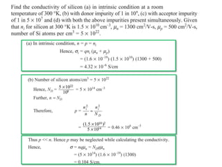
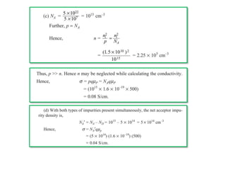
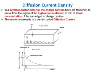
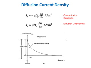
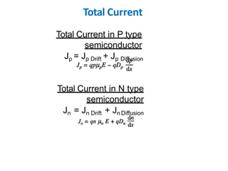
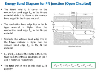
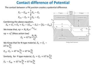
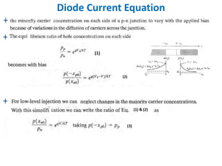
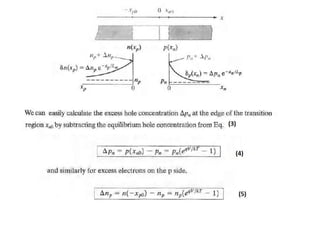
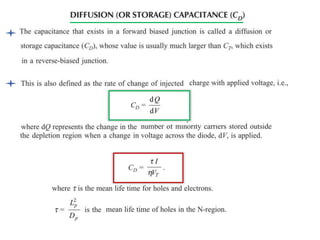
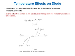
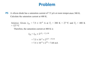
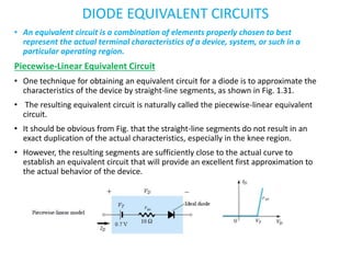
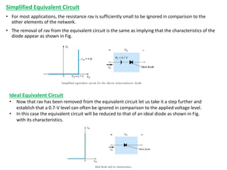
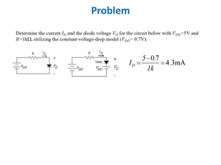
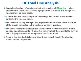
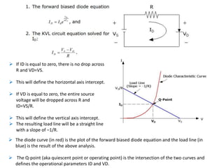
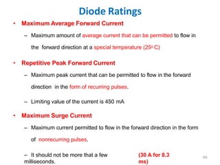
The document discusses semiconductor diodes and their operation. It covers:
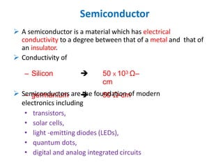
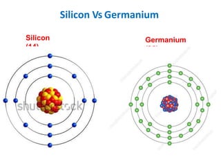
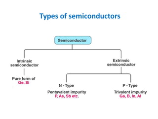
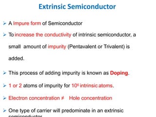
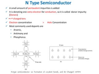
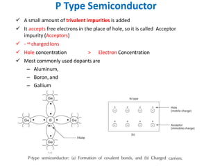
- Types of semiconductors including intrinsic and extrinsic semiconductors which are doped with impurities.
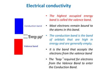
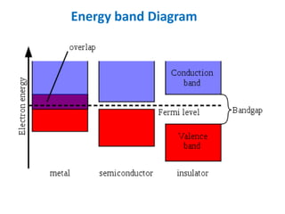
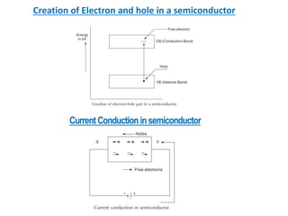
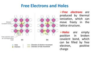
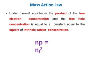
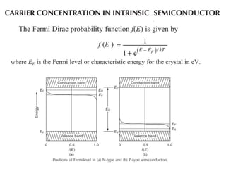
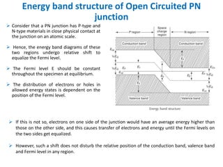
- The energy band structure of semiconductors including the valence band and conduction band. Carriers such as electrons and holes allow current flow.
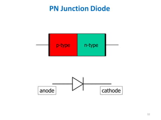
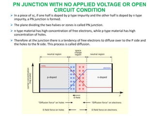
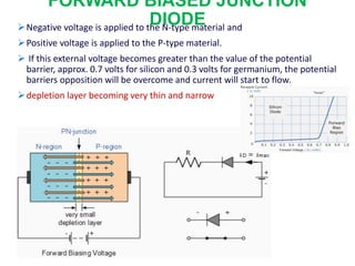
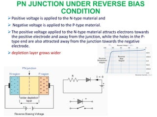
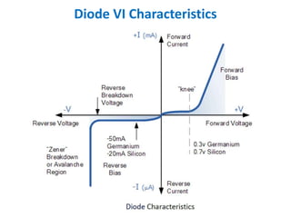
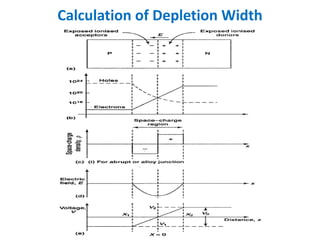
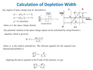
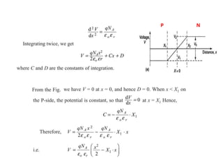
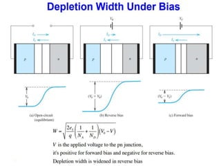
- PN junction diodes form when a P-type and N-type semiconductor are joined. Under forward bias the junction acts like a closed switch, under reverse bias it acts like an open switch.