Download as PDF, PPTX
![Microelectronics I
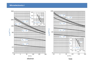
Conductivity
EEpneJ pndrf σµµ =+= )(
Drift current
σ; conductivity [( .cm)-1]
)( pne pn µµσ +=
electron
hole
Function of electron and hole concentrations and mobolities
Ρ; resistivity [ .cm]
)(
11
pne pn µµσ
ρ
+
==](https://image.slidesharecdn.com/chapter5carriertransportphenomena-161210152449/85/Chapter5-carrier-transport-phenomena-13-320.jpg)
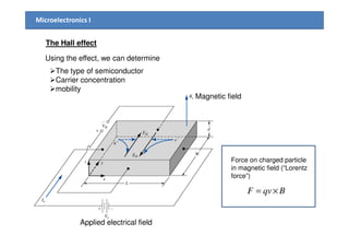

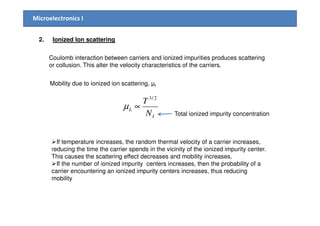
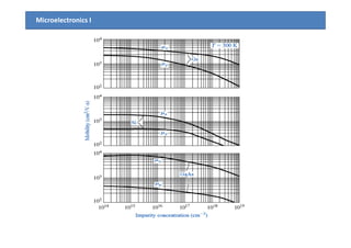
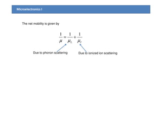
1) The document discusses carrier transport in semiconductors, including drift and diffusion currents. Carrier drift occurs due to an electric field and is characterized by carrier mobility, while diffusion is due to concentration gradients and characterized by the diffusion coefficient. 2) Mobility is affected by phonon and ionized impurity scattering. The net mobility is the sum of these scattering components. Conductivity is directly proportional to carrier concentration and mobility. 3) The Hall effect can be used to determine the type of semiconductor (n-type or p-type), carrier concentration, and carrier mobility. Measurement of the Hall voltage polarity indicates type, and its magnitude relates to concentration and mobility.


