This document provides an overview of semiconductors, diodes, transistors, and power devices. It discusses the energy band structure of semiconductors and classifications of intrinsic, n-type, and p-type semiconductors. The document then covers the theory and characteristics of PN junction diodes under forward and reverse bias conditions. Applications of diodes as rectifiers, clippers, and clampers are also discussed. Bipolar junction transistors and their biasing are introduced. Finally, the document discusses types of power converters including AC to DC converters using diode rectifiers and phase controlled rectifiers, as well as DC to DC converters.


![18
BIPOLAR JUNCTION TRANSISTOR [BJT]
A Bipolar Junction Transistor (BJT) is a three terminal
semiconductor device in which the operation depends on the
interaction of both majority and minority carriers and hence the
name Bipolar. It is used in amplifier and oscillator circuits, and as
a switch in digital circuits. It has wide applications in computers,
satellites and other modern communication systems.](https://image.slidesharecdn.com/beee-unit2-230315061609-d1477a3b/85/BEEE-pptx-18-320.jpg)


![53
SMPS-Switched Mode Power Supply [SMPS]
Various electrical and electronic loads are provided power using
batteries. But batteries do not provide regulated power as they offer
voltages of value either very high or very low. So, to obtain regulated dc
output, SMPS is used.
Unlike linear power supply, which uses the standard linear
method of voltage regulation, a switch mode power supply is a device that
performs voltage regulation of unregulated signal by using semiconductor
switching methods. It is considered to be highly efficient because it
lessens power consumption thereby showing a decrease in the amount of
heat dissipated. Thus, has replaced traditional linear power supply units.
SMPS includes a switching transistor (power MOSFET) for the
purpose of voltage regulation. During operation, the transistor switches
between on state and off state in a way that when it is on, it fully conducts
current with the negligible voltage drop across it. While when it is off, it
tries to completely block the flow of current. Thus, switching between on
state (saturated) and off state (cut-off) occurs at high frequency, and in
this way, the device acts as an ideal switch.
It is to be noted here that if the transformer operates at high
frequency, so the device size is reduced. Hence, the overall size of the
SMPS is small with less weight which is another advantage over linear
power supplies.](https://image.slidesharecdn.com/beee-unit2-230315061609-d1477a3b/85/BEEE-pptx-53-320.jpg)


![60
Realization [Implementation] of logic expression [Boolean Function ] using basic logic
gates](https://image.slidesharecdn.com/beee-unit2-230315061609-d1477a3b/85/BEEE-pptx-60-320.jpg)
![62
SUM OF PRODUCTS [SOP] AND PRODUCT OF SUMS
[POS]
Logical functions (Boolean expression) are generally
expressed in terms of logical variables (inputs) in
following forms. (Each input variable can have the
value, either 0 or 1 only)
•SUM OF PRODUCTS [SOP] Ex: AB’+ BC+C’D
•PRODUCT OF SUMS [POS] Ex: (A’+B’) (B’+C) (C’+D)
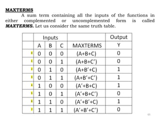
MINTERMS
A product term containing all the inputs of the
functions in either complemented or uncomplemented
form is called MINTERMS.
Let us consider 3 variable (input) function. It has
23 all possible combinations. [A ‘n’ variable (input)
function has 2n all possible combinations]. Let the
inputs are A, B, C and output is Y.](https://image.slidesharecdn.com/beee-unit2-230315061609-d1477a3b/85/BEEE-pptx-62-320.jpg)

![64
•In minterms, 0 are assigned with bar letter and
1 are assigned with unbar letter.
•Within the row, all are multiplied (Product)
•Choose only the output 1.
•Add the minterms which having 1 output.
•In this example, we get Y= A’BC’ + A’BC+ AB’C’+
ABC’. This expression is called canonical SOP
form. [Standard SOP form]
•Each input is assigned with it equivalent
decimal value. In the truth table, only the output
Y= 1 is chosen, it corresponding input’s decimal
values are stated as below.
Y= ∑m (2,3,4,6)](https://image.slidesharecdn.com/beee-unit2-230315061609-d1477a3b/85/BEEE-pptx-64-320.jpg)
![66
•In maxterms, 1 are assigned with bar letter and
0 are assigned with unbar letter.
•Within the row, all are summed (Added)
•Choose only the output 0.
•Product the maxterms which having 0 output.
•In this example, we get Y= (A+B+C) (A+B+C’)
(A’+B+C’) (A’+B’+C’). This expression is called
canonical POS form. [Standard POS form]
•Each input is assigned with it equivalent decimal
value. In the truth table, only the output Y= 0 is
chosen, it corresponding input’s decimal values
are stated as below.
Y= ∏M (0,1,5,7)
Note: Minterms and Maxterms are complement
with each other.](https://image.slidesharecdn.com/beee-unit2-230315061609-d1477a3b/85/BEEE-pptx-66-320.jpg)
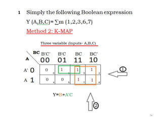
![67
1. For the Boolean function given below, obtain the (i)
canonical SOP form (ii) canonical POS form.
Y(A,B,C)= A+B’C
= AXX+ XB’C
= AB’C’+ AB’C+ ABC’+ ABC+A’B’C+ AB’C
[Remove the common term; Since A+A=A ]
Y= AB’C’+ AB’C+ ABC’+ ABC+A’B’C [Canonical
SOP form]
100 101 110 111 001
(m4 m5 m6 m7 m1)
Y= ∑m (1,4,5,6,7)
Y= ∏M (0,2,3) [ Minterms and Maxterms are
complement with each other]
M0 M2 M3
000 010 011
Y= (A+B+C) (A+B’+C) (A+B’+C’) [Canonical POS form]](https://image.slidesharecdn.com/beee-unit2-230315061609-d1477a3b/85/BEEE-pptx-67-320.jpg)


![71
4 (a) Solution Procedure for SOP method
(i) We have box ALL the 1.
(ii) Larger the box, smaller the equation. Since all are
minimization problem, we have chose larger box.
(iii) The number of 1’s inside the box must be 2n. [ie we have
to try boxing 16 , if not possible we have to try boxing 8, if not
possible we have to try boxing 4, if not possible we have to try
boxing 2, if not possible we have to box 1]
(iv) The shape of the box must
be square or rectangular. ie
(v) For each box, we have to find unchanged input.
For that, we have see K-map from right to left, then bottom to
top. The unchanged input within the box should be product.
The product of one box should be sum with next box.[In
input, 0 are assigned with bar letter and 1 are assigned with
unbar letter]
(vi) Overlapping is allowed to make larger box.](https://image.slidesharecdn.com/beee-unit2-230315061609-d1477a3b/85/BEEE-pptx-71-320.jpg)
![72
4 (b) Solution Procedure for POS method
(i) We have box ALL the 0.
(ii) Larger the box, smaller the equation. Since all are
minimization problem, we have chose larger box.
(iii) The number of 0’s inside the box must be 2n. [ie we have
to try boxing 16 , if not possible we have to try boxing 8, if not
possible we have to try boxing 4, if not possible we have to try
boxing 2, if not possible we have to box 1]
(iv) The shape of the box must
be square or rectangular. ie
(v) For each box, we have to find unchanged inputs.
For that, we have see K-map from right to left, then bottom to
top. The unchanged input within the box should be summed.
The sum of one box should be product with next box.[In
input, 1 are assigned with bar letter and 0 are assigned with
unbar letter]
(vi) Overlapping is allowed to make larger box.](https://image.slidesharecdn.com/beee-unit2-230315061609-d1477a3b/85/BEEE-pptx-72-320.jpg)


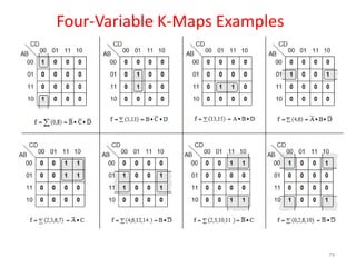


![83
3,4-Variable K-Maps Examples [POS]](https://image.slidesharecdn.com/beee-unit2-230315061609-d1477a3b/85/BEEE-pptx-83-320.jpg)