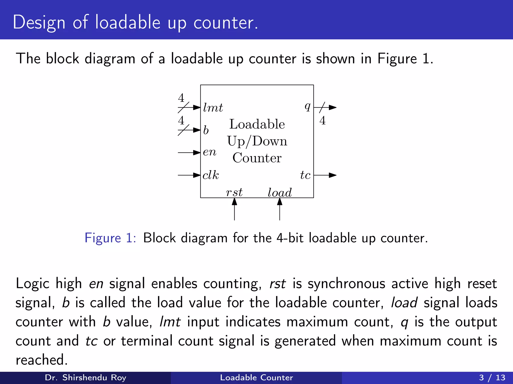
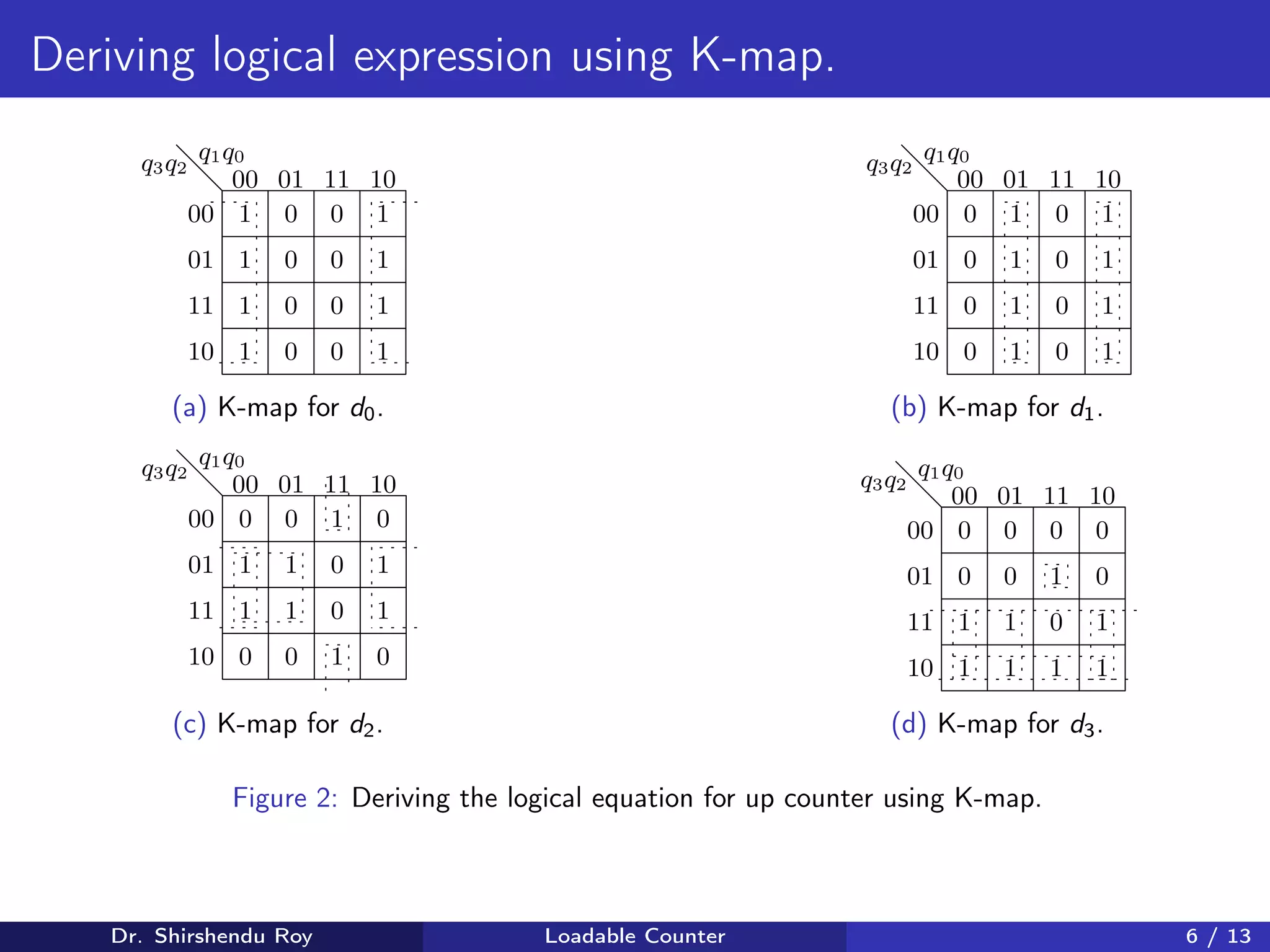
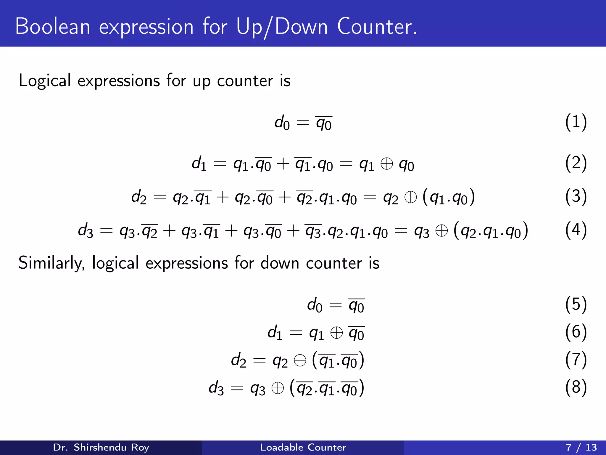
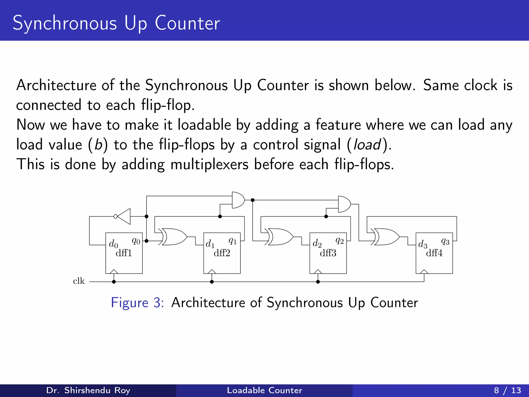
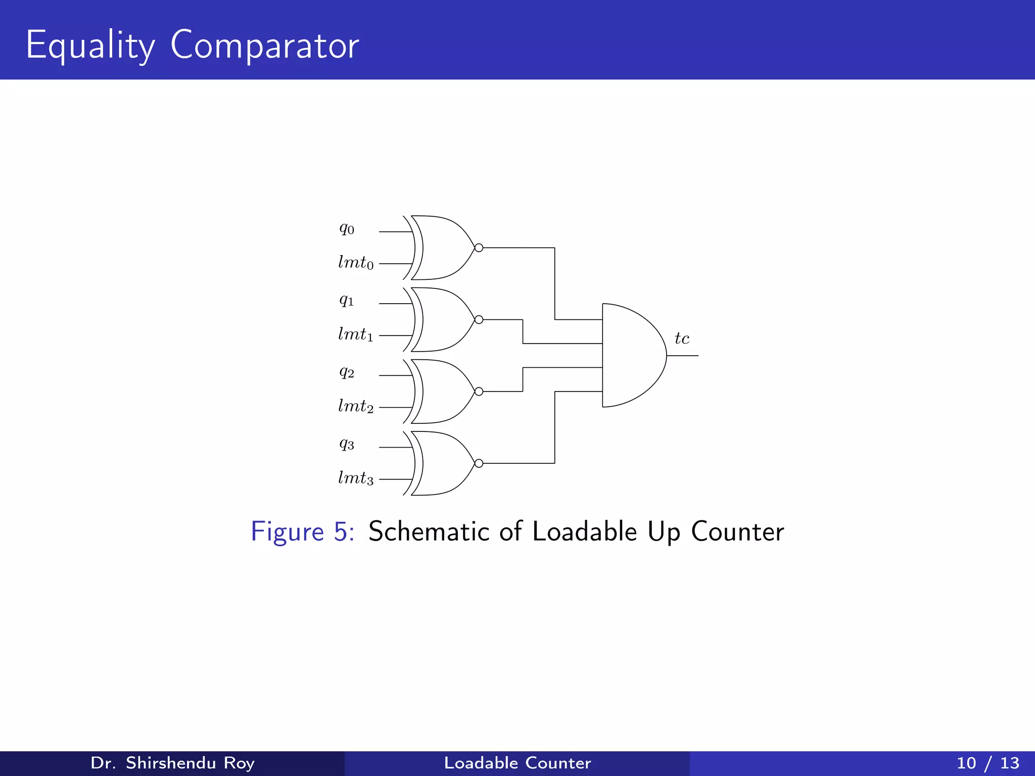
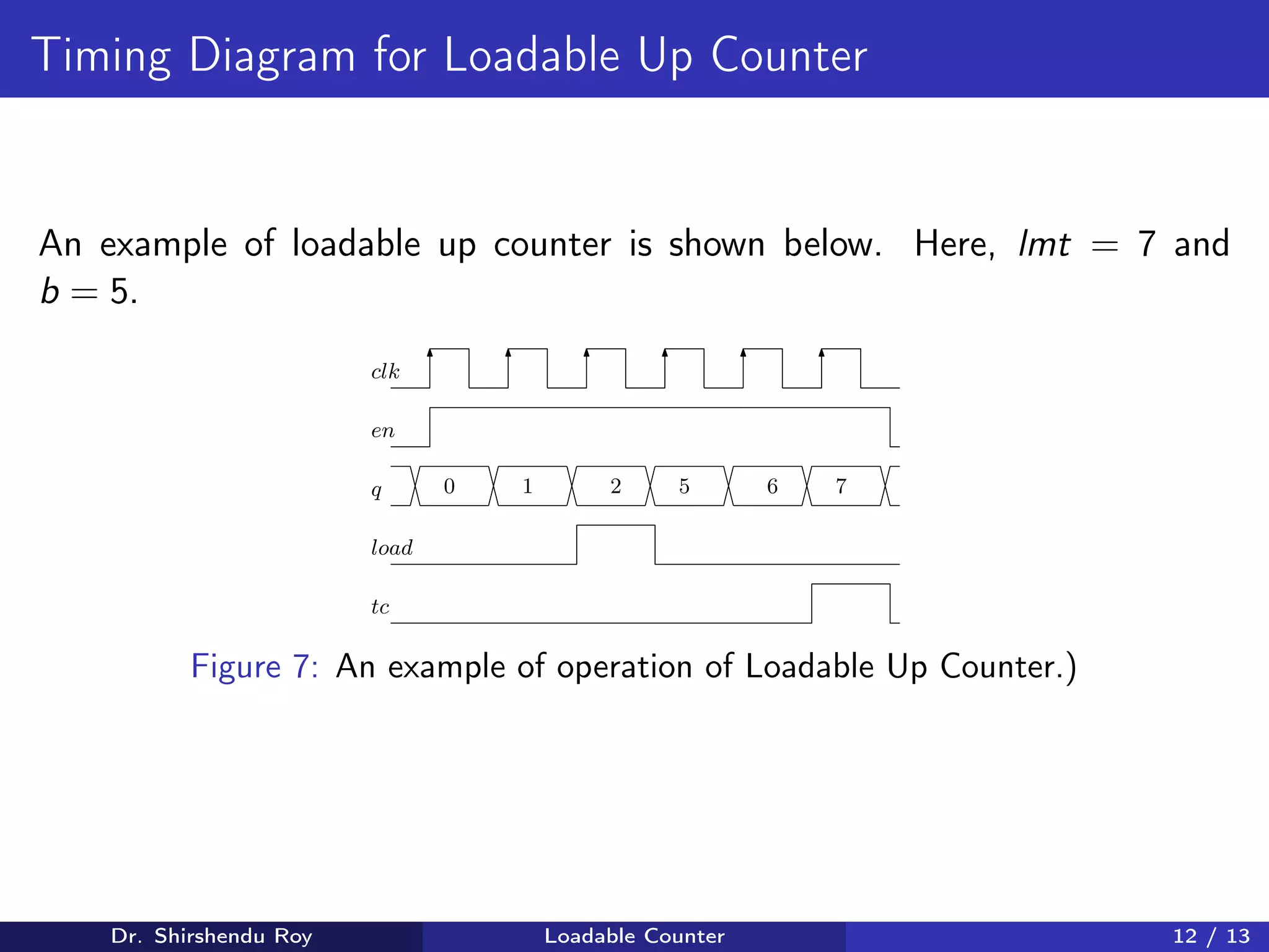
Design of Synchronous Loadable Up and Down Counter
Presented by
Dr. Shirshendu Roy
Homepage - https://digitalsystemdesign.in
Course - Digital Electronics
Dr. Shirshendu Roy Loadable Counter 1 / 13
Loadable up/down counter application
Loadable up or down counter is generalized synchronous counter which is
used
In any counting application (downward or upward).
In phase signal generation. These phase signals can be used to activate
or deactivate memory blocks.
In clock division circuits loadable counters can easily behave as MOD
counter.
In periodic or arbitrary counting loadable counters are used.
In starting a process or stopping any process.
Dr. Shirshendu Roy Loadable Counter 2 / 13
Design of loadable up counter.
The block diagram of a loadable up counter is shown in Figure 1.
Loadable
Up/Down
Counter
lmt
b
en
clk
rst load
tc
q
4
4 4
Figure 1: Block diagram for the 4-bit loadable up counter.
Logic high en signal enables counting, rst is synchronous active high reset
signal, b is called the load value for the loadable counter, load signal loads
counter with b value, lmt input indicates maximum count, q is the output
count and tc or terminal count signal is generated when maximum count is
reached.
Dr. Shirshendu Roy Loadable Counter 3 / 13
Design Procedure
Design procedure steps for loadable counter are
In order to design a loadable up counter, first step is to know how to
design synchronous up counter from its truth table.
Selection of flip/flop by which the counter will be designed.
Here, 4-bit counter will be designed and D flip-flop is chosen for realizing
the counter.
Thus four flip-flops will be required. Here, q3q2q1q0 denotes present
states (PS) of the flip-flops and q∗
3q∗
2q∗
1q∗
0 are next states (NS).
We have find the expression for the inputs of the flip-flops (d3, d2, d1
and d0).
In case D flip-flop, input of the flip-flops follows the status of the next
states.
K-map is used here to find the expression for inputs.
.
Dr. Shirshendu Roy Loadable Counter 4 / 13
Truth table for synchronous up counter.
Table 1: Truth table for synchronous up counter.
Decimal q3q2q1q0 q∗
3q∗
2q∗
1q∗
0 d3 d2 d1 d0
0 0000 0001 0 0 0 1
1 0001 0010 0 0 1 0
2 0010 0011 0 0 1 1
3 0011 0100 0 1 0 0
4 0100 0101 0 1 0 1
5 0101 0110 0 1 1 0
6 0110 0111 0 1 1 1
7 0111 1000 1 0 0 0
8 1000 1001 1 0 0 1
9 1001 1010 1 0 1 0
10 1010 1011 1 0 1 1
11 1011 1100 1 1 0 0
12 1100 1101 1 1 0 1
13 1101 1110 1 1 1 0
14 1110 1111 1 1 1 1
15 1111 0000 0 0 0 0
Dr. Shirshendu Roy Loadable Counter 5 / 13
Deriving logical expression using K-map.
q3q2
q1q0
00 01 11 10
00
01
11
10
1
1
1
1
1
1
1
1
0 0
0 0
0 0
0 0
(a) K-map for d0.
q3q2
q1q0
00 01 11 10
00
01
11
10
1
1
1
1
0
0
0
0
0
0
0
0
1
1
1
1
(b) K-map for d1.
q3q2
q1q0
00 01 11 10
00
01
11
10
1
0
0
1
0
1
1
1
1
0
0
0
0
0
1
1
(c) K-map for d2.
q3q2
q1q0
00 01 11 10
00
01
11
10
0
1
0
1
0 0
1
0
0
1
1
1
1
1
0
0
(d) K-map for d3.
Figure 2: Deriving the logical equation for up counter using K-map.
Dr. Shirshendu Roy Loadable Counter 6 / 13
Boolean expression for Up/Down Counter.
Logical expressions for up counter is
d0 = q0 (1)
d1 = q1.q0 + q1.q0 = q1 ⊕ q0 (2)
d2 = q2.q1 + q2.q0 + q2.q1.q0 = q2 ⊕ (q1.q0) (3)
d3 = q3.q2 + q3.q1 + q3.q0 + q3.q2.q1.q0 = q3 ⊕ (q2.q1.q0) (4)
Similarly, logical expressions for down counter is
d0 = q0 (5)
d1 = q1 ⊕ q0 (6)
d2 = q2 ⊕ (q1.q0) (7)
d3 = q3 ⊕ (q2.q1.q0) (8)
Dr. Shirshendu Roy Loadable Counter 7 / 13
Synchronous Up Counter
Architecture of the Synchronous Up Counter is shown below. Same clock is
connected to each flip-flop.
Now we have to make it loadable by adding a feature where we can load any
load value (b) to the flip-flops by a control signal (load).
This is done by adding multiplexers before each flip-flops.
d0
dff1 dff2 dff3 dff4
q0 d1
q1 d2
q2 d3
q3
clk
Figure 3: Architecture of Synchronous Up Counter
Dr. Shirshendu Roy Loadable Counter 8 / 13
Schematic of Loadable Up Counter
0
1
d0
0
1
0
1
0
1
dff1 dff2 dff3 dff4
q0 d1
q1 d2
q2 d3
q3
b0 b1 b2 b3
clk
reset
load
en
Equality
Comparator
q[3 : 0]
lmt[3 : 0]
tc
Figure 4: Schematic of Loadable Up Counter
Whenever the load signal is high input b is passed to the flip-flops and
whenever the counter reaches lmt value a tc signal is generated by a equality
comparator.
Dr. Shirshendu Roy Loadable Counter 9 / 13
Equality Comparator
q0
lmt0
q1
lmt1
q2
lmt2
q3
lmt3
tc
Figure 5: Schematic of Loadable Up Counter
Dr. Shirshendu Roy Loadable Counter 10 / 13
Schematic of Loadable Down Counter
Similarly, we can design a loadable down counter.
0
1
d0
0
1
0
1
0
1
dff1 dff2 dff3 dff4
q0 d1
q1 d2
q2 d3
q3
b0 b1 b2 b3
clk
reset
load
en
Figure 6: Architecture of Loadable Down Counter.
Dr. Shirshendu Roy Loadable Counter 11 / 13
Timing Diagram for Loadable Up Counter
An example of loadable up counter is shown below. Here, lmt = 7 and
b = 5.
clk
en
q 0 1 2 5 6 7
load
tc
Figure 7: An example of operation of Loadable Up Counter.)
Dr. Shirshendu Roy Loadable Counter 12 / 13
Thank You
Dr. Shirshendu Roy Loadable Counter 13 / 13

Synchronous Loadable Up and Down Counter

  • 1.
    Design of SynchronousLoadable Up and Down Counter Presented by Dr. Shirshendu Roy Homepage - https://digitalsystemdesign.in Course - Digital Electronics Dr. Shirshendu Roy Loadable Counter 1 / 13
  • 2.
    Loadable up/down counterapplication Loadable up or down counter is generalized synchronous counter which is used In any counting application (downward or upward). In phase signal generation. These phase signals can be used to activate or deactivate memory blocks. In clock division circuits loadable counters can easily behave as MOD counter. In periodic or arbitrary counting loadable counters are used. In starting a process or stopping any process. Dr. Shirshendu Roy Loadable Counter 2 / 13
  • 3.
    Design of loadableup counter. The block diagram of a loadable up counter is shown in Figure 1. Loadable Up/Down Counter lmt b en clk rst load tc q 4 4 4 Figure 1: Block diagram for the 4-bit loadable up counter. Logic high en signal enables counting, rst is synchronous active high reset signal, b is called the load value for the loadable counter, load signal loads counter with b value, lmt input indicates maximum count, q is the output count and tc or terminal count signal is generated when maximum count is reached. Dr. Shirshendu Roy Loadable Counter 3 / 13
  • 4.
    Design Procedure Design proceduresteps for loadable counter are In order to design a loadable up counter, first step is to know how to design synchronous up counter from its truth table. Selection of flip/flop by which the counter will be designed. Here, 4-bit counter will be designed and D flip-flop is chosen for realizing the counter. Thus four flip-flops will be required. Here, q3q2q1q0 denotes present states (PS) of the flip-flops and q∗ 3q∗ 2q∗ 1q∗ 0 are next states (NS). We have find the expression for the inputs of the flip-flops (d3, d2, d1 and d0). In case D flip-flop, input of the flip-flops follows the status of the next states. K-map is used here to find the expression for inputs. . Dr. Shirshendu Roy Loadable Counter 4 / 13
  • 5.
    Truth table forsynchronous up counter. Table 1: Truth table for synchronous up counter. Decimal q3q2q1q0 q∗ 3q∗ 2q∗ 1q∗ 0 d3 d2 d1 d0 0 0000 0001 0 0 0 1 1 0001 0010 0 0 1 0 2 0010 0011 0 0 1 1 3 0011 0100 0 1 0 0 4 0100 0101 0 1 0 1 5 0101 0110 0 1 1 0 6 0110 0111 0 1 1 1 7 0111 1000 1 0 0 0 8 1000 1001 1 0 0 1 9 1001 1010 1 0 1 0 10 1010 1011 1 0 1 1 11 1011 1100 1 1 0 0 12 1100 1101 1 1 0 1 13 1101 1110 1 1 1 0 14 1110 1111 1 1 1 1 15 1111 0000 0 0 0 0 Dr. Shirshendu Roy Loadable Counter 5 / 13
  • 6.
    Deriving logical expressionusing K-map. q3q2 q1q0 00 01 11 10 00 01 11 10 1 1 1 1 1 1 1 1 0 0 0 0 0 0 0 0 (a) K-map for d0. q3q2 q1q0 00 01 11 10 00 01 11 10 1 1 1 1 0 0 0 0 0 0 0 0 1 1 1 1 (b) K-map for d1. q3q2 q1q0 00 01 11 10 00 01 11 10 1 0 0 1 0 1 1 1 1 0 0 0 0 0 1 1 (c) K-map for d2. q3q2 q1q0 00 01 11 10 00 01 11 10 0 1 0 1 0 0 1 0 0 1 1 1 1 1 0 0 (d) K-map for d3. Figure 2: Deriving the logical equation for up counter using K-map. Dr. Shirshendu Roy Loadable Counter 6 / 13
  • 7.
    Boolean expression forUp/Down Counter. Logical expressions for up counter is d0 = q0 (1) d1 = q1.q0 + q1.q0 = q1 ⊕ q0 (2) d2 = q2.q1 + q2.q0 + q2.q1.q0 = q2 ⊕ (q1.q0) (3) d3 = q3.q2 + q3.q1 + q3.q0 + q3.q2.q1.q0 = q3 ⊕ (q2.q1.q0) (4) Similarly, logical expressions for down counter is d0 = q0 (5) d1 = q1 ⊕ q0 (6) d2 = q2 ⊕ (q1.q0) (7) d3 = q3 ⊕ (q2.q1.q0) (8) Dr. Shirshendu Roy Loadable Counter 7 / 13
  • 8.
    Synchronous Up Counter Architectureof the Synchronous Up Counter is shown below. Same clock is connected to each flip-flop. Now we have to make it loadable by adding a feature where we can load any load value (b) to the flip-flops by a control signal (load). This is done by adding multiplexers before each flip-flops. d0 dff1 dff2 dff3 dff4 q0 d1 q1 d2 q2 d3 q3 clk Figure 3: Architecture of Synchronous Up Counter Dr. Shirshendu Roy Loadable Counter 8 / 13
  • 9.
    Schematic of LoadableUp Counter 0 1 d0 0 1 0 1 0 1 dff1 dff2 dff3 dff4 q0 d1 q1 d2 q2 d3 q3 b0 b1 b2 b3 clk reset load en Equality Comparator q[3 : 0] lmt[3 : 0] tc Figure 4: Schematic of Loadable Up Counter Whenever the load signal is high input b is passed to the flip-flops and whenever the counter reaches lmt value a tc signal is generated by a equality comparator. Dr. Shirshendu Roy Loadable Counter 9 / 13
  • 10.
    Equality Comparator q0 lmt0 q1 lmt1 q2 lmt2 q3 lmt3 tc Figure 5:Schematic of Loadable Up Counter Dr. Shirshendu Roy Loadable Counter 10 / 13
  • 11.
    Schematic of LoadableDown Counter Similarly, we can design a loadable down counter. 0 1 d0 0 1 0 1 0 1 dff1 dff2 dff3 dff4 q0 d1 q1 d2 q2 d3 q3 b0 b1 b2 b3 clk reset load en Figure 6: Architecture of Loadable Down Counter. Dr. Shirshendu Roy Loadable Counter 11 / 13
  • 12.
    Timing Diagram forLoadable Up Counter An example of loadable up counter is shown below. Here, lmt = 7 and b = 5. clk en q 0 1 2 5 6 7 load tc Figure 7: An example of operation of Loadable Up Counter.) Dr. Shirshendu Roy Loadable Counter 12 / 13
  • 13.
    Thank You Dr. ShirshenduRoy Loadable Counter 13 / 13