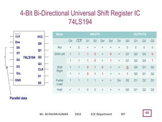
Downloaded 46 times

![58
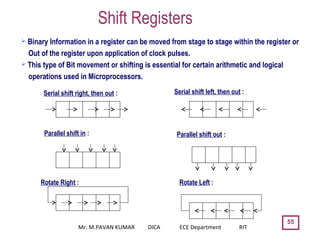
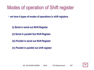
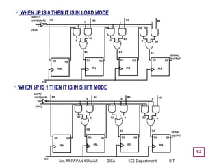
When we transfer data in SISO manner then we taken output at last flipfliop. i.e.
Q0 and input as first flipflop i.e Q2.
Time consumed for clock to store N bits is = [ N+N-1] * T
= [ 2N-1]*T , N= no.of Bits, T= clock duration
Suppose we have 2msec duration for one cycle. Then for 4-bit it will have
= [2(4)-1]*2
= 14msec.
Note: for GATE
Mr. M.PAVAN KUMAR DICA ECE Department RIT](https://image.slidesharecdn.com/sequntiallogicdesign-180926100126/85/Sequntial-logic-design-58-320.jpg)
![60
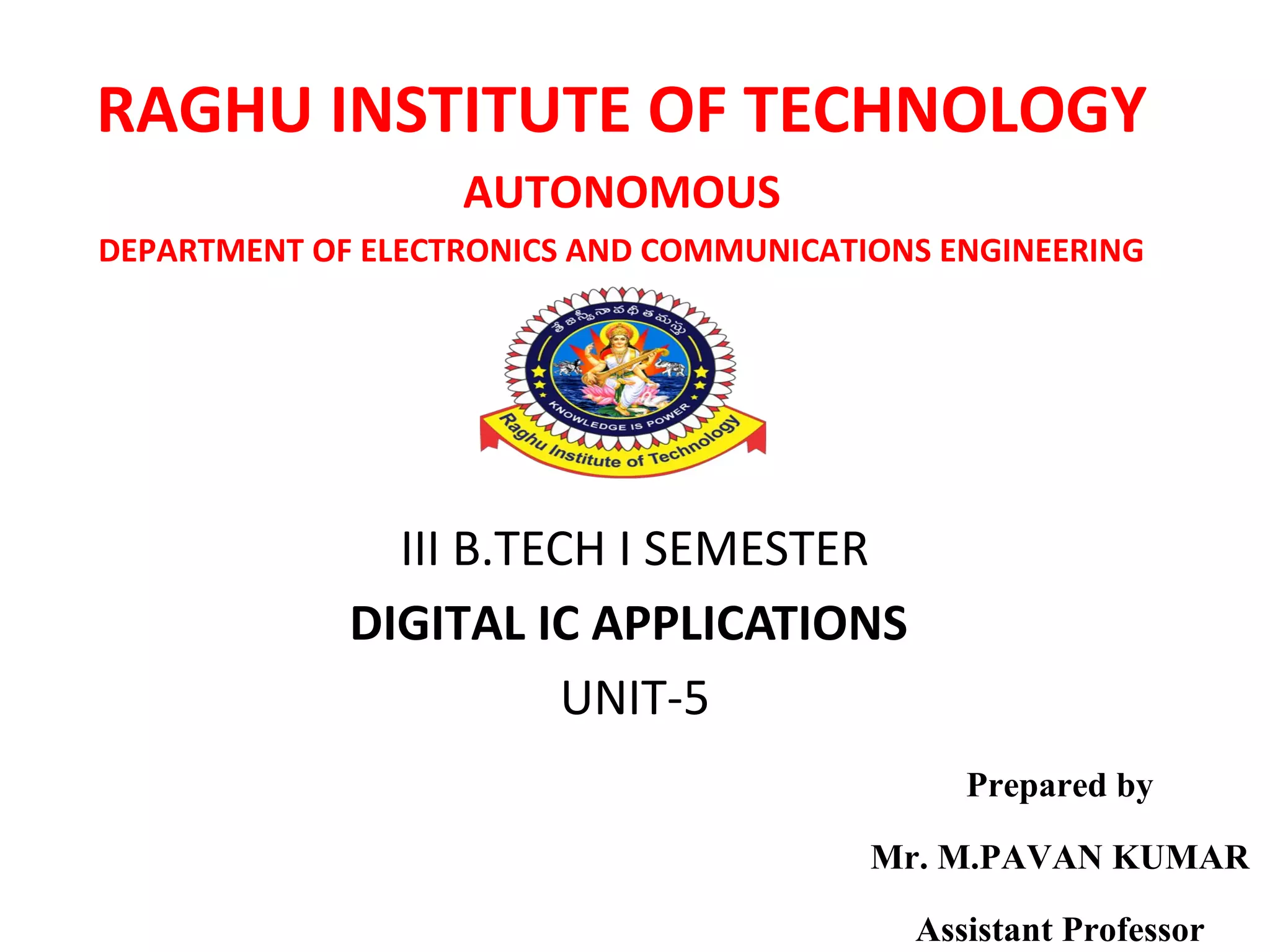
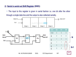
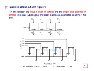
When we transfer data in SIPO manner then we taken output at each and every
flipfliop. i.e. Q0,Q1,Q2
Time consumed for clock to store N bits is = [ N ] * T
N= no.of Bits, T= clock duration
Suppose we have 2msec duration for one cycle. Then for 4-bit it will have
= (4)*2 = 8msec.
Note: for GATE
Total time consumed by the clock to store the bits in SISO manner = [2N-1]*T
Total time consumed by the clock to store the bits in SIPO manner= N*T
Mr. M.PAVAN KUMAR DICA ECE Department RIT](https://image.slidesharecdn.com/sequntiallogicdesign-180926100126/85/Sequntial-logic-design-60-320.jpg)

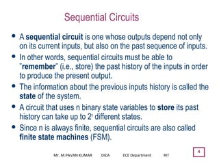
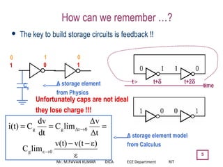
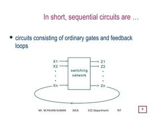
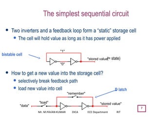
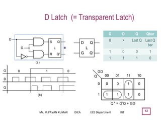
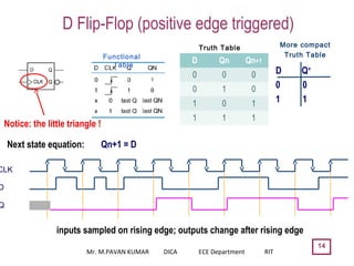
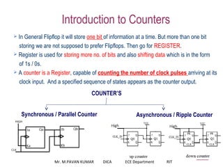
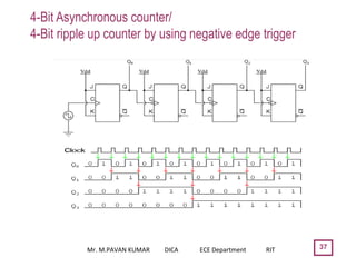
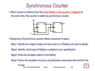
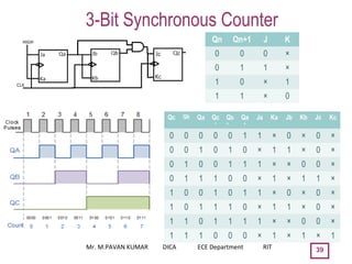
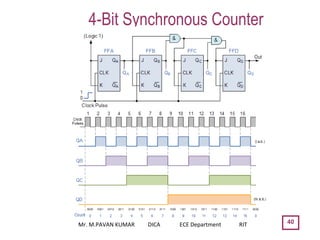
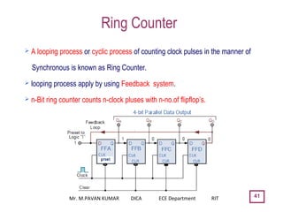
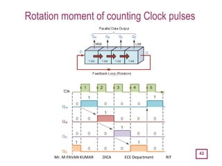
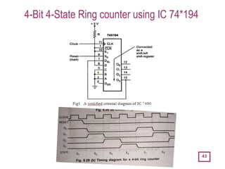
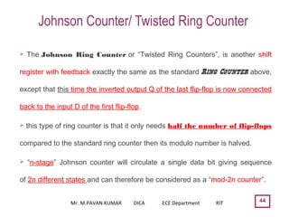
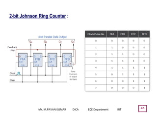
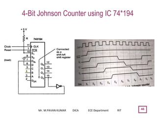
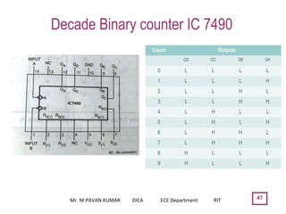
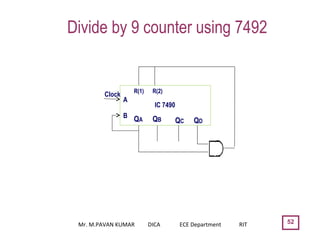
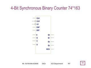
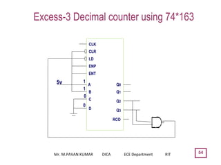
This document discusses sequential digital circuits and various counter circuits. It begins with an introduction to sequential circuits and how they differ from combinational circuits in their ability to store state. Common storage elements like latches and flip-flops are described along with their characteristics. Various types of latches and flip-flops such as D, JK, and T flip-flops are defined. The document then covers counter circuits like synchronous and asynchronous counters. Specific counter circuits like ring counters and Johnson counters are explained. Implementation of 4-bit synchronous and asynchronous counters using flip-flops is demonstrated. Finally, a decade counter integrated circuit is briefly described.