ERODE SENGUNTHAR ENGINEERINGCOLLEGE
(Autonomous)
Approved by AICTE, New Delhi, Permanently Affiliated to Anna University- Chennai,
Accredited by National Board of Accreditation (NBA), New Delhi &
National Assessment and Accreditation Council (NAAC), Bangalore with ‘A’ Grade
PERUNDURAI, ERODE – 638 057.
DEPARTMENT OF
ELECTRONICS AND COMMUNICATION
ENGINEERING
ACADEMIC YEAR (2024-2025)
19EC704 Optical and Microwave
Laboratory
Prepared By
Dr.V.THAMIZHARASAN, AP/ECE
2.
ERODE SENGUNTHAR ENGINEERINGCOLLEGE
(Autonomous)
Approved by AICTE, New Delhi, Permanently Affiliated to Anna University- Chennai,
Accredited by National Board of Accreditation (NBA), New Delhi &
National Assessment and Accreditation Council (NAAC), Bangalore with ‘A’ Grade
PERUNDURAI, ERODE – 638 057.
DEPARTMENT OF ELECTRONICS AND COMMUNICATION ENGINEERING
VISION
To become a full fledged department by preparing the engineers/ students to meet the needs of
latest technological advancements in Electronics and Communication Engineering field and
offering quality education through innovative and ethical aspects , which focus on societal
empowerment.
MISSION
The Vision of the Department will be achieved by,
M1: To Provide best and unique learning environment for the students to
compete with global standards.
M2: Establishing Center of Excellence in latest domain to foster the creativity
among faculty and students
M3: To provide lifelong learning through ethical and value based education and
making the students entrepreneur and employable
3.
Department of Electronicsand Communication
Engineering
Program Outcomes (PO)
1. Engineering knowledge: Apply the knowledge of mathematics, science, engineering
fundamentals, and an engineering specialization to the solution of complex engineering
problems.
2. Problem analysis: Identify, formulate, review research literature, and analyze complex
engineering problems reaching substantiated conclusions using first principles of mathematics,
natural sciences, and engineering sciences.
3. Design/development of solutions: Design solutions for complex engineering problems and
design system components or processes that meet the specified needs with appropriate
consideration for the public health and safety, and the cultural, societal, and environmental
considerations.
4. Conduct investigations of complex problems: Use research-based knowledge and research
methods including design of experiments, analysis and interpretation of data, and synthesis of the
information to provide valid conclusions.
5. Modern tool usage: Create, select, and apply appropriate techniques, resources, and modern
engineering and IT tools including prediction and modeling to complex engineering activities
with an understanding of the limitations.
6. The engineer and society: Apply reasoning informed by the contextual knowledge to assess
societal, health, safety, legal and cultural issues and the consequent responsibilities relevant to
the professional engineering practice.
7. Environment and sustainability: Understand the impact of the professional engineering
solutions in societal and environmental contexts, and demonstrate the knowledge of, and need
for sustainable development.
8. Ethics: Apply ethical principles and commit to professional ethics and responsibilities and norms
of the engineering practice.
9. Individual and team work: Function effectively as an individual, and as a member or leader in
diverse teams, and in multidisciplinary settings.
4.
10. Communication: Communicateeffectively on complex engineering activities with the
engineering community and with society at large, such as, being able to comprehend and write
effective reports and design documentation, make effective presentations, and give and receive
clear instructions.
11. Project management and finance: Demonstrate knowledge and understanding of the
engineering and management principles and apply these to one’s own work, as a member and
leader in a team, to manage projects and in multidisciplinary environments.
12. Life-long learning: Recognize the need for, and have the preparation and ability to engage in
independent and life-long learning in the broadest context of technological change.
PROGRAM SPECIFIC OUTCOMES (PSO)
PSO1 : Interpretation Skills: Acquire skills to design, verify and validate electronic functional
elements for a variety of applications
PS02: Core Competences: Ability to use hardware and software tools to solve complex
problems in VLSI, Communication, RF and Embedded Systems.
PS03: Attitude: Aware of social and environmental issues with ethical responsibility to
implement any useful, frugal and eco-friendly systems for the society.
PROGRAMME EDUCATIONAL OBJECTIVES (PEOS)
Impart the learners, an ability to understand and use analytical, academic and communication skills
effectively with special emphasis to fulfill societal needs. (Comprehend)
Inspire the beginners to enrich their skills throughout career by learning about emerging
technologies, adapting and accepting the changes to achieve leadership position in industry or
academia. (Enthusiasm for learning)
Graduate electronic engineers capable of employing necessary hardware / software tools and
interdisciplinary skills for modern engineering applications, thereby to boost the economy of the
region and the nation. (Proficient Employment)
Prepare Graduates to work effectively on team based engineering venture and practice ethics of
their profession consistent with a sense of social responsibility. (Professional Ethics)
5.
Department ELECTRONICS ANDCOMMUNICATION ENGINEERING R 2019 Semester-VII PC
Course Code Course Name Hours / Week Credit Total
Hours
Maximum Marks
19EC704
OPTICAL AND MICROWAVE
LABORATORY
L T P C
0 0 3 1 45 100
Course Objective (s): The purpose of learning this course is to
Study the characteristic of passive microwave components
Learn the radiation characteristics of microwave antennas
Study the characteristics of Microwave sources
Perform experiment to verify the characteristics of optical source
Analyze the performance of fiber optic communication link
Course Outcomes: At the end of this course, learners will be able to:
Measure and analyze the parameters of rectangular waveguides
Conduct experiments to measure the characteristics of passive microwave components
Measure and analyze the radiation characteristics of microwave antennas
Verify the characteristics of Microwave sources
Measure and verify the characteristics of optical source
Exp
No.
Microwave Experiments
1 Reflex Klystron mode characteristics
2 Radiation pattern of Horn antenna
3 Impedance measurement using VSWR
4 Power measurement of Gunn Diode oscillator
5 Characteristics of Gunn Diode oscillator
6 Determination of coupling factor, insertion loss, isolation and directivity of directional coupler
Exp No. Optical Experiments
1
1
Measurement of Bending loss
2 Measurement of the numerical aperture and data communication system using a fibre-optic
system
3 LED/Laser diode characteristics
4 Mode characteristics of an optical fiber & digital link establishment using LED/Laser diode
Content beyond the syllabus:
Measurement of propagation losses using a fibre-optic system(Content Beyond Syllabus)
Learning Resources
Books:
1. Gerd Keiser, "Optical Fiber Communication" Mc Graw -Hill International, 4th Edition. 2010.
2. John M. Senior , “Optical Fiber Communication”, Second Edition, Pearson Education, 2007.
3. Robert E Colin, “Foundations for Microwave Engineering”, John Wiley & Sons Inc, 2005
Web Resources :
www.cisco.com/c/en/us/products/optical-networking
www.hit.bme.hu/~jakab/edu/litr/wdm/opt_net.pdf.
networks.nokia.com/in/portfolio/products/optical-networking
List of Experiments:
6.
1. Mode characteristicsof Reflex Klystron
2. Characteristics of Gunn Diode oscillator
3. Measurement of numerical aperture
4. Measurement of propagation losses, Bending loss using a fibre-optic system (Content
Beyond Syllabus)
5. Impedance measurement using VSWR
6. Radiation pattern of Horn antenna
7. Determination of coupling factor, insertion loss, isolation and directivity of directional
coupler
8. LED/Laser diode characteristics
9. Mode characteristics of an optical fiber & digital link establishment using LED/Laser diode
10. Data Communication using Optical fiber
11. Power measurement of Gunn Diode oscillator
STUDY OF MICROWAVE COMPONENTS
7.
AIM
To study themicrowave components in the laboratory.
COMPONENTS
Isolator
Variable attenuator
Frequency meter
Short termination
Matched termination
Directional Coupler
Horn antenna
Magic tee
Circulator
Detector mount
THEORY:
ISOLATOR
An isolator is a two-port device that transmits microwave or radio frequency power in
one direction only. It is used to shield equipment on its input side, from the effects of conditions
on its output side; for example, to prevent a microwave source being detuned by a mismatched
load. To achieve non-reciprocity, an isolator must necessarily incorporate a non-reciprocal
material. At microwave frequencies this material is invariably a ferrite which is biased by a static
magnetic field. The ferrite is positioned within the isolator such that the microwave signal
presents it with a rotating magnetic field, with the rotation axis aligned with the direction of the
static bias field.
The behaviour of the ferrite depends on the sense of rotation with respect to the bias field, and
hence is different for microwave signals travelling in opposite directions. Depending on the exact
operating conditions, the signal travelling in one direction may either be phase-shifted, displaced
from the ferrite or absorbed.
VARIABLE ATTENUATOR
8.
An attenuator isan electronic device that reduces the amplitude or power of a signal
without appreciably distorting its waveform. An attenuator is effectively the opposite of an
amplifier, though the two work by different methods. While an amplifier provides gain, an
attenuator provides loss, or gain less than 1.
Attenuators are usually passive devices made from simple voltage divider networks. Switching
between different resistances forms adjustable stepped attenuators and continuously adjustable
ones using potentiometers. For higher frequencies precisely matched low VSWR resistance
networks are used.
Fixed attenuators in circuits are used to lower voltage, dissipate power, and to improve
impedance matching. In measuring signals, attenuator pads or adaptors are used to lower the
amplitude of the signal a known amount to enable measurements, or to protect the measuring
device from signal levels that might damage it. Attenuators are also used to 'match' impedances
by lowering apparent SWR.
FIXED ATTENUATORS
With the help of our experienced engineers, we are able to design and develop a wide and
comprehensive range of Fixed Attenuators, which is available at market leading prices. This
range of fixed attenuators is highly acclaimed in the industry, owing to its application in
networks, telecommunication, instruments and allied fronts. The offered range of fixed
attenuators is applauded for its below cited features:
High attenuation precision
Excellent stability
Excellent reliability.
MOVABLE SHORTS:
We are highly appreciated in the domestic and international market for an unparalleled
range of Movable Shorts. These products are utilized in different experiments such as to
study the characteristics of reflex klystron and frequency, guide wavelength and free
space wave length. In addition to this, the offered range is skillfully developed by our
diligent engineers, who possess commendable experience, in-depth knowledge and
expertise in this domain.
PRECISION MOVABLE SHORTS:
9.
Our organization iscounted amongst the most distinguished manufacturers and
traders of a wide range of Precision Movable Shorts. The offered range of precision movable
shorts is available in different forms, sizes, grades and models as per the emerging requirements
of the honorable patrons. Besides, these products are highly appreciated for their compact design,
sturdy construction and durable finish standards. Customers can avail these products at market
leading prices.
FREQUENCY METER
The frequency meter is classified into two categories namely direct and indirect
frequency meter. Moving a plunger can vary the distance between the shorted tuning and diode.
The timing arrangement helps the user to read just the distance from the short circuit wherever
the signal frequency. The detector output is normally available in at the coaxial connector, the
crystal diode act as a square law device. The response of the diode to the power is dependent on
resistance of the mount the diode used for detection in X band is IN238.
DIRECT READOUT FREQUENCY METER
The frequency meter is classified into two categories namely direct and indirect
frequency meter. Moving a plunger can vary the distance between the shorted tuning and diode.
The timing arrangement helps the user to read just the distance from the short circuit wherever
the signal frequency. The detector output is normally available in at the coaxial connector, the
crystal diode act as a square law device. The response of the diode to the power is dependent on
resistance of the mount the diode used for detection in X band is IN238.
SHORT TERMINATION
This is termination of load for a microwave setup. In short termination the current is
maximum whereas the voltage is zero. The standing wave thus has a maximum or minimum at a
short end.
MATCHED TERMINATION
10.
This is alsoa termination of load for microwave setup, standing wave occurs when a
load does not completely absorb the power reaching it. Microwave measurement requires a
termination resulting in maximum reflection, when matched terminations serve the purpose.
DIRECTIONAL COUPLER
Power dividers (also power splitters and, when used in reverse, power combiners)
and directional couplers are passive devices used in the field of radio technology. They couple a
defined amount of the electromagnetic power in a transmission line to another port where it can
be used in another circuit. An essential feature of directional couplers is that they only couple
power flowing in one direction. Power entering the output port is not coupled.
Directional couplers are most frequently constructed from two coupled transmission lines set
close enough together such that energy passing through one is coupled to the other. This
technique is favoured due to the microwave frequencies the devices are commonly employed
with. However, lumped component devices are also possible at lower frequencies.
Directional couplers and power dividers have many applications, these include; providing a
signal sample for measurement or monitoring, feedback, combining feeds to and from antennae,
and providing taps for cable distributed systems such as cable TV.
MULTI HOLE DIRECTIONAL COUPLER 3DB
Backed by rich industry experience, we are presenting an unparalleled range of Multi
Hole Directional Coupler 3DB. The offered range of multi hole directional coupler 3 db is best
suited for power control and demodulation. These products are manufactured utilizing the
sophisticated microwave CAD software and advanced machinery, in strict compliance with the
set industry norms and guidelines.
Features:
Sturdy construction
Durable
High performance
Elegant finish.
HORN ANTENNA
11.
A horn antennaor microwave horn is an antenna that consists of a flaring metal
waveguide shaped like a horn to direct the radio waves. Horns are widely used as antennas at
UHF and microwave frequencies, above 300 MHz. They are used as feeders (called feed horns)
for larger antenna structures such as parabolic antennas, as standard calibration antennas to
measure the gain of other antennas, and as directive antennas for such devices as radar guns,
automatic door openers, and microwave radiometers. Their advantages are moderate directivity
(gain), low SWR, broad bandwidth, and simple construction and adjustment.
An advantage of horn antennas is that since they don't have any resonant elements, they can
operate over a wide range of frequencies, a wide bandwidth. The useable bandwidth of horn
antennas is typically of the order of 10:1, and can be up to 20:1 (for example allowing it to
operate from 1 GHz to 20 GHz). The input impedance is slowly-varying over this wide
frequency range, allowing low VSWR over the bandwidth.The gain of horn antennas ranges up
to 25 dBi, with 10 - 20 dBi being typical.
MAGIC TEE
A magic tee (or magic T or hybrid tee) is a hybrid or 3dB coupler used in
microwave systems. It is an alternative to the rat-race coupler. In contrast to the rat-race, the
three-dimensional structure of the magic-tee makes is less readily constructed in planar
technologies such as microstrip or stripline.
H- PLANE TEE
We are highly appreciated in the international market for our wide and
comprehensive assembly of H- Plane Tee. The offered range is manufactured using high grade
raw material, which is procured from dependable vendors. Also, these H-plane tee are available
in a number of designs, dimensions and other specifications in accordance with the emerging
requirements of the customers.
Features:
High tensile strength
Durability
Corrosion resistance.
H - PLANE BEND
12.
Being a customerfocused enterprise, we are engaged in manufacturing and trading a
wide range of H - Plane Bend. The offered range of H-plane bends is highly admired by the
valued customers, owing to its durability and accurate functioning. In addition to this, the offered
range of these H-plane bends is tested on different parameters utilizing innovative techniques
and latest machinery, so as to ensure its complete adherence with the industry norms and
standards
E-H TEE
We are a renowned firm engaged in offering a superior array of E-H Tee, which is available at
industry competitive prices. These products are designed skilfully by our adept & proficient
engineers, who possess commendable knowledge and immense experience in this domain. They
ensure to manufacture this range is in strict adherence with the international quality standards
and norms. This range of E-H tee is appreciated by clients for its attributes like high
performance, reliability and efficiency.
CIRCULATOR
A circulator is a passive non-reciprocal three- or four-port device, in which
microwave or radio frequency power entering any port is transmitted to the next port in rotation
(only). There are circulators for LF, VHF, UHF, microwave frequencies and for light, the latter
being used in optical fiber networks. Circulators fall into two main classes: 4-port waveguide
circulators based on Faraday rotation of waves propagating in a magnetised material, and 3-port
"Y-junction" circulators based on cancellation of waves propagating over two different paths
near a magnetised material. Waveguide circulators may be of either type, while more compact
devices based on striplines are of the 3-port type. Sometimes two or more Y-junctions are
combined in a single component to give four or more ports, but these differ in behaviour from a
true 4-port circulator.
Radio frequency circulators are composed of magnetised ferrite materials. A permanent magnet
produces the magnetic flux through the waveguide. Ferrimagnetic garnet crystal is used in
optical circulators.
DETECTOR MOUNT
A diode detector is simply a diode between the input and output of a circuit,
connected to a resistor and capacitor in parallel from the output of the circuit to the ground. If the
resistor and capacitor are correctly chosen, the output of this circuit should approximate a
13.
voltage-shifted version ofthe original (baseband) signal. A simple filter can then be applied to
filter out the DC component.
A detector is an electronic circuit that takes a high-frequency signal as input and provides an
output which is the "envelope" of the original signal. The capacitor in the circuit stores up charge
on the rising edge, and releases it slowly through the resistor when the signal falls. The diode in
series rectifies the incoming signal, allowing current flow only when the positive input terminal
is at a higher potential than the negative input terminal.
Most practical detectors use either half-wave or full-wave rectification of the signal to convert
the AC audio input into a pulsed DC signal. Filtering is then used to smooth the final result. This
filtering is rarely perfect and some "ripple" is likely to remain on the envelope follower output,
particularly for low frequency inputs such as notes from a bass guitar. More filtering gives a
smoother result, but decreases the responsiveness; thus, real-world designs must be optimized for
the application.
Slotted Section
Our organization is counted amongst the most distinguished manufacturers and traders of
an extensive range of Slotted Sections. This range of slotted sections is widely applicable in
different engineering and construction industries. These products are offered in different
customized forms and specifications in accordance with the emerging requirements of the
clients. Moreover, this range is best suited for microwave experiments and is utilized for
reflection coefficient.
RESULT
Thus the Microwave components were studied in the laboratory
MODE CHARACTERISTICS OF REFLEX KLYSTRON OSCILLATOR
14.
AIM
To study themode characteristics of reflex klystron tube oscillator and to determine its
Mode Number, Electronic Tuning Range and Electronic Tuning Sensitivity.
EQUIPMENT REQUIRED
Klystron tube 2K25, Klystron power supply skps-600, Klystron mount –XM-251,
Isolator XI 621, Frequency meter XF10, Variable attenuator XA520, Slotted line XS565,
Tunable probe XP655, Waveguide stand SU535, Movable short/termination XT481/XL400 and
CRO (50MHz) etc.
THEORY
The reflex klystron works under the principle of velocity modulation, which results
current density modulation, to transfer a continuous electron beam in to microwave power.
Electrons from the cathode are accelerated and passed through resonator towards the
negative reflector which reflects the electron beam back to the cavity. At the positive cycle of the
RF signal the electrons are accelerated which increases the velocity of the electron beam. At the
negative cycle of the RF signal the electrons are retarded. The electron beam interaction with
zero crossings of the RF field travel in the cavity gap with unchanged velocity.
The accelerated, retarded and unchanged velocity electrons bunch at the positive half
cycle of the RF noise and deliver its energy, make the sustained oscillations.
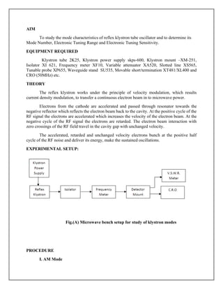
EXPERIMENTAL SETUP:
Fig.(A) Microwave bench setup for study of klystron modes
PROCEDURE
I. AM Mode
15.
1. Set theequipments as shown in figure.
2. Set up the variable attenuator at minimum position.
3. Keep the knob of klystron power supply as bellow
Mod switch – AM
Beam Voltage knob- Fully anticlockwise.
AM amplitude – around fully clockwise
AM freq. knob - around mid position.
4. Switch On the klystron power supply and cooling fan.
5. Switch ON the beam voltage/current knob and set beam current.
6. Adjust the reflector voltage knob to set maximum output in CRO.
7. Maximize the output voltage with AM amplitude and frequency
control knob of power supply.
8. Tune the plunger of klystron mount for maximum output.
9. Tune the repeller voltage knob for maximum output.
10. Tune the frequency meter and obtain the dip frequency and note
down the amplitude in the CRO.
11. Change the repeller voltage knob towards anticlockwise and
Clockwise directions and measure the amplitude of the square
wave in the oscilloscope; for each case measure the dip
frequency.
12. Repeat the step 11, and obtain the readings for other modes.
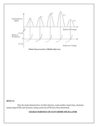
13. Plot the output magnitude Vs repeller voltage and repeller voltage
Vs dip frequency graph.
14. Calculate the ETS and ETR using the formulae
ETR = (f2 – f1) Hz and ETS = (f2 – f1) / (V2 – V1) Hz/Volts
where, f2 and f1 = dip frequencies of any two successive modes.
V2 and V1 = output amplitudes of any two successive modes.
II. FM Mode (Mode Study on the Oscilloscope)
1. Set up the equipment as shown in figure.
16.
2. Set thevariable attenuator at minimum position.
3. Keep the control knobs of klystron power supply as
Beam voltage switch - Fully anticlockwise
Modulation switch-FM
Repeller voltage knob - Fully anticlockwise
4. Switch ON the klystron power supply and cooling fan.
5. Switch ON the beam voltage/current knob and set beam current.
6. Connect the saw tooth waveform from klystron power supply
(from backside) to channel 1 and channel 2 with detector mount
probe.
7. Operate CRO in XY mode.
8. By changing the repeller voltage and amplitude of FM modulation
knob, the modes of the klystron tube can be seen on the oscilloscope.
OBSERVATIONS:
S.No. Repeller Voltage
(Volts)
Power Output
(mW)
Wave meter reading
Frequency (GHz)
17.
RESULT:
Thus the modecharacteristics of reflex klystron, mode number, transit time, electronic
tuning range (ETR) and electronic tuning sensitivity (ETS) have been determined.
CHARACTERISTICS OF GUNN DIODE OSCILLATOR
18.
AIM
To study thecharacteristics of Gunn diode oscillator and to find the threshold voltage.
EQUIPMENT REQUIRED
Gunn diode, Gunn power supply, Gunn oscillator XG-11, Isolator X1-621, frequency
meter XF-710 and Matched termination XC-400.
THEORY
The Gunn diode oscillator is based on negative differential conducting effect in bulk semi
conductor which has two conduction bands separate by an energy gap (greater than thermal
energies). A disturbance at the cathode rise to high field region which travels towards the anode.
When this field domain reaches anode, it disappears and another domain is formed at the cathode
and starts moving towards the anode and so on. The time required for domain to travel from
cathode to anode (transit time) gives oscillator frequency.
In a given oscillator the Gunn diode is placed in a resonant cavity dimension. The
oscillator frequency is determined in cavity dimension. Although Gunn oscillator can be
amplitude modulated with the bias voltage when we have used a PIN modulation in square wave
modulation of the signal coming from the Gunn diode. A measure of the square wave capability
is the modulation depth is the output ratio between ON and OFF state.
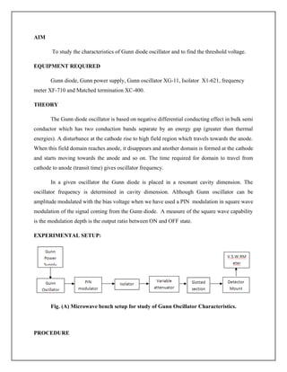
EXPERIMENTAL SETUP:
Fig. (A) Microwave bench setup for study of Gunn Oscillator Characteristics.
PROCEDURE
19.
1.Set the componentsas shown in figure.
2.Keep the control knobs of Gunn power supply as below,
i) Meter switch off
ii) Gunn bias knob –fully anticlockwise
iii) PIN diode frequency-any position.
3. Set the micrometer of Gunn oscillator for required frequency of operation.
4. Switch ON power supply
5. Measure he Gunn diode current corresponding to the various Gunn bias voltage
through the digital panel meter and meter switch do not exceed the bias voltage current.
6. Plot the voltage and current readings on the graph as shown in the Figure.
7. Measure the threshold voltage with corresponding to maintain maximum current.
20.
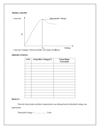
MODEL GRAPH
OBSERVATIONS:
S.No
.
Gunn BiasVoltage(V) Gunn Diode
Current(I)
RESULT
Thus the Gunn diode oscillator characteristic was obtained and its threshold voltage was
determined.
Threshold Voltage = ………………. Volts
21.
MEASUREMENT OF NUMERICALAPERTURE
AIM
The aim of the experiment is to measure the numerical aperture of the plastic fiber using
a laser source.
EQUIPMENT REQUIRED
i) Link B kit
ii) Optical fiber cable
iii) JIG
THEORY
Numerical aperture refers to the maximum angle at which light incident of the fiber end
is totally internally reflected and transmitted properly along the fiber. The cone formed by
rotation of this angle along axis of the fiber within the cone of acceptance else it is refracted out
of the fiber.
CONSIDERATIONS
1. It is very important that the optical source should be properly aligned with the cable
and distance between the launched point and cable by properly selected to ensure that the
maximum amount of optical power is transferred to the cable.
2. This experiment is best performed in a less illuminated room.
22.
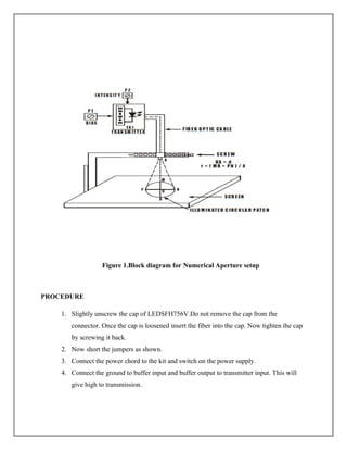
Figure 1.Block diagramfor Numerical Aperture setup
PROCEDURE
1. Slightly unscrew the cap of LEDSFH756V.Do not remove the cap from the
connector. Once the cap is loosened insert the fiber into the cap. Now tighten the cap
by screwing it back.
2. Now short the jumpers as shown.
3. Connect the power chord to the kit and switch on the power supply.
4. Connect the ground to buffer input and buffer output to transmitter input. This will
give high to transmission.
23.
5. Insert theother end of the fiber into the numerical aperture measurement. Hold the
white shut facing the fiber. Adjust the fiber such that its cut face is perpendicular to
he axis of the fiber.
6. Keep the distance of about 10mm between the fiber tip and screen. Gently tighten the
screw and thus fix the fiber in the place.
7. Now observe the illuminated circular patch of light on the screen.
8. Measure exactly the distance d and also the vertical and horizontal diameter MR and
PN as indicated in the figure.
9. Mean radius is calculated using the following formula.
10. X=(MR+PN)/4
i. 10 Find the NA of the fiber using the formula
11. NA=sin phi(max)=r/(sqrt(d2
+r2
))
12. Where phi max is the maximum angle at which the light incident is properly
transmitted through the fiber.
Tabulation:
S. No.
Height
(cm)
PN(cm) MR(cm)
Radius
(cm)
Numerical
Aperture(NA)
θmin=sin-1
(NA)
RESULT
Thus the numerical aperture of the laser was found out and the graph was plotted between the
numerical aperture and distance of fiber from the ground.
24.
PROPAGATION LOSSES ANDBENDING LOSSES IN OPTICAL FIBER
AIM
To measure propagation loss in plastic fiber provided with the lab for three different
wavelength of radiation as 950nm, 660nm and also to measure the bending loss.
APPARATUS REQUIRED
i) Kit Fiber Link-A
ii) 1Mhz Function Generator
iii) 20Mhz Dual Trace Oscilloscope
iv) 1 and 3 meter fiber cable
THEORY
Optical fibers are available in different variety of materials. These materials are usually
selected by taking into account their absorption characteristics for different wavelengths of light.
In case of optical fiber, since the signal is transmitted in the form of light which is completely
different in nature as that of electrons, one has to consider the interaction of matter with the
radiation to study the losses in fiber. Losses are introduced in fiber due to various reasons. As
light propagates from one end of fiber to another end, part of it is absorbed in the material
exhibiting absorption loss. Also part of the light is reflected back or in some other directions
from the impurity particles present in the material contributing to the loss of the signal at the
other end of the fiber. In general terms it is known as propagation loss. Plastic fibers have higher
loss of the order of 180db/km; whenever the condition for angle of incidence of the incident light
is violated the losses are introduced due to refraction of light. This occurs when fiber is subjected
to bending. Lower the radius of curvature more is the loss. Another loss is due to the coupling of
fiber at LED and photodetector ends.
PROCEDURE
1. Slightly unscrew the cap of IR LED SFH 450v.Do not remove the cap from the connector.
Once the cap is loosened, insert the fiber into the cap and assure that the fiber is properly
fixed. Now tighten the cap by screwing it back. Keep pot p8 at minimum position.
2. Make jumper connections as shown in jumper block diagram. Connect the power supply
cables with proper polarity to kit. While connecting this, ensure that the power supply is OFF.
25.
3. Connect thesignal generator between the amplifier input and ground posts of sine wave,
output to amplifier input to feed the analog signal to the preamplifier.
4. Keep the signal generator in sinewave mode and select the frequency 1khz with amplitude 2v
p-p(maximum input level is 4v p-p),or adjust voltage level if on board sinewave output is used
by pot p7. Keep switch above power connector at upper position.
5. Switch on the power supply and signal generator.
6. Check the output signal of the preamplifier at the post amplifier output. It should be same as
that of the applied input signal.
7. Now rotate the optical power control pot p6 located below power supply connector in
anticlockwise direction. This ensures minimum current flow through LED.
8. Short the following posts with the links provided, amplifier output and transmitter input.
9. Connect the other end of the fiber to detector SFH 250v very carefully as per the instructions
in step1.
10. Observe the output signal from the detector at ac output post on CRO. Adjust optical power
control pot p6.
11. We should get the reproduction of the original transmitted signal. Also adjust the amplitude
of received signal as that of the transmitted one. Mark this amplitude level as v1.
12. Now replace 1meter fiber by 3meter fiber without disturbing any of the previous settings.
Measure the amplitude level at the receiver side again. We will notice that it is less than the
previous one. Mark this as Vz.
13. If α is the attenuation of the fiber then we have,
P1/P2=V1/V2=℮^[-α (L1+L2)]
where,
α=nepers/meter
L1=fiber length for v1
L2=fiber length for
14. This α is for the wavelength of 950nm. To get the α for 660nm wavelength proceed as
follows.
15. Make use of SFH 756v and SFH 250v to perform this experiment.
26.
16. Make thejumper settings as shown in the jumper block diagram.
17. Repeat steps 1 to 12 replacing SFH 450v by SFH 756v.
18. Compare the values of α and find out the wavelength which has less attenuation in the
fiber.
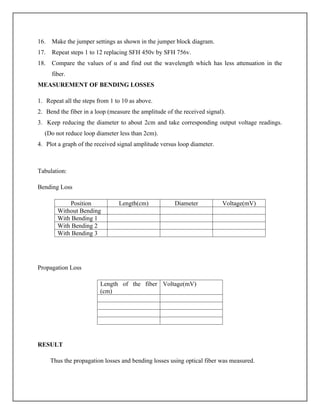
MEASUREMENT OF BENDING LOSSES
1. Repeat all the steps from 1 to 10 as above.
2. Bend the fiber in a loop (measure the amplitude of the received signal).
3. Keep reducing the diameter to about 2cm and take corresponding output voltage readings.
(Do not reduce loop diameter less than 2cm).
4. Plot a graph of the received signal amplitude versus loop diameter.
Tabulation:
Bending Loss
Position Length(cm) Diameter Voltage(mV)
Without Bending
With Bending 1
With Bending 2
With Bending 3
Propagation Loss
Length of the fiber
(cm)
Voltage(mV)
RESULT
Thus the propagation losses and bending losses using optical fiber was measured.
27.
MEASURING VSWR
AIM:
To becomefamiliar with the basic technique for measuring voltage standing wave ratio.
EQUIPMENT REQUIRED:
Klystron power supply, klystron Tube, klystron mount, Isolator, Frequency meter,
Variable attenuator, Slotted section, Tunable probe, Wave guide stands, Movable short load,
BNC cable, V.S.W.R Meter.
PROCEDURE:
Set the equipments as
Keep variable attenuator in the minimum attenuation position.
Keep the control knob of vswr meter as below.
Range db : 40 db to 50 db
Input switch : Low impedance
Meter switch : Normal position
Gain : Mid position
Keep control knobs of klystron power supply as given below:
Beam Voltage : Off
Mod-switch : AM
Beam voltage knob : Full anticlockwise
Reflector voltage knob : Full clockwise
Am amplitude knob : Full clockwise
Am frequency & amplitude knob : Mid position
Switch on the klystron power supply, vswr meter and cooling fan.
Switch on the beam voltage switch and set beam voltage at 300V
Rotate the reflector voltage knob to get deflection in vswr meter.
Tune the output by tuning the reflector voltage, amplitude and frequency of am modulation.
28.
Tune plunger ofklystron mount and probe for maximum deflection in vswr meter.
If required change the range db switch variable attenuator position and gain control knob to get
deflection in the scale of vswr meter.
As we move probe along the slotted line, the deflection will change.
(1) Measurement of low and medium VSWR
Move the probe along the slotted line to get maximum deflection in vswr meter.
Adjust the vswr meter gain control knob or variable attenuator until the meter indicates 1.0 on
normal vswr scale.
Keep all the control knobs as it is, move the probe to next minimum position. Read the vswr on
scale.
Repeat the above step for change of SS tuner probe depth and record the corresponding SWR.
If the vswr is between 3.2 and 10, change the range db to next higher position and read the vswr
on second vswr scale of 3 to 10.
(2) Measurement of high VSWR
Set the depth of SS tuner slightly more for maximum vswr.
Move the probe along with slotted line until a minimum is indicated.
Adjust the vswr gain control knob and variable attenuator to obtain a reading of 3 db in the
normal db scale ( 0 – 10db) of vswr meter.
Move the probe to the left on slotted line until full scale deflection is obtained on 0 -10 db scale.
Note and record the probe position on slotted line let it be d1.
Repeat the step 3 and then move the probe right along the slotted line until full scale deflection is
obtained on 0 – 10db normal db let it be d2.
Replace the SS tuner and termination by movable short.
Measure the distance between two successive minima positions of the probe > twice this distance
is guide wave length.
Compute vswr from the following equation.
VSWR λg / π (d1 – d2) = λg / π (Δx)
Where λg is the guide wavelength, d1 and d2 are locatimes of double minimum points.
29.
Note: this methodovercomes this effect of probe loading, since the probe is loading always
around a voltage minimum however it does not overcome the effect of detector characteristics.
For high values of VSWR, the twica – minimum method should be used. In this method the
probe is moved to a point where the power is twice the minimum. This position is denoted d – 1.
Probe is moved to the twice power point on the other side of the minimum. The position
designated as d – 2. The VSWR may be found by the relationship.
VSWR λg / π(d1 – d2)
The units of wavelength (λg) and distance are same.
CALCULATION:
LR = 20 log 10 Ei/Er = 20 log 10 1/(R)
= 20 log 10 vswr + 1/vswr-1.
VSWR = Emax / Emin
= Ei + Er / Ei – Er, -------- (1)
Where Ei = incident voltage and Er = reflected voltage
= 1 + reflection co-efficient / 1 – reflection co-efficient
Reflection co-efficient ( R) the size of reflection
R = Er/Ei = Zl – Z0 / Zl + Z0 -------- (2)
Where Zl is load impedance, Z0 is characteristic impedance
The above equation following equations
R = (vswr – 1) / (vswr + 1) -------- (3)
Note: the reflection co-efficient is expressed as a dimension less, the ratio of the voltage reflected
to the voltage incident. It must be noted that reflection co-efficient must lie between zero and
one. If reflection co-efficient is zero there is no reflection, if reflection co-efficient is one, there
is total reflection. The value of vswr is determined by the reflection co-efficient as indication in
equation – 1
30.
A. Measurement ofVSWR using VSWR Meter
Known Load Unknown Load
Movable sort SS tuner
d1(cm) D2(cm) dmin(cm) VSWR
A. Measurement of VSWR using Slotted Line Method
Known Load Unknown Load
Movable sort SS tuner
d1(cm) D2(cm) dmin(cm) dmin(cm)
RESULT:
Thus the VSWR have been measured.
31.
RADIATION PATTERN OFHORN ANTENNA
AIM
To measure the polar pattern and gain of a pyramidal horn antenna.
EQUIPMENT REQUIRED
X-band (8.2.12.4) GHz, Klystron power supply SKPS610, Klystron tube 2K25,klystron
mount XM251,Isolator XI-621, Variable attenuator XA-250, frequency meter, Pyramidal horn
antennas, Power meter-E4418B.
THEORY
Horn antenna is a rectangular waveguide with one end is stretched either in the broad
dimensions a or b. It is classified according to its construction like,
If it is prolonged in the breath a, it is known as H-plane horn antenna.
If it is stretched in width b, then it is called as H-plane horn antenna.
If it is prolonged in both directions, it is known as pyramidal horn antenna.
The measurement may be considered either in the far field distance or near field distance.
Far field distance is calculated by the formula d = 2d2
/λ0, where d is the largest dimension of the
antenna and λ0 is the free space wavelength.
Antenna measurement may be either indoor or outdoor environment. If the size of the
antenna is larger, it will give more directive radiation beam.Horn antenna is mainly used as feed
element for parabolic dish antennas ( Cassegrain feed), to increase the spill over efficiency.
PROCEDURE
1. Set up the equipments as shown in figure keeping the axis of both
antennas in same line.
2. Energize the klystron oscillator for maximum and measure the input
power.
3. Place the transmitting and receiving antenna and measure the received
32.
power.
4. Rotate thereceiving antenna and measure the power.
5. Calculate the gain for each reading.
6. Plot the values on the polar sheet.
7. From the plot determine 3dB width /beam width of the parabolid.
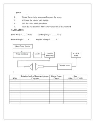
TABULATION
Input Power = …….. Watts Dip Frequency = ………. GHz
Beam Voltage = …….V Repeller Voltage = .......... V.
S.No.
Rotation Angle of Receiver Antenna
(Degrees)
Output Power
(Watts)
Gain
10 log (Po / Pi ) (dB)
33.
RESULT
Thus the gainand beam-width of the pyramidal horn antenna was measured and the polar
pattern was also drawn.
34.
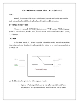
POWER DISTRIBUTION INDIRECTIONAL COUPLER
AIM
To study the power distribution in a multi-hole directional coupler and to determine its
main and auxiliary line VSWRs, Coupling factor, Directivity and S-parameters.
EQUIPMENTS REQUIRED
Klystron power supply SKPS-610, Klystron mount XM-251.Isolator XI-621, frequency
meter XF-710.Slottedline, Tunable probe, Detector mount, matched termination. MHD coupler,
VSWR meter.
THEORY
A directional coupler is a hybrid waveguide joint which couples power in an auxiliary
waveguide arm in one direction. It is a four-port device but one of the ports is terminated into a
matched load.
An ideal directional coupler has the following characteristics:
If power is fed into port(1), the power is coupled in ports(2), and (3), i.e.,
power flows in the forward direction of the auxiliary arm port (3) but no
35.
power couples inport (4), i.e., in backward direction. Similarly power fed in
(2) couples into ports(1) and (4) and not in (3).
All the four ports are matched, i.e., if there of them are terminated in
matched loads, the fourth is automatically terminated in a matched load.
If power couples in reverse direction, i.e., power fed in (1) appears in ports (2) and (4) and
nothing in (3), then such type of coupler is known as backward directional coupler. The
conclusion is that in then auxiliary section the power is only one direction.
EXPERIMENTAL SETUP:
PROCEDURE
1. Setup the components and equipments as shown in figure.
2. Energize the microwave source for a particular frequency.
3. Measure the Vmax and Vmin for corresponding ports by connecting loads to other ports.
4. Calculate the reflection co-efficient which gives the value of S-parameter.
5. Find the upper matrix values by appropriate connections.
6. From the S-parameter value calculate coupling factor, Isolation, directivity and
Insertion loss.
36.
RESULT
Thus the powerdistribution in a multi-hole directional coupler was studied. Also, its
main and auxiliary line VSWRs, Coupling factor, Directivity and S-parameters were determined.
37.
LED / LASERDIODE CHARACTERISTICS
AIM
To study the V-I characteristics of LED and plot the graph of forward current Vs output optical
energy.
EQUIPMNT REQUIRED
i) Fiber Optic Trainer kit – Link A
ii) Optical fiber cable
iii) Multi-meter
THEORY
In optical fiber communication system, electrical signal is first converted into optical signal with
the help of conversion device as LED. After this optical signal is transmitted through the optical
fiber. It is retrieved in its original device as photo detector.
Different technologies employed in chip fabrication lead to the significant variation in
parameters for various emitter diodes, data sheets for LED supply, electrical and optical
characteristics are important peak wavelength of emission conversion efficiency optical rise and
fall time which put the limitation on operating frequency, forward current through LED. Photo
detectors usually are of photoconductive, photo voltaic, transistor type and diode type output.
PROCEDURE
1. Ensure power switch is OFF and make the jumper voltage settings as per the
diagram.
2. Insert the jumper wires in JP16 and JP17 as shown.
3. Connect the ammeter, voltmeter with jumper wire connected to JP16 and JP17.
4. Keep the potentiometer Pco in its maximum position and p9 in minimum. Pco is to
control the flow of current through LED and p9 used to vary amplitude of received
signal at the phototransistor.
5. To get the V-I characteristics of LED, rotate Pco slowly and measure the forward
current ‘I’.
38.
6. Find outthe power for above readings (i.e.) power is supplied to LED from data
sheet optical power for 10mA is 200 microwatts. Efficiency is 1.15%.
7. Find the optical o/p power coupled to plastic fiber for each reading in 7th
step. Plot
the graph of forward ‘I’ to optical o/p power of LED.
8. In kit, when p9 is in minimum position 100 ohm of resistance is in series of emitter
and ground of phototransistor.
9. Connect the 30cm optical fiber cable with the kit between LED SHF750V and
phototransistor SFH350V.
10. From the transfer characteristics obtained in steps launched known in optical energy
into fiber and measure the o/p voltage at analog out terminal. Find out the current
flowing through the phototransistor with the voltage value and 100 ohm of the
resistor.
11. Repeat the steps above for various launched optical values and plot the graph for
responsivity of phototransistor. Find out the portion where detector response is
linear.
Tabulation:
S.No. Vf(v) If(mA) Pi(mW) Po(mW) V(mv) I(mA) R(A/W)
Calculation:
Pi(mW)=V*I=
Po(mW)=Pi*Vf/100=
I(mA)=V/R=
R=0.8mA*Po(mW)/10uW=
39.
RESULT
Thus the VIcharacteristics of LED was obtained
Mode characteristics of an optical fiber & digital link establishment using LED/Laser diode
40.
AIM
To Study themode characteristics of Single mode fiber
EQUIPMENT REQUIRED
iv) Link B kit
v) Optical fiber cable
vi) JIG
THEORY
Numerical aperture refers to the maximum angle at which light incident of the fiber end
is totally internally reflected and transmitted properly along the fiber. The cone formed by
rotation of this angle along axis of the fiber within the cone of acceptance else it is refracted out
of the fiber.
CONSIDERATIONS
1. It is very important that the optical source should be properly aligned with the cable
and distance between the launched point and cable by properly selected to ensure that the
maximum amount of optical power is transferred to the cable.
2. This experiment is best performed in a less illuminated room.
41.
Figure 1.Block diagramfor Numerical Aperture setup
PROCEDURE
1. Slightly unscrew the cap of LEDSFH756V.Do not remove the cap from the
connector. Once the cap is loosened insert the fiber into the cap. Now tighten the cap
by screwing it back.
2. Now short the jumpers as shown.
3. Connect the power chord to the kit and switch on the power supply.
4. Connect the ground to buffer input and buffer output to transmitter input. This will
give high to transmission.
42.
5. Insert theother end of the fiber into the numerical aperture measurement. Hold the
white shut facing the fiber. Adjust the fiber such that its cut face is perpendicular to
he axis of the fiber.
6. Keep the distance of about 10mm between the fiber tip and screen. Gently tighten the
screw and thus fix the fiber in the place.
7. Now observe the illuminated circular patch of light on the screen.
8. Measure exactly the distance d and also the vertical and horizontal diameter MR and
PN as indicated in the figure.
9. Mean radius is calculated using the following formula.
10. X=(MR+PN)/4
i. 10 Find the NA of the fiber using the formula
11. NA=sin phi(max)=r/(sqrt(d2
+r2
))
12. Where phi max is the maximum angle at which the light incident is properly
transmitted through the fiber.
Tabulation:
S. No.
Height
(cm)
PN(cm) MR(cm)
Radius
(cm)
Numerical
Aperture(NA)
θmin=sin-1
(NA)
V number –Modes of the fiber
V=πdNA / λ
d-diameter of core
λ- wavelength of source
No.of Modes =N=V2
/2
PC to PCDATA COMMUNICATION USING FIBER OPTIC SYSTEM
AIM
The objective of this experiment is to connect the RS-232 ports of two computers using Optical
Fiber Digital Link, transmit data from one computer over this link and receive the same data on
the other computer.
EQUIPMENTS REQUIRED:
Link-B Kit with power supply
Patch chords
1-Meter Fiber Cable
9 Pin D connector Cables – 2 No.s
Computers – PC, PC/XT, 386 or 486 –two No.s (Minimum Configuration)
THEORY
Microprocessor is a parallel device. It transfers the 8, 16 or 32 bit of data simultaneously over the
data lines. The number of data lines depends upon the type of microprocessor used in the system.
This is parallel I/O mode of the data transfer.
However in many situations, the parallel data transfer is either impractical or impossible. This is
very expensive and noisy especially when the distances are large. Also some devices such as
CRT or CTD are not designed for parallel I/O. Moreover in many scientific and industrial
process control applications, the devices under control are at the site or plant, which may be long
enough from control room. In these situations, the serial I/O mode is used where only one bit at a
time is transferred over a single cable. This cable may be a normal cable or an optical fiber.
Very important advantage of serial mode of data transfer is that it is inexpensive. Also the data is
accurately transferred and received in the link. It is daily practice to put checks for the data and
framing it. This plays vital role in many applications like PC-to-PC data communication,
Industrial Process controls, Robotics, CNC and DNC (Distributed numerical control) and many
more. So it is necessary to have some system, which will perform serial I/O operation between
PC and outside device using optical fiber link. And Link-B fulfills this need. It provides the
simplest and powerful way for serial communication through optical fiber. It is very easy to
install and use. Also one can enhance its flexibility through software.
HARDWARE SETTINGS
Switch off the power supply of PC. To perform this expt., the COM ports of PC are used. On
board 9-pin D-type (female) connectors are provided for interfacing with the PC. Two 9-pin
cables, with one end clamped with 9-pin D-type female connector and the other end connected to
9-pin D-type male connector, are provided with this kit. Connect D-type female connector end of
45.
one cable toone of the COM ports of PC and the 9-pin D-type connector end to CN6 (9-pin D
type connector). Similarly connect other cable to other port & CN7.
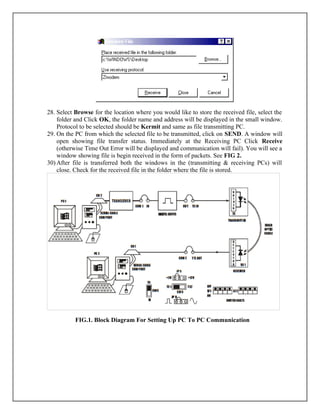
PROCEDURE:
1. Make connections as shown in fig 1. Connect the power supply cables with proper
polarity to Link-B Kit. While connecting this, ensure that the power supply is OFF.
2. Keep switch SW8 towards TX position.
3. Keep switch SW9 towards TX1 position.
4. Keep switch SW10 towards TTL position.
5. Keep Jumper JP5 towards +5V position.
6. Keep Jumpers JP6 shorted.
7. Keep Jumper JP8 towards pulse position.
8. Connect one end of the 9 to 9 pin cable to PC COM1 port and other end to CN6
connector on LINK-B kit then connect second 9 to 9 pin cable one end to second PC
COM1 port and other end to CN7 connector on LINK-B kit.
9. Switch ON the power supply.
10. Connect COM1 post on the KIT (RS-232 section) to IN post of Digital Buffer Section.
11. Connect the post OUT of Digital Buffer to the post TX IN of Transmitter.
12. Slightly unscrew the cap of LED SFH756V (660 nm) on kit. Do not remove the cap from
the connector. Once the cap is loosened, insert the one-meter fiber into the cap. Now tight
the cap by screwing it back.
13. Slightly unscrew the cap of RX1 Photo Transistor with TTL logic output SFH551V. Do
not remove the cap from the connector. Once the cap is loosened, insert the other end of
fiber into the cap. Now tighten the cap by screwing it back.
14. Connect TTL OUT post of Receiver Section to COM2 post on the KIT (RS 232
section).
15. After putting ON one of the PC, go to START MENU, PROGRAMS, ACCESSORIES,
COMMUNICATION and then Click on HYPER TERMINAL.
16. A new Window will open, where in you Double Click on HYPERTRM, Two idows will
open, one at the background and another (small window) with itle Connection
Description which will be Active.
17. Enter the name in the box by which you would like to store your connection, for e.g.
(PC2PC), and Click OK. Also you could select the Icon provided below. The background
window title will change to the name provided by you.
18. Then specify connect using: by selecting Direct to COM1 or port where your cable is
connected and then click on OK.
19. Please check the Port you have selected and the Ports you are connecting.
20. Now Window with Title COM 1 Properties will appear where Port Setting should be
done as shown below and click on OK. See FIG.
46.
21. For BitsPer Second setting you could select them for different speeds. Do ot exceed it
above 115200 bps.
22. After the above settings you click OK. The Background window will become Ative.
23. Click on File, Save As, and save it in the Directory, which you want.
24. Perform the same procedure on the other computer connected to other terminal.
25. To start communicating between the two PCs Click on the TRANSFER menu & again
click on Send File. A window will be prompted having title Send File with File Name
and Protocol. See FIG.
26. Select Browse for the file, which you would like to send to the PC connected, select the
file and Click on Open, the file name and address will be displayed in the small window.
Then select the Kermit Protocol, (optional use protocols are X modem, Y modem and
1K Xmodem.)
27. To receive the file on the PC Click on the TRANSFER Menu and again click on Receive
File. A window will be prompted having title Receive File with Location at which you
want to store the Received file and Receiving Protocol. See FIG.
47.
28. Select Browsefor the location where you would like to store the received file, select the
folder and Click OK, the folder name and address will be displayed in the small window.
Protocol to be selected should be Kermit and same as file transmitting PC.
29. On the PC from which the selected file to be transmitted, click on SEND. A window will
open showing file transfer status. Immediately at the Receiving PC Click Receive
(otherwise Time Out Error will be displayed and communication will fail). You will see a
window showing file is begin received in the form of packets. See FIG 2.
30) After file is transferred both the windows in the (transmitting & receiving PCs) will
close. Check for the received file in the folder where the file is stored.
FIG.1. Block Diagram For Setting Up PC To PC Communication
48.
FIG 2:SENDING ANDRECEIVING FILE
RESULT
Thus the PC to PC communication link using optical glass fiber and RS232
interface with the help of 1310nm laser diode was studied.
49.
Study of Connectorand splicer in optical fibers
What is the Splicing of Optical Fibers & Their Techniques
To overcome the disadvantages of optical fiber connectors, the splicing of optical fibers is used
to maintain permanent connections between the two optical fiber cables. The fiber optic cables of
various lengths like more than 5kms, 10kms, etc., are not capable of the permanent connection
and can’t run for a longer run. And also not suitable for repeated connections and disconnection
of cable connections. So, it is necessary to splice the fiber optic cables with two lengths to join
the cables together that can provide sufficient permanent connection for a longer run. This article
gives a brief description of the splicing of optical fiber cables and types.
What is the Splicing of Optical Fibers?
The splicing of optical fibers is one of the techniques used to join two optical fiber cables for
permanent connection. This technique is also known as termination or connecterization. This
method is mostly preferred when two types of cables (for example 48-fiber cable and 12-fiber
cable) are joined together for a longer run with a single length of fiber cable.
The buried optical fiber can be restored by splicing of optical fiber method. This method is
mainly used in optical communication networks for long-distance transmission of signals/data.
Splicing Techniques of Optical Fibers
There are two techniques in splicing of optical fibers depending on the insertion loss, cost, and
performance characteristics. They are fusion splicing and mechanical splicing. The mechanical
splicing is again divided into two types such as V-grooved splicing and elastic-tube splicing. The
two optical fiber cables should be aligned properly while splicing and at the same time its
geometrical factors and the mechanical strength should be considered.
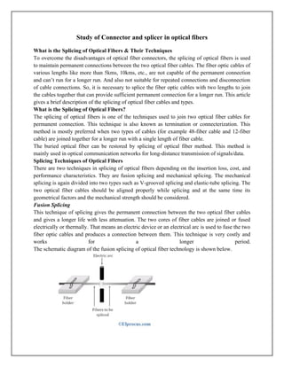
Fusion Splicing
This technique of splicing gives the permanent connection between the two optical fiber cables
and gives a longer life with less attenuation. The two cores of fiber cables are joined or fused
electrically or thermally. That means an electric device or an electrical arc is used to fuse the two
fiber optic cables and produces a connection between them. This technique is very costly and
works for a longer period.
The schematic diagram of the fusion splicing of optical fiber technology is shown below.
50.
In this method,the two fiber cables are aligned together by using a device called a fusion splicer.
So, those cables can be fused or joined together to form a connection with the help of an electric
arc more precisely. The heat produced by the electric arc can give a transparent and continuous
non-reflective connection between the two optical fiber cables with less attention, and insertion
losses. The light loss will be low in this technique. So, it is most widely used and expensive than
mechanical splicing of optical fiber cable.
The functions of the fusion splicer used in the splicing of optical fiber are,
It helps to align the optical fibers with more precision
It helps to create an electric arc or heat to fuse or join or weld the optical fibers together
This method has less attention loss of 0.1dB, and also black reflection loss is low. The
insertion losses (<0.1dB) are less in both multimode and single-mode optical fiber splicing.
The disadvantage of fusion splicing is, if excess heat is generated to melt the fiber cable for
joining, then the join would be delicate and can’t be used for a longer run.
Mechanical Splicing
This technique doesn’t require a fusion splicer to join the optical fiber together. It uses index
matching fluid to hold and align the single or more fiber cables assembled in a place to join them
together. The mechanical splicing acts as a junction to join the optical cables more precisely.
When the optical fiber cables are joined together to pass the light from one to another, the loss of
light will be low if we use the mechanical splicing technique. That means insertion loss, splicing
loss will be nearly 0.3dB. But it produces high back reflection when compared to fusion splicing.
It is very easy to repair and install for both multimode and single-mode optical fiber cables.
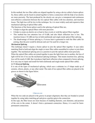
2.1 V-Grooved Splicing
It is one of the types of mechanical splicing, which uses a substrate in a V-shape made up of
ceramic, silicon, plastic, or any other metal. The ends of two optical fiber cables are placed in the
groove as shown in the figure below.
When the two ends are placed in the groove in proper alignment, then they are bonded or joined
together by using index matching gel and gives a perfect grip to the connection.
In this type, the fiber losses are more because of cladding diameter, core diameter, and position
of the core to the center. It doesn’t form a permanent connection. Hence, it is used for Semi-
permanent connections.
51.
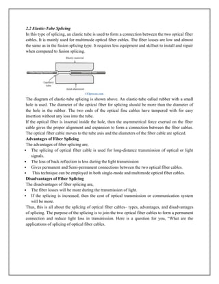
2.2 Elastic-Tube Splicing
Inthis type of splicing, an elastic tube is used to form a connection between the two optical fiber
cables. It is mainly used for multimode optical fiber cables. The fiber losses are low and almost
the same as in the fusion splicing type. It requires less equipment and skillset to install and repair
when compared to fusion splicing.
The diagram of elastic-tube splicing is shown above. An elastic-tube called rubber with a small
hole is used. The diameter of the optical fiber for splicing should be more than the diameter of
the hole in the rubber. The two ends of the optical fine cables have tampered with for easy
insertion without any loss into the tube.
If the optical fiber is inserted inside the hole, then the asymmetrical force exerted on the fiber
cable gives the proper alignment and expansion to form a connection between the fiber cables.
The optical fiber cable moves to the tube axis and the diameters of the fiber cable are spliced.
Advantages of Fiber Splicing
The advantages of fiber splicing are,
The splicing of optical fiber cable is used for long-distance transmission of optical or light
signals.
The loss of back reflection is less during the light transmission
Gives permanent and Semi-permanent connections between the two optical fiber cables.
This technique can be employed in both single-mode and multimode optical fiber cables.
Disadvantages of Fiber Splicing
The disadvantages of fiber splicing are,
The fiber losses will be more during the transmission of light.
If the splicing is increased, then the cost of optical transmission or communication system
will be more.
Thus, this is all about the splicing of optical fiber cables– types, advantages, and disadvantages
of splicing. The purpose of the splicing is to join the two optical fiber cables to form a permanent
connection and reduce light loss in transmission. Here is a question for you, “What are the
applications of splicing of optical fiber cables.
52.
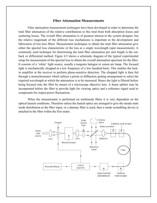
Fiber Attenuation Measurements
Fiberattenuation measurement techniques have been developed in order to determine the
total fiber attenuation of the relative contributions to this total from both absorption losses and
scattering losses. The overall fiber attenuation is of greatest interest to the system designer, but
the relative magnitude of the different loss mechanisms is important in the development and
fabrication of low-loss fibers. Measurement techniques to obtain the total fiber attenuation give
either the spectral loss characteristic or the loss at a single wavelength (spot measurement). A
commonly used technique for determining the total fiber attenuation per unit length is the cut-
back or differential method. Figure 4.5 shows a schematic diagram of the typical experimental
setup for measurement of the spectral loss to obtain the overall attenuation spectrum for the fiber.
It consists of a ‘white’ light source, usually a tungsten halogen or xenon are lamp. The focused
light is mechanically chopped at a low frequency of a few hundred hertz. This enables the lock-
in amplifier at the receiver to perform phase-sensitive detection. The chopped light is then fed
through a monochromator which utilizes a prism or diffraction grating arrangement to select the
required wavelength at which the attenuation is to be measured. Hence the light is filtered before
being focused onto the fiber by means of a microscope objective lens. A beam splitter may be
incorporated before the fiber to provide light for viewing optics and a reference signal used to
compensate for output power fluctuations.
When the measurement is performed on multimode fibers it is very dependent on the
optical launch conditions. Therefore unless the launch optics are arranged to give the steady-state
mode distribution at the fiber input, or a dummy fiber is used, then a mode scrambling device is
attached to the fiber within the first meter.
53.
The fiber isalso usually put through a cladding mode stripper, which may consist of an
S-shaped groove cut in the Teflon and filled with glycerin. This device removes light launched
into the fiber cladding through radiation into the index-matched (or slightly higher refractive
index) glycerin. A mode stripper can also be included at the fiber output end to remove any
optical power which is scattered from the core into the cladding down the fiber length. This tends
to be pronounced when the fiber cladding consists of a low refractive-index silicone resin. The
optical power at the receiving end of the fiber is detected using a p–i–n or avalanche photodiode.
In order to obtain reproducible results the photodetector surface is usually index matched to the
fiber output end face using epoxy resin or an index-matching gell. Finally, the electrical output
from the photodetector is fed to a lock-in amplifier, the output of which is recorded. The cut-
back method* involves taking a set of optical output power measurements over the required
spectrum using a long length of fiber (usually at least a kilometer). This fiber is generally
uncabled having only a primary protective coating. Increased losses due to cabling do not tend to
change the shape of the attenuation spectrum as they are entirely radiative, and for multimode
fibers are almost wavelength independent. The fiber is then cut back to a point 2 m from the
input end and, maintaining the same launch conditions, another set of power output
measurements is taken.
L1 and L2 are the original and cut-back fiber lengths respectively, and P01 and P02 are
the corresponding output optical powers at a specific wavelength from the original and cut-back
fiber lengths. Hence when L1 and L2 are measured in kilometers, α dB has units of dB km−1.
Where V1 and V2 correspond to output voltage readings from the original fiber length
and the cut-back fiber length respectively.


![3. Connect the signal generator between the amplifier input and ground posts of sine wave,
output to amplifier input to feed the analog signal to the preamplifier.
4. Keep the signal generator in sinewave mode and select the frequency 1khz with amplitude 2v
p-p(maximum input level is 4v p-p),or adjust voltage level if on board sinewave output is used
by pot p7. Keep switch above power connector at upper position.
5. Switch on the power supply and signal generator.
6. Check the output signal of the preamplifier at the post amplifier output. It should be same as
that of the applied input signal.
7. Now rotate the optical power control pot p6 located below power supply connector in
anticlockwise direction. This ensures minimum current flow through LED.
8. Short the following posts with the links provided, amplifier output and transmitter input.
9. Connect the other end of the fiber to detector SFH 250v very carefully as per the instructions
in step1.
10. Observe the output signal from the detector at ac output post on CRO. Adjust optical power
control pot p6.
11. We should get the reproduction of the original transmitted signal. Also adjust the amplitude
of received signal as that of the transmitted one. Mark this amplitude level as v1.
12. Now replace 1meter fiber by 3meter fiber without disturbing any of the previous settings.
Measure the amplitude level at the receiver side again. We will notice that it is less than the
previous one. Mark this as Vz.
13. If α is the attenuation of the fiber then we have,
P1/P2=V1/V2=℮^[-α (L1+L2)]
where,
α=nepers/meter
L1=fiber length for v1
L2=fiber length for
14. This α is for the wavelength of 950nm. To get the α for 660nm wavelength proceed as
follows.
15. Make use of SFH 756v and SFH 250v to perform this experiment.](https://image.slidesharecdn.com/opticalandmicrowavelabmanual-251109180925-5251c800/85/19EC704-Optical-and-Microwave-Lab-Manual-docx-25-320.jpg)


![Ece ppt[1]](https://cdn.slidesharecdn.com/ss_thumbnails/eceppt1-120602041335-phpapp02-thumbnail.jpg?width=640&height=640&fit=bounds)