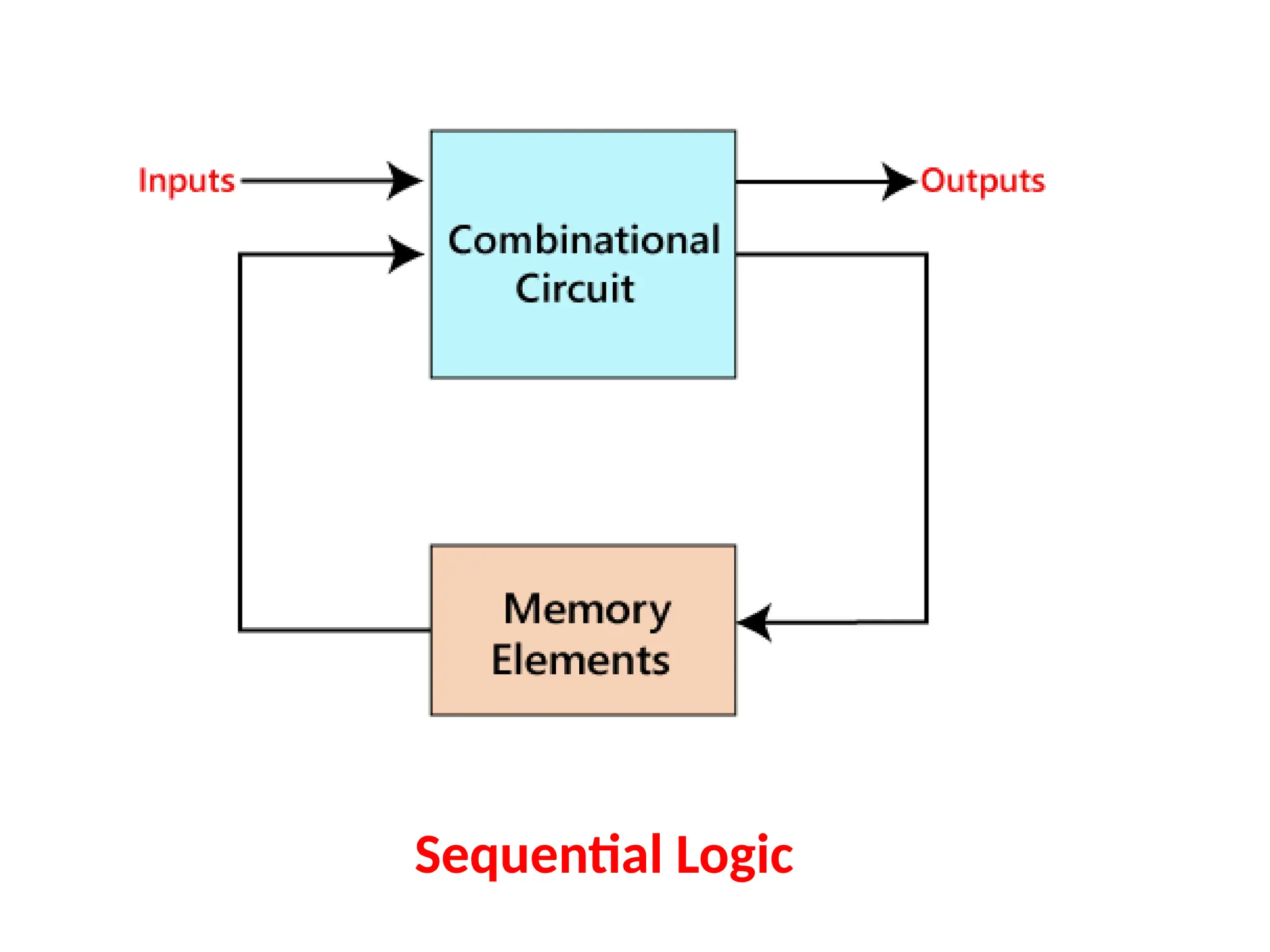
Sequential Circuits
• Logiccircuit Outputs depend not only on the present inputs,
but also on the past history(outputs) of the system.
• The system memorizes the state in which it is in.
• How does the circuit memorize state?
• Using basic memory elements called latches and flip-flops.
• In practice, we need something more. We should be able to
set the output values to 0 or 1 as per our requirement.
• Need some additional circuitry.
• The exact functionality distinguishes between different
types of latches and flip-flops.
Types of SequentialCircuits
There are two types:
1. Asynchronous sequential circuits
The clock signals are not used by the Asynchronous sequential
circuits. The asynchronous circuit is operated through the pulses.
So, the changes in the input can change the state of the circuit.
The asynchronous circuits do not use clock pulses.
2. Synchronous sequential circuits
In synchronous sequential circuits, synchronization of the memory
element's state is done by the clock signal. The output is stored in
either flip-flops or latches(memory devices). The synchronization of
the outputs is done with either only negative edges of the clock
signal or only positive edges.
4.
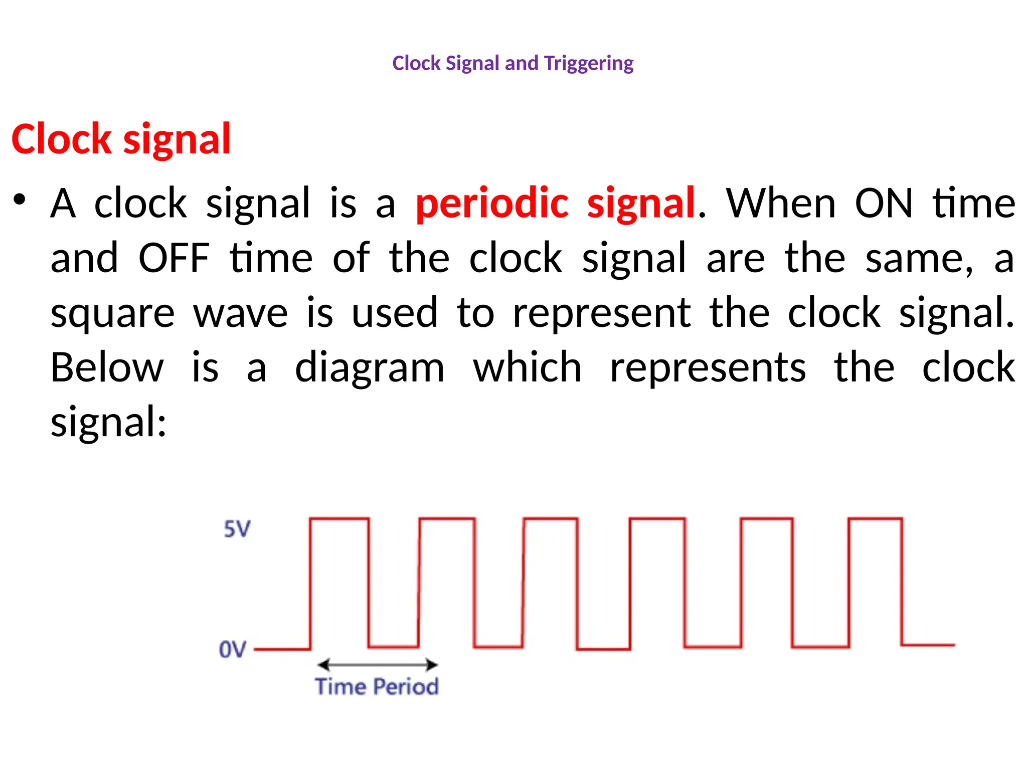
Clock Signal andTriggering
Clock signal
• A clock signal is a periodic signal. When ON time
and OFF time of the clock signal are the same, a
square wave is used to represent the clock signal.
Below is a diagram which represents the clock
signal:
5.
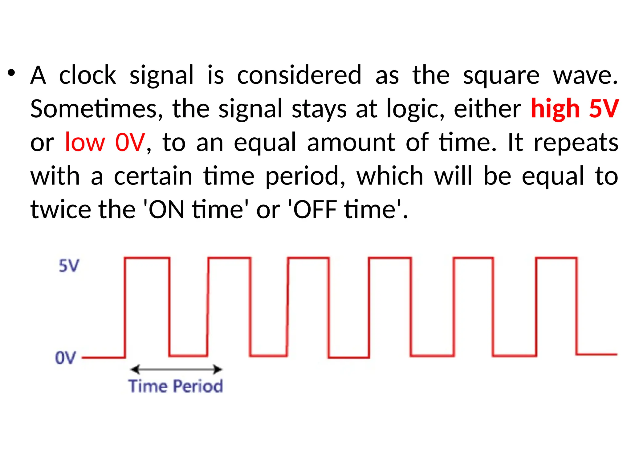
• A clocksignal is considered as the square wave.
Sometimes, the signal stays at logic, either high 5V
or low 0V, to an equal amount of time. It repeats
with a certain time period, which will be equal to
twice the 'ON time' or 'OFF time'.
6.
Types of Triggering
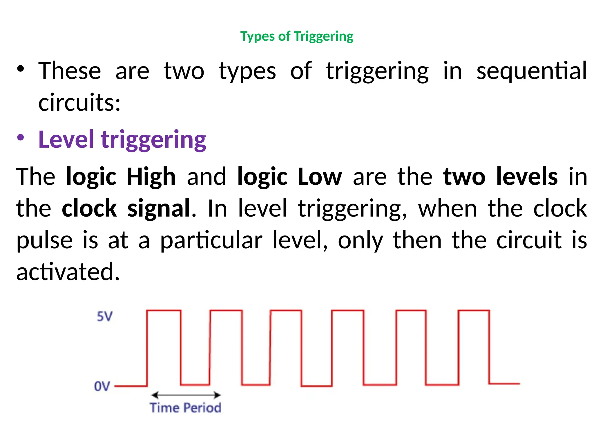
•These are two types of triggering in sequential
circuits:
• Level triggering
The logic High and logic Low are the two levels in
the clock signal. In level triggering, when the clock
pulse is at a particular level, only then the circuit is
activated.
7.
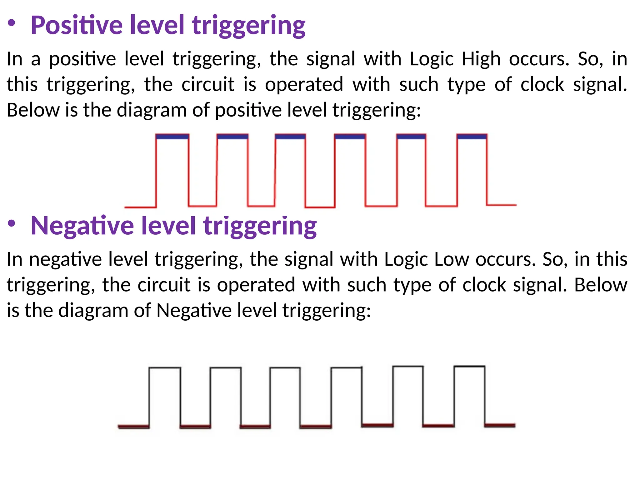
• Positive leveltriggering
In a positive level triggering, the signal with Logic High occurs. So, in
this triggering, the circuit is operated with such type of clock signal.
Below is the diagram of positive level triggering:
• Negative level triggering
In negative level triggering, the signal with Logic Low occurs. So, in this
triggering, the circuit is operated with such type of clock signal. Below
is the diagram of Negative level triggering:
8.
Edge triggering
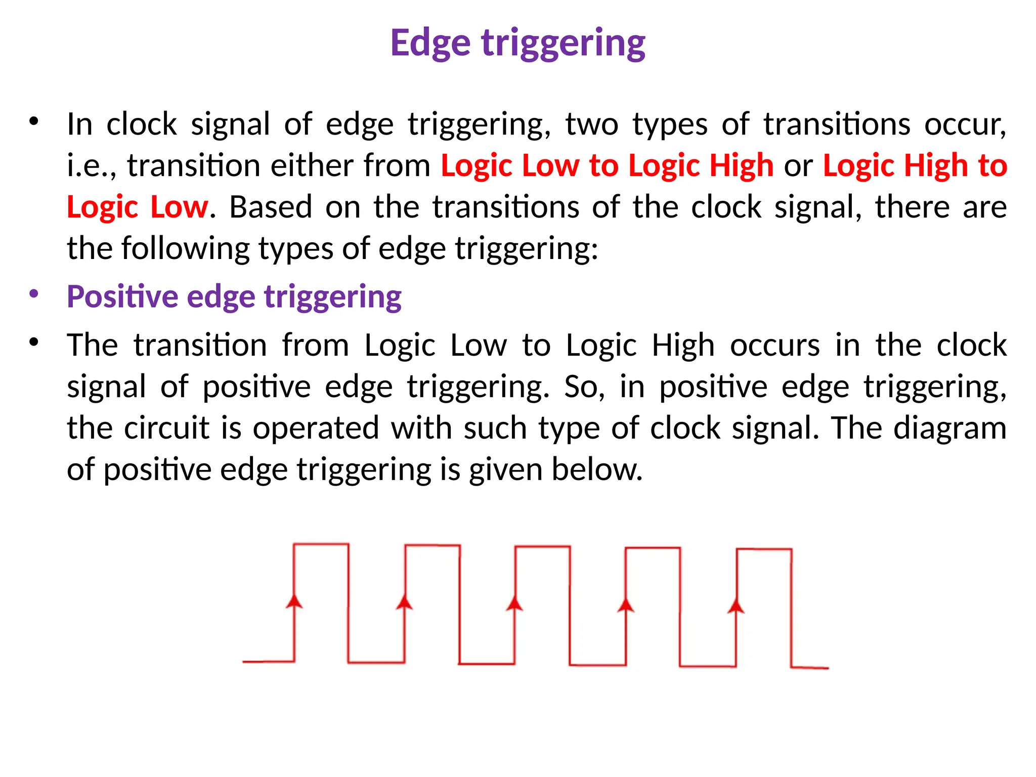
• Inclock signal of edge triggering, two types of transitions occur,
i.e., transition either from Logic Low to Logic High or Logic High to
Logic Low. Based on the transitions of the clock signal, there are
the following types of edge triggering:
• Positive edge triggering
• The transition from Logic Low to Logic High occurs in the clock
signal of positive edge triggering. So, in positive edge triggering,
the circuit is operated with such type of clock signal. The diagram
of positive edge triggering is given below.
9.
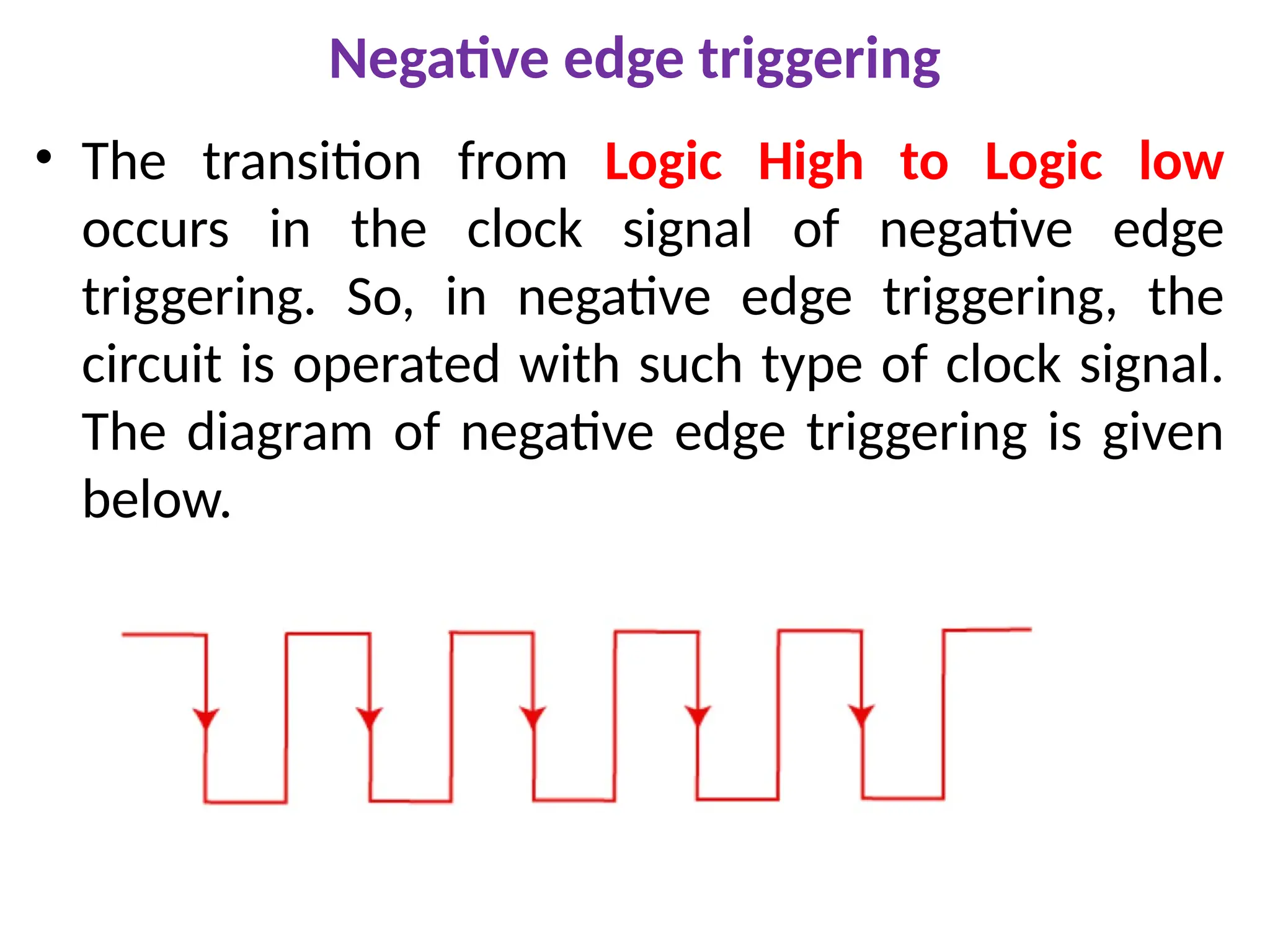
Negative edge triggering
•The transition from Logic High to Logic low
occurs in the clock signal of negative edge
triggering. So, in negative edge triggering, the
circuit is operated with such type of clock signal.
The diagram of negative edge triggering is given
below.
10.
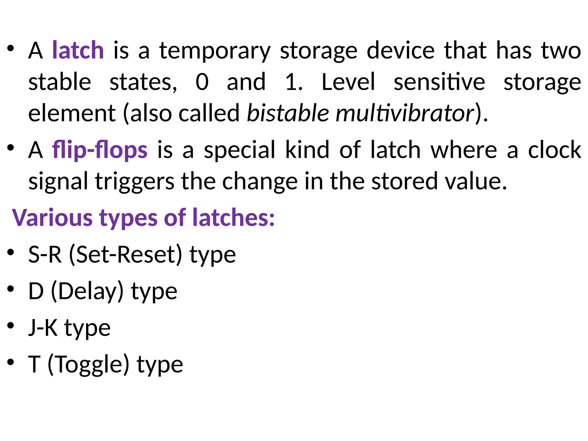
• A latchis a temporary storage device that has two
stable states, 0 and 1. Level sensitive storage
element (also called bistable multivibrator).
• A flip-flops is a special kind of latch where a clock
signal triggers the change in the stored value.
Various types of latches:
• S-R (Set-Reset) type
• D (Delay) type
• J-K type
• T (Toggle) type
11.
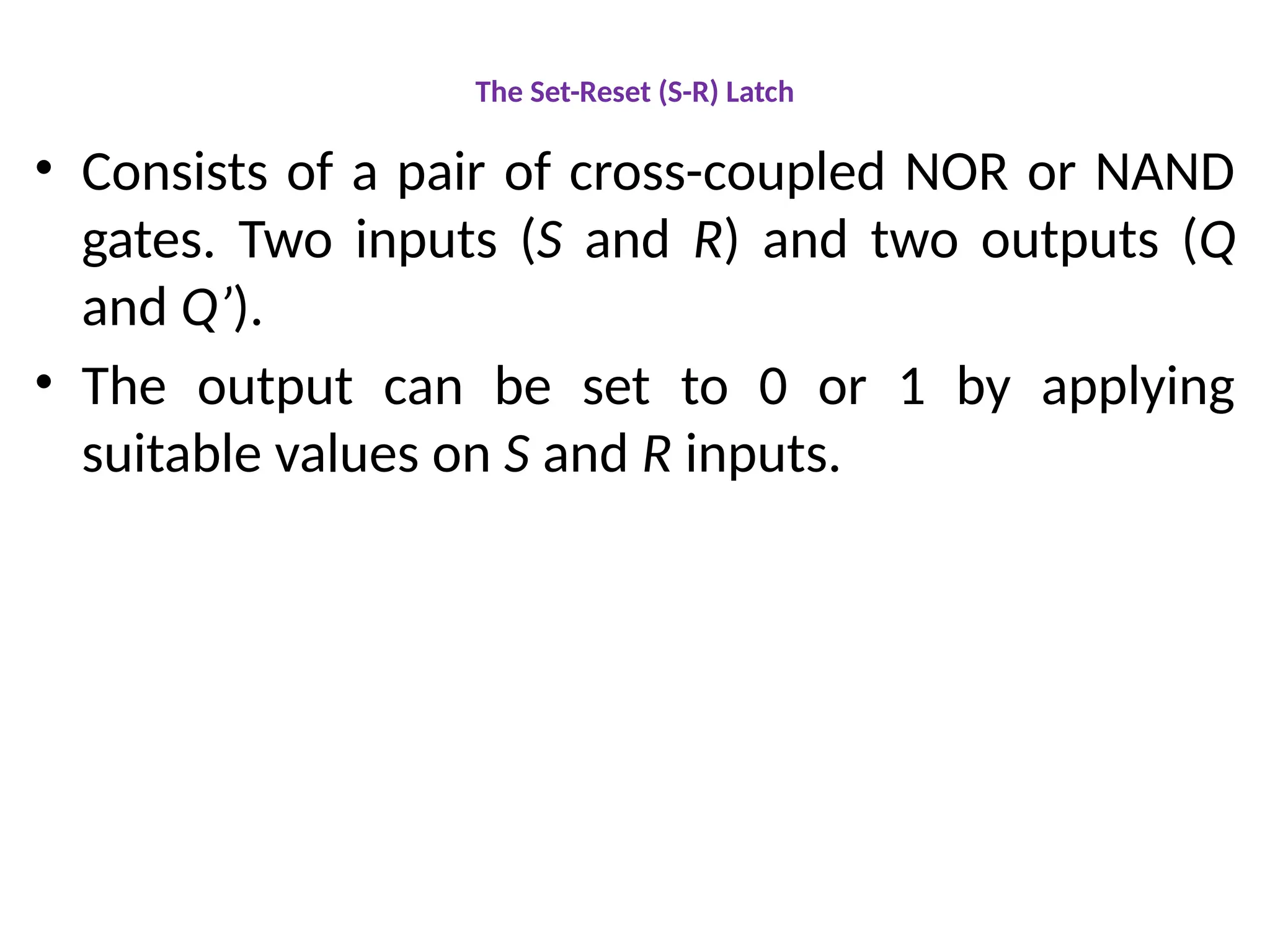
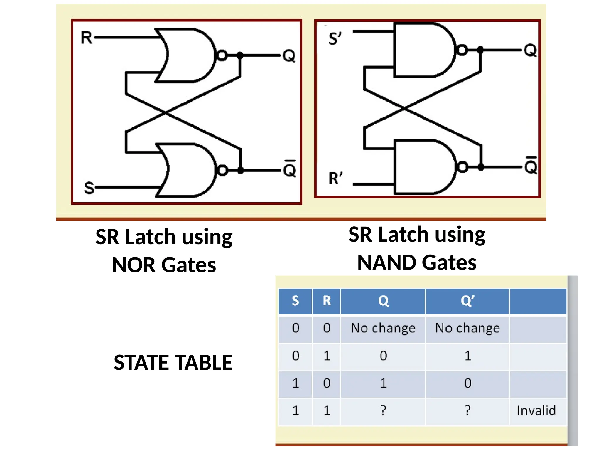
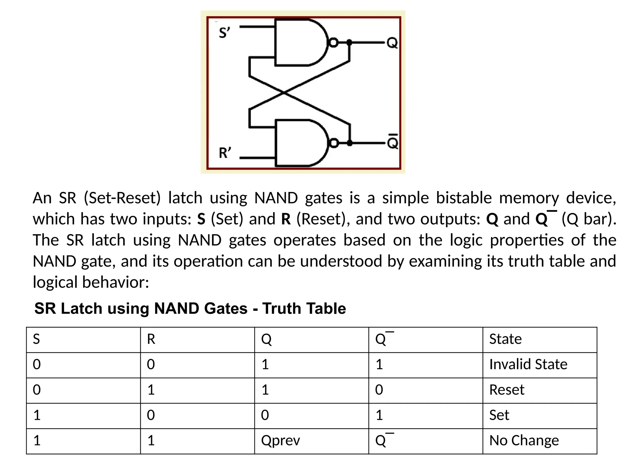
The Set-Reset (S-R)Latch
• Consists of a pair of cross-coupled NOR or NAND
gates. Two inputs (S and R) and two outputs (Q
and Q’).
• The output can be set to 0 or 1 by applying
suitable values on S and R inputs.
An SR (Set-Reset)latch using NAND gates is a simple bistable memory device,
which has two inputs: S (Set) and R (Reset), and two outputs: Q and Q‾(Q bar).
The SR latch using NAND gates operates based on the logic properties of the
NAND gate, and its operation can be understood by examining its truth table and
logical behavior:
S R Q Q‾ State
0 0 1 1 Invalid State
0 1 1 0 Reset
1 0 0 1 Set
1 1 Qprev Q‾ No Change
SR Latch using NAND Gates - Truth Table
14.
• Explanation ofOperation:
• Set State (S = 1, R = 0):
– The output Q is set to 1.
– Q‾becomes 0.
– This means the latch is in the Set state, where Q stores a high value.
• Reset State (S = 0, R = 1):
– The output Q is set to 0.
– Q‾Qbecomes 1.
– This is the Reset state, where Q stores a low value.
• No Change (S = 1, R = 1):
– The outputs remain at their previous values (Qprev and Q‾
prev).
– This is called the latched state, where the latch holds its previous state.
• Invalid State (S = 0, R = 0):
– Both Q and Q‾go to 1, which violates the logic of the circuit (Q and Q‾
are supposed to be complements).
– This is considered an invalid or undefined state, and it is avoided in
practical use.
15.
Race condition:
• Ascenario where the final result or output
depends on the relative speeds of various
components (here gates).
• If we apply S = R = 1, and then apply S = R = 0, the
outputs will settle to either Q = 0, Q’ = 1 or Q = 1, Q’ =
0 depending on the relative speeds of the two gates.
16.
• When J=1,K=1, Toggle i.e Q’n
• For JK flip-flop if J, K and Clock are equal to 1 the
state of flip-flop keeps on toggling which leads to
uncertainty in determining the output of the
flipflop.
• This problem is called Race around the condition.
This can be avoided by
❖ Using Edge triggering of JK Flip Flop
❖ Enhancing the propagation delay
❖ Using Master-Slave Flip Flop
17.
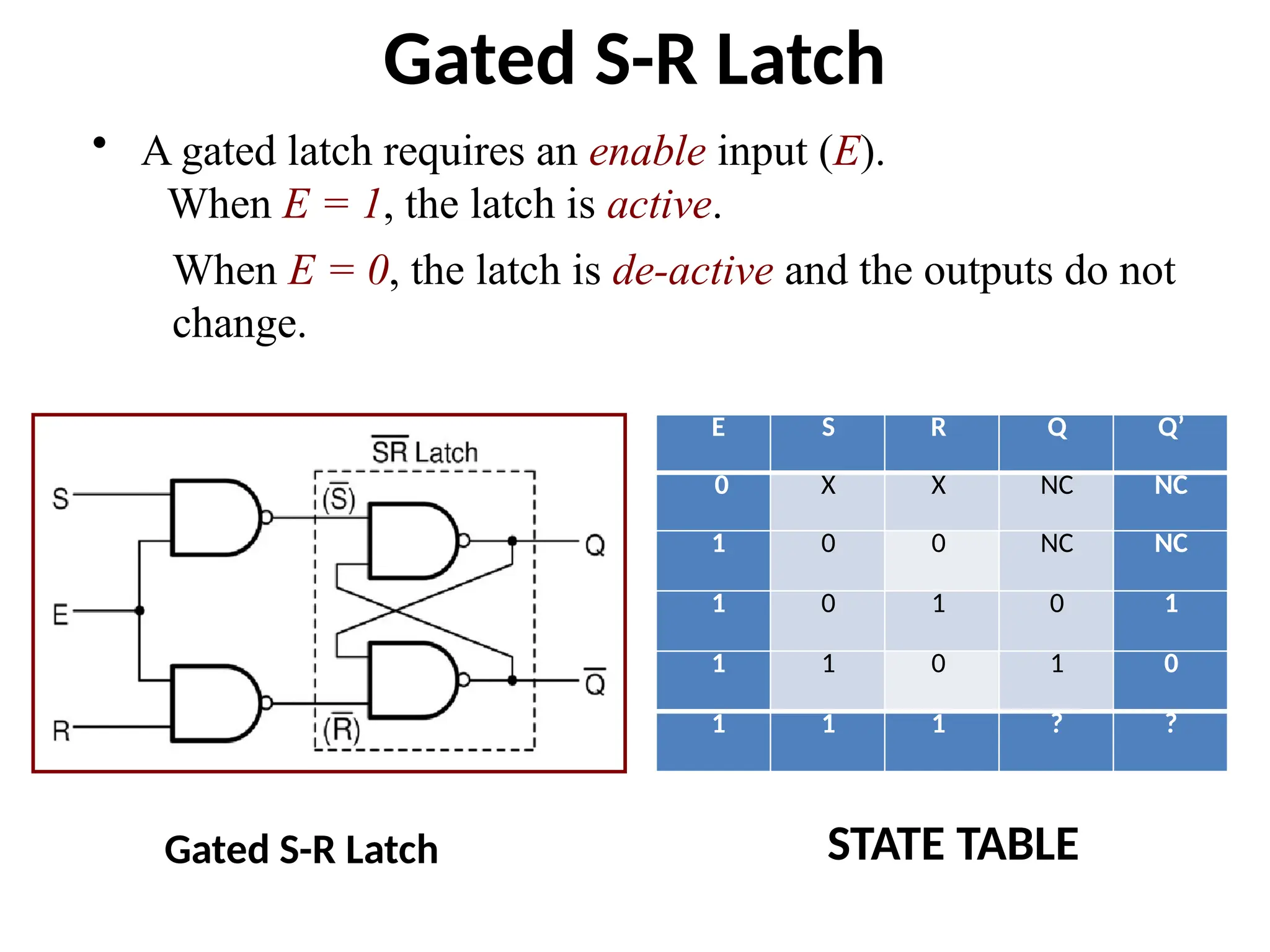
Gated S-R Latch
ES R Q Q’
0 X X NC NC
1 0 0 NC NC
1 0 1 0 1
1 1 0 1 0
1 1 1 ? ?
When E = 0, the latch is de-active and the outputs do not
change.
• A gated latch requires an enable input (E).
When E = 1, the latch is active.
STATE TABLE
Gated S-R Latch