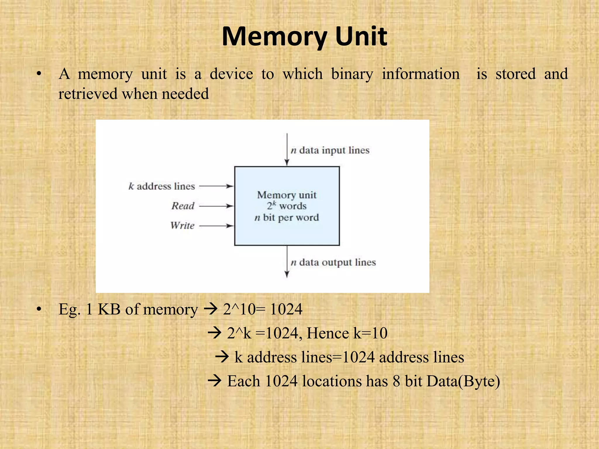
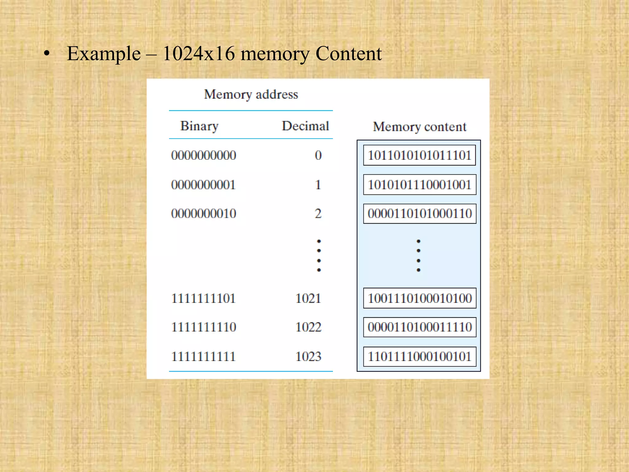
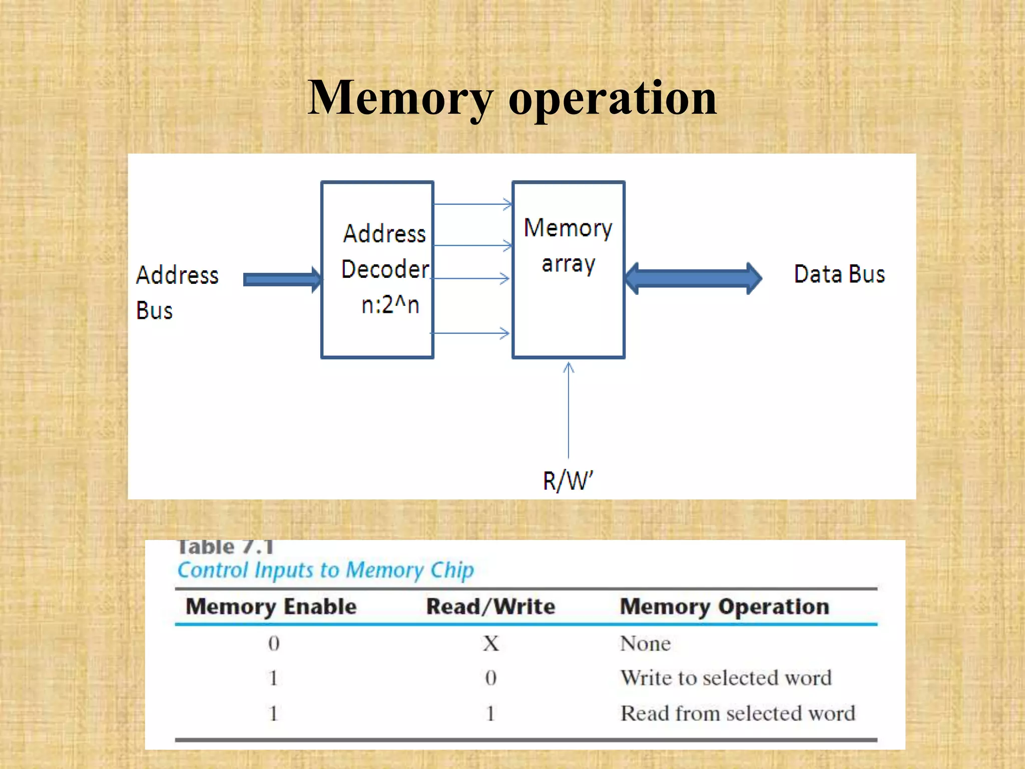
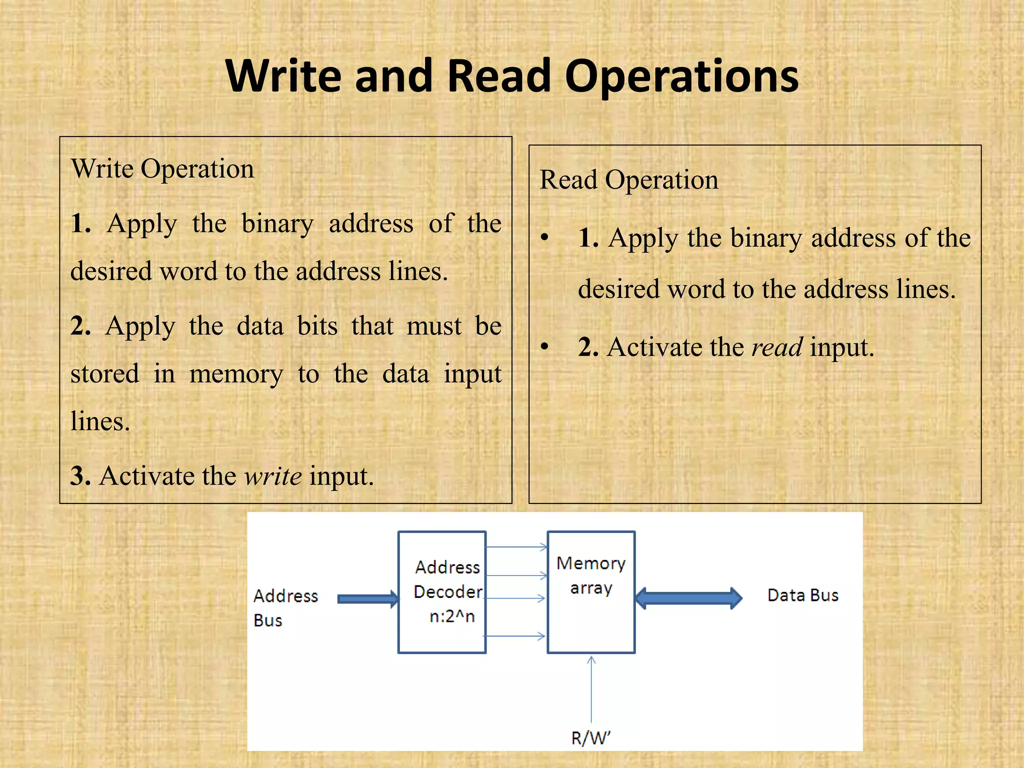
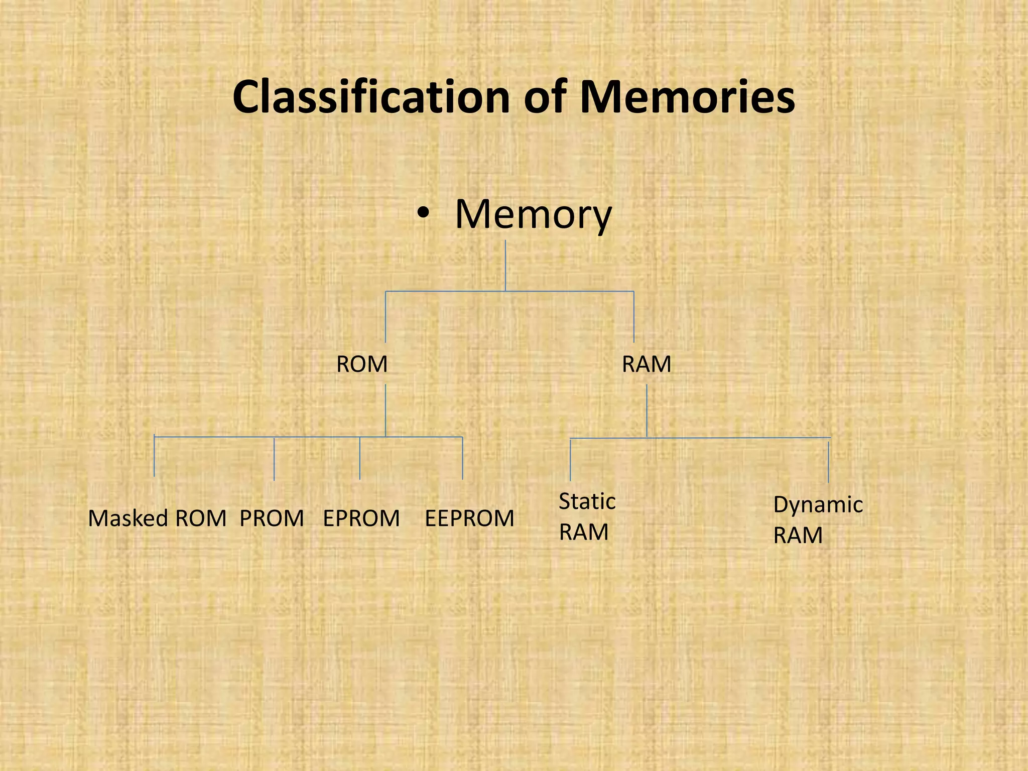
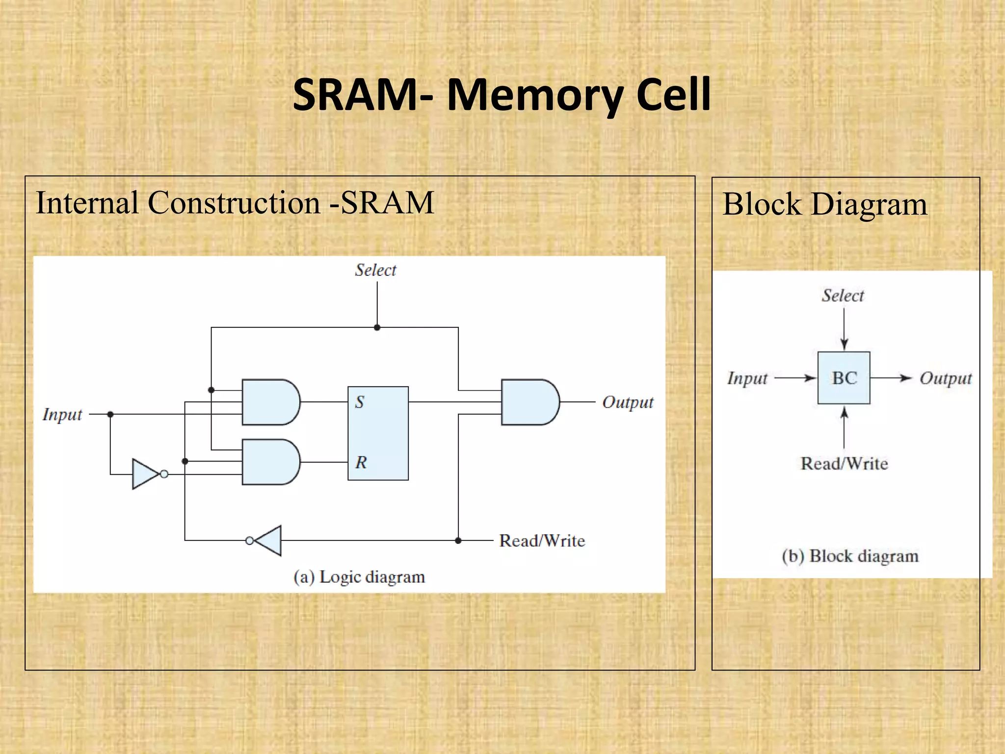
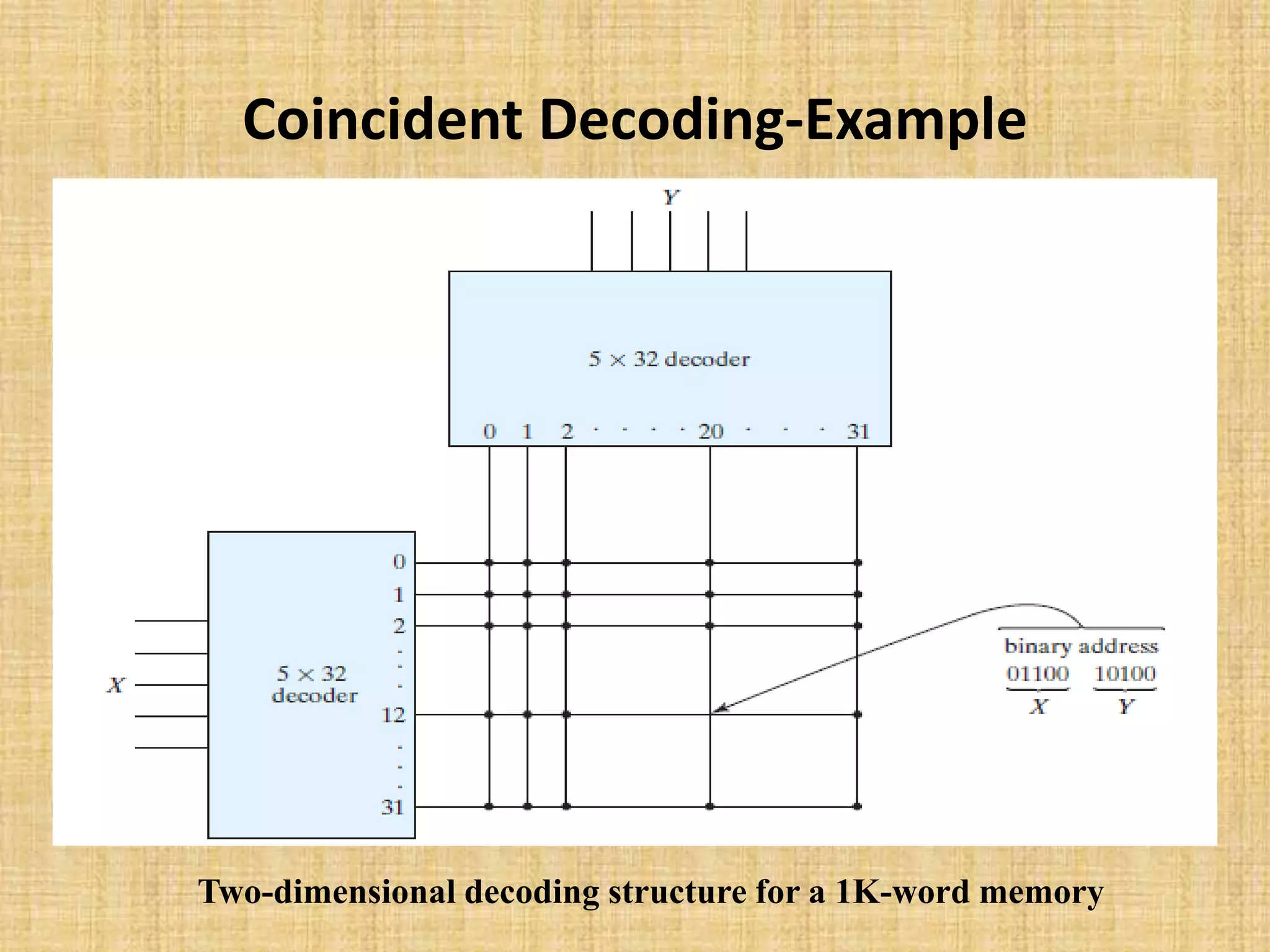
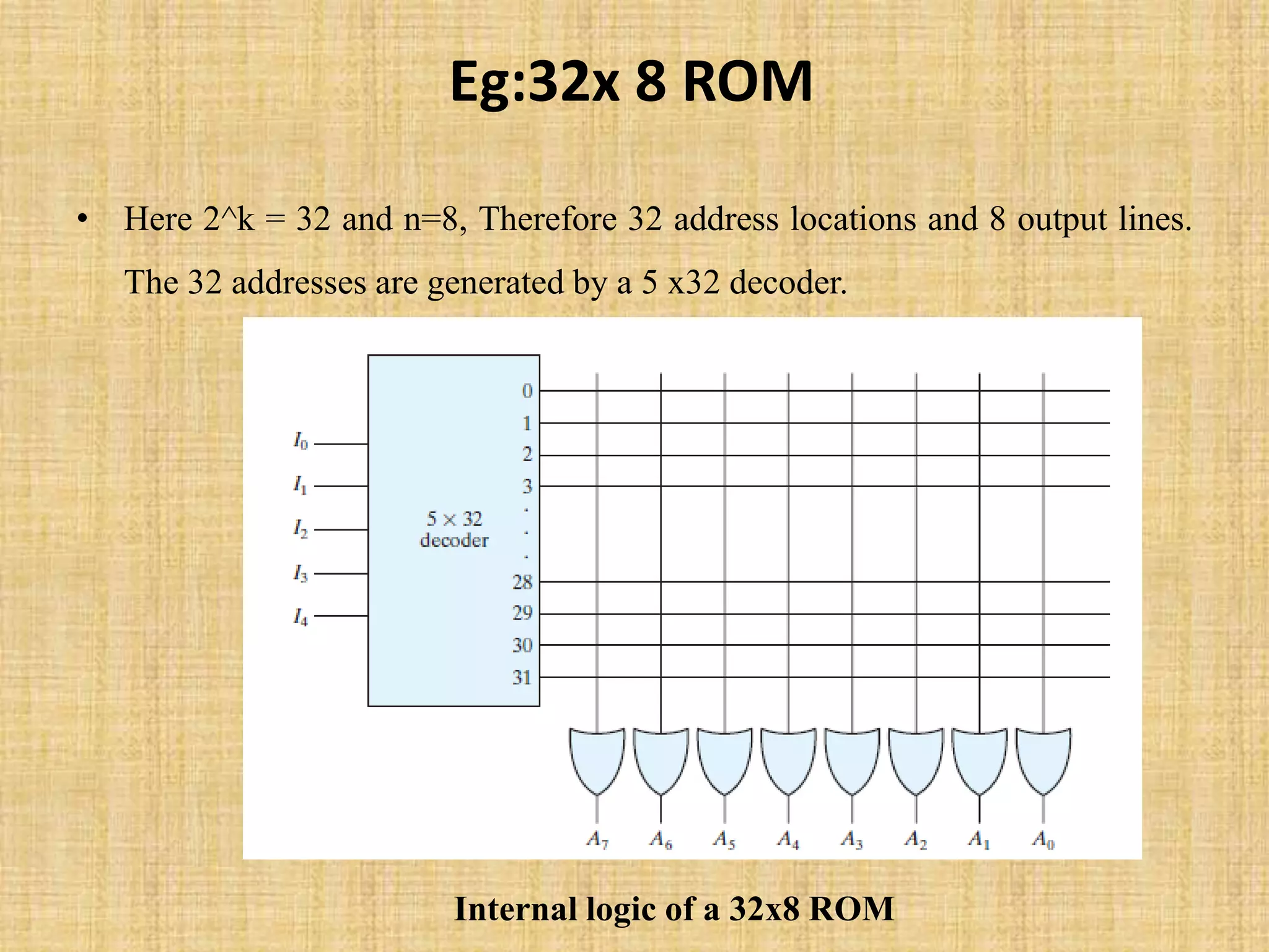
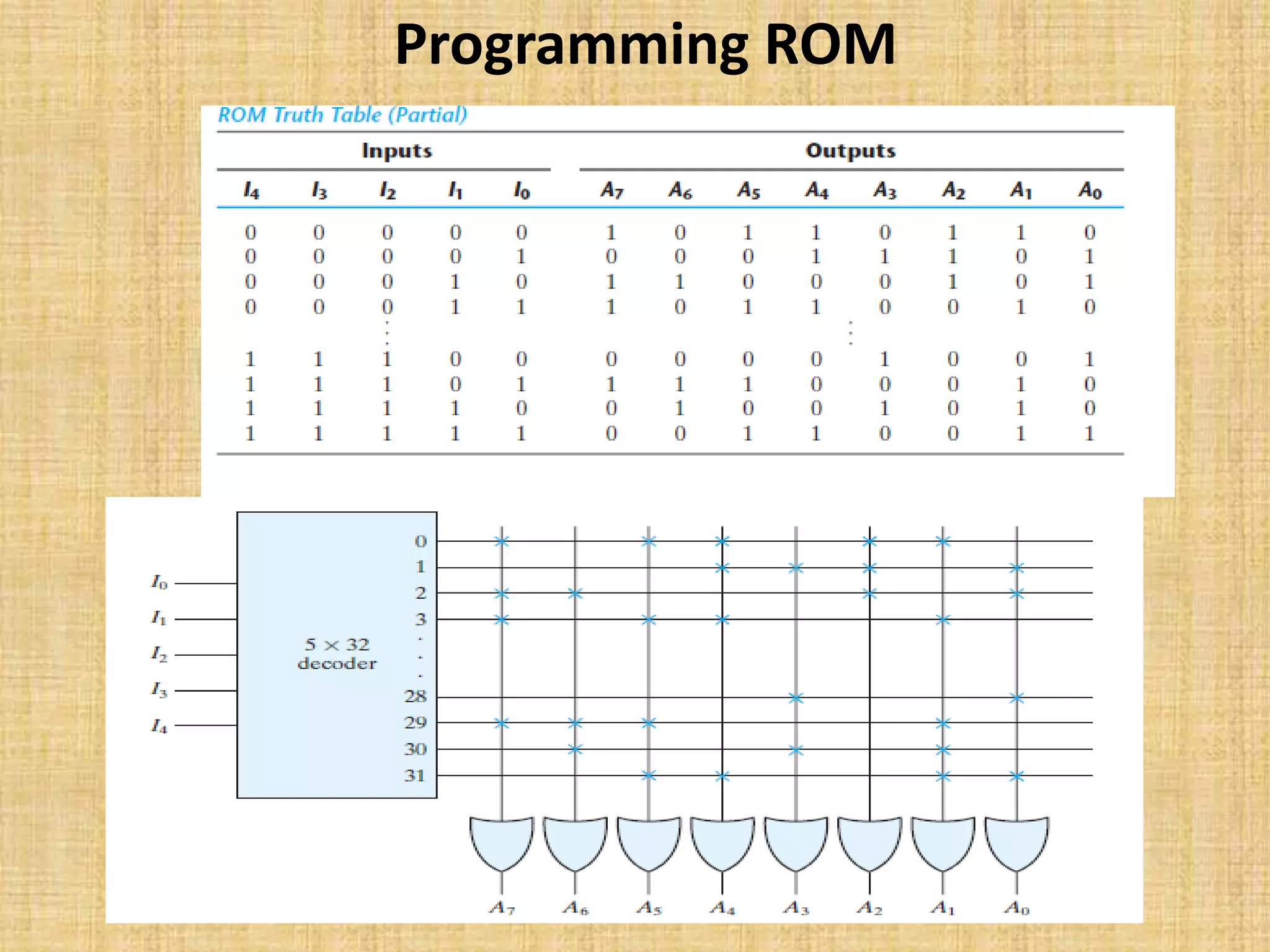
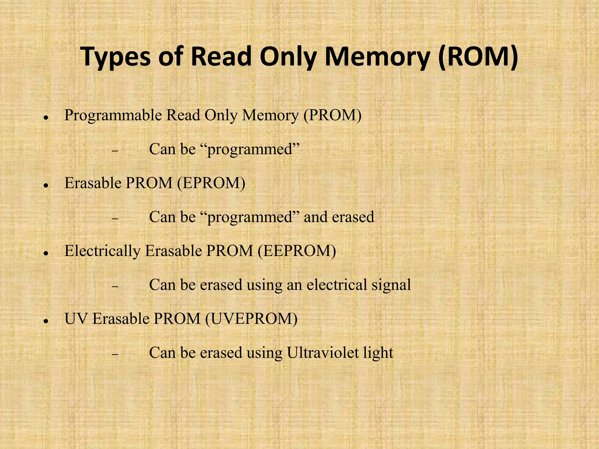
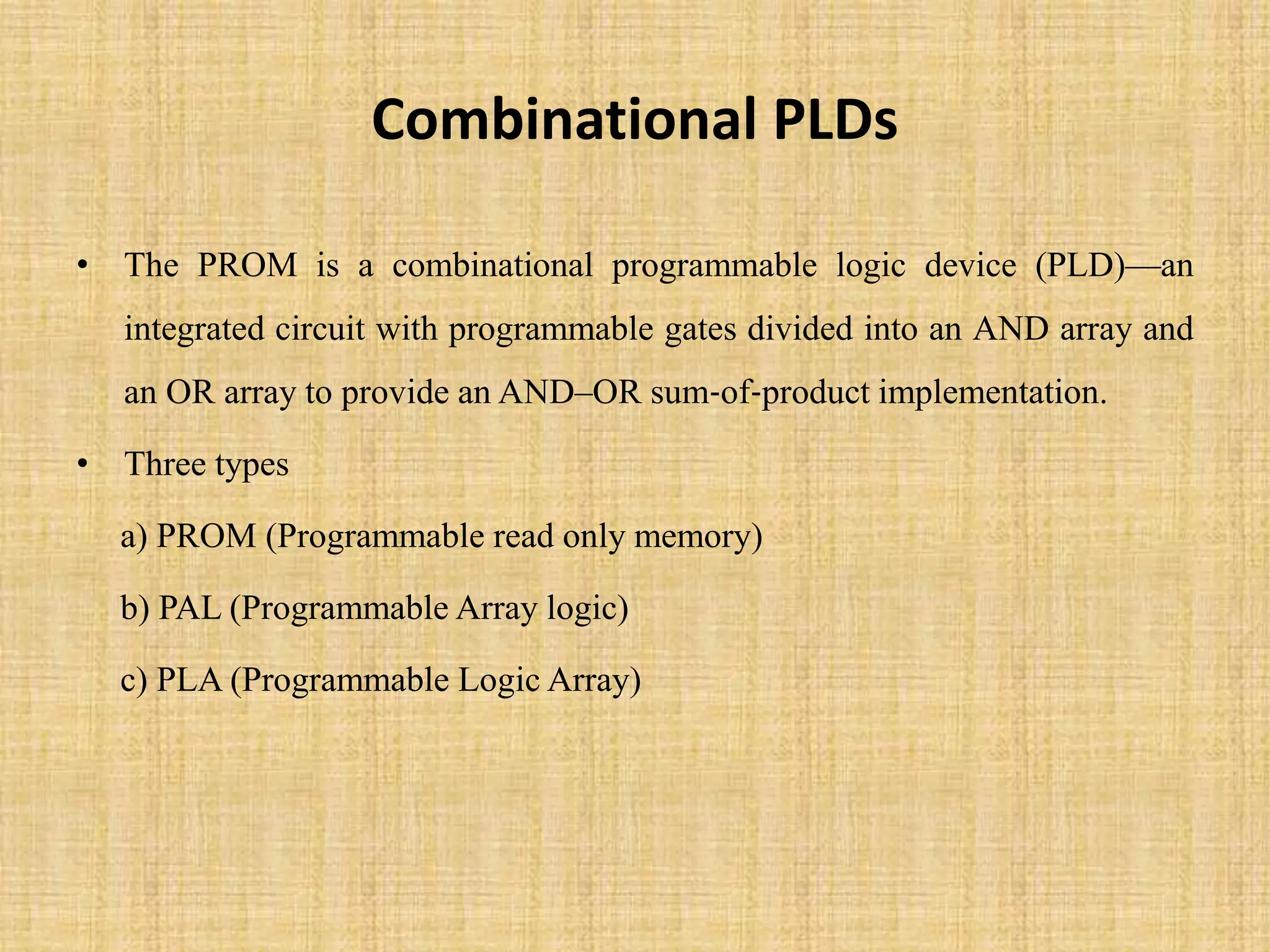
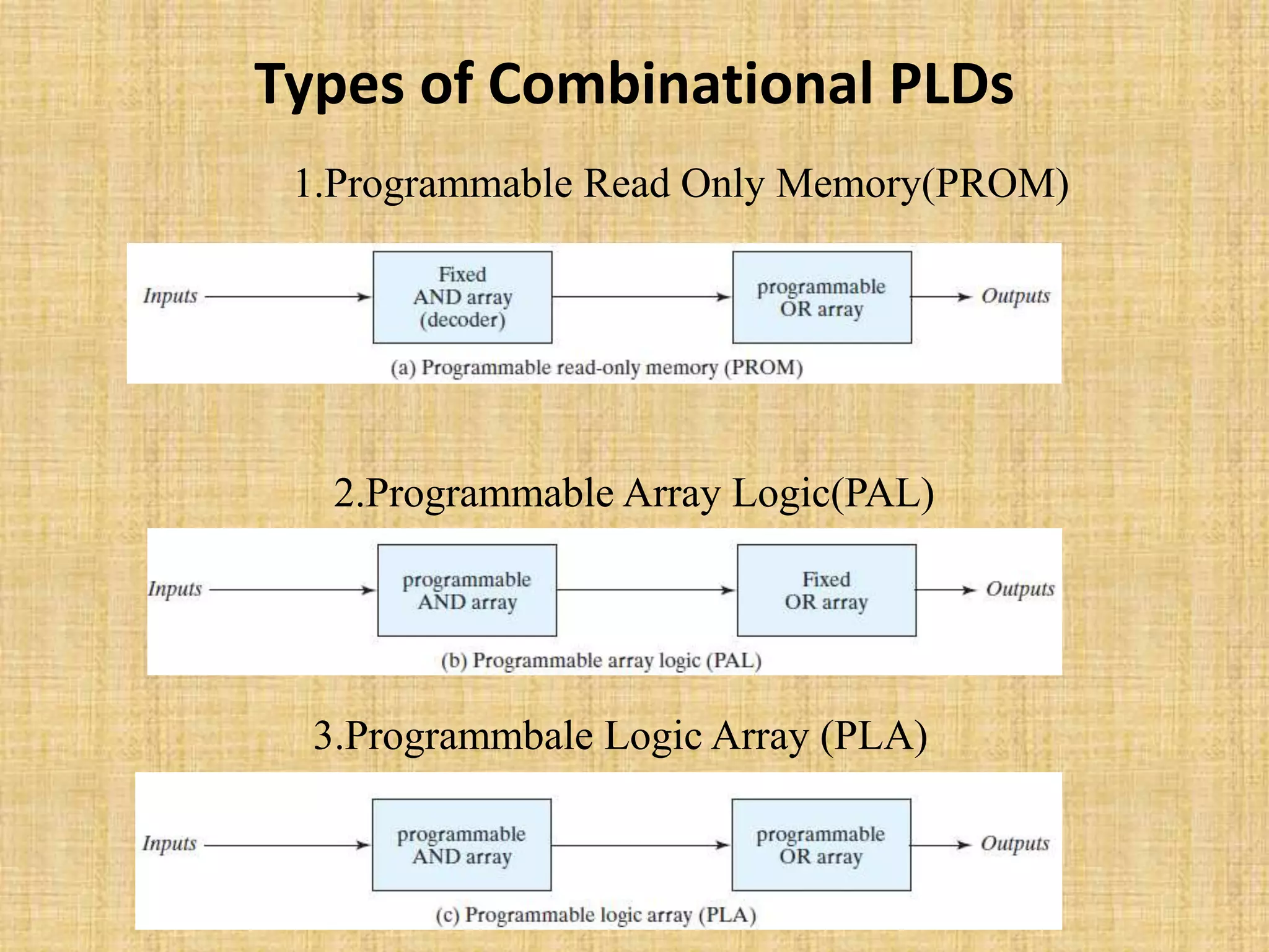
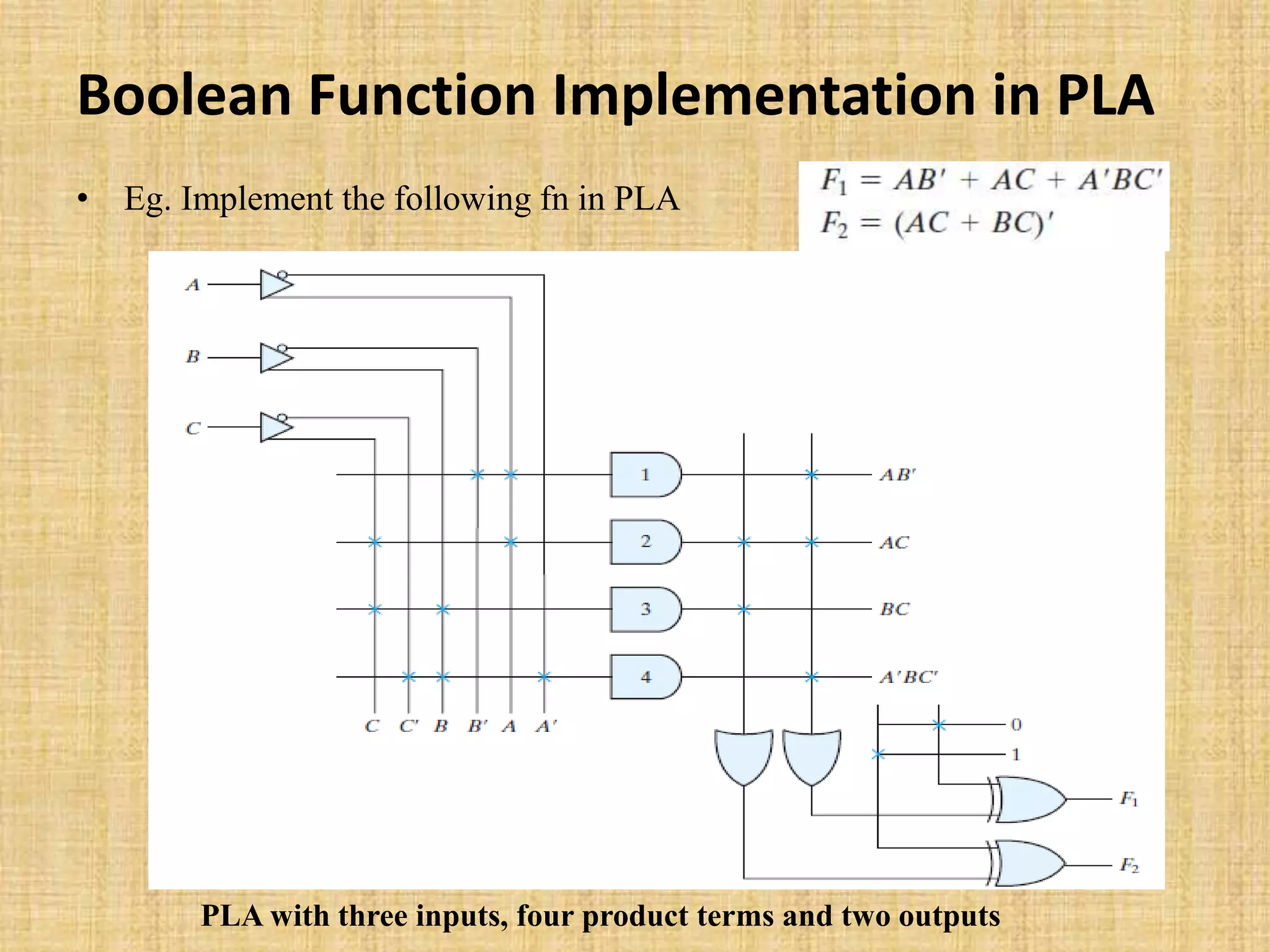
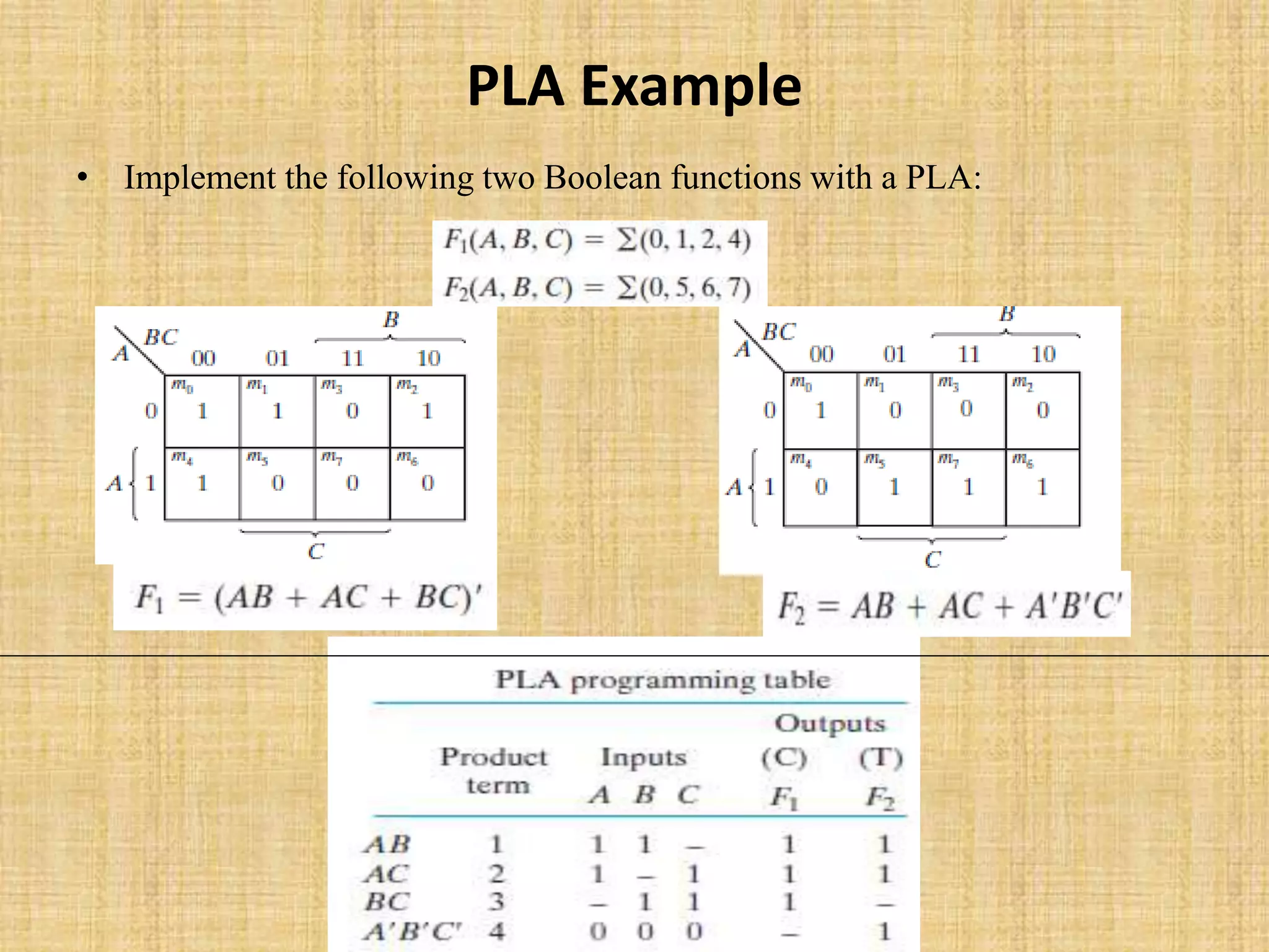
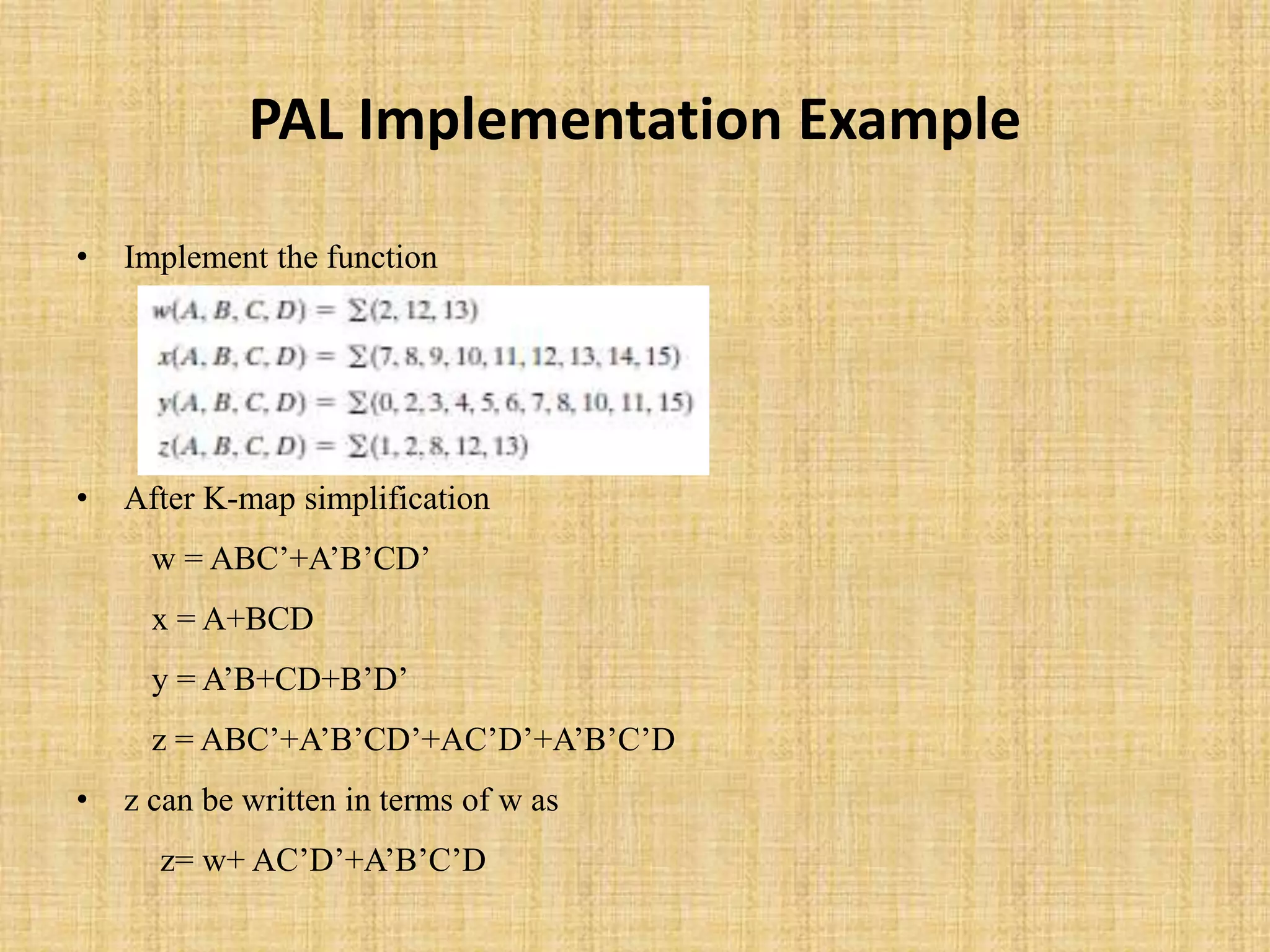
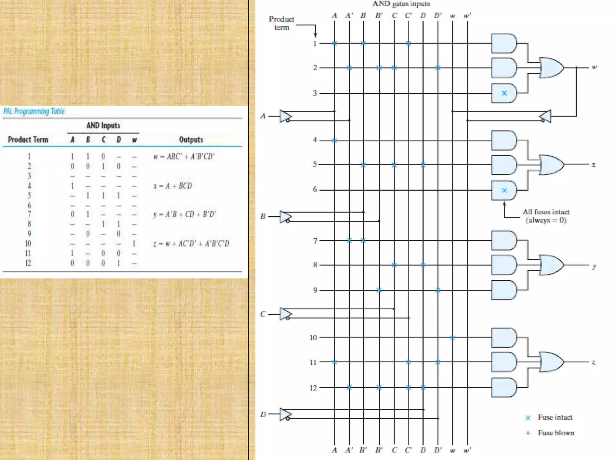
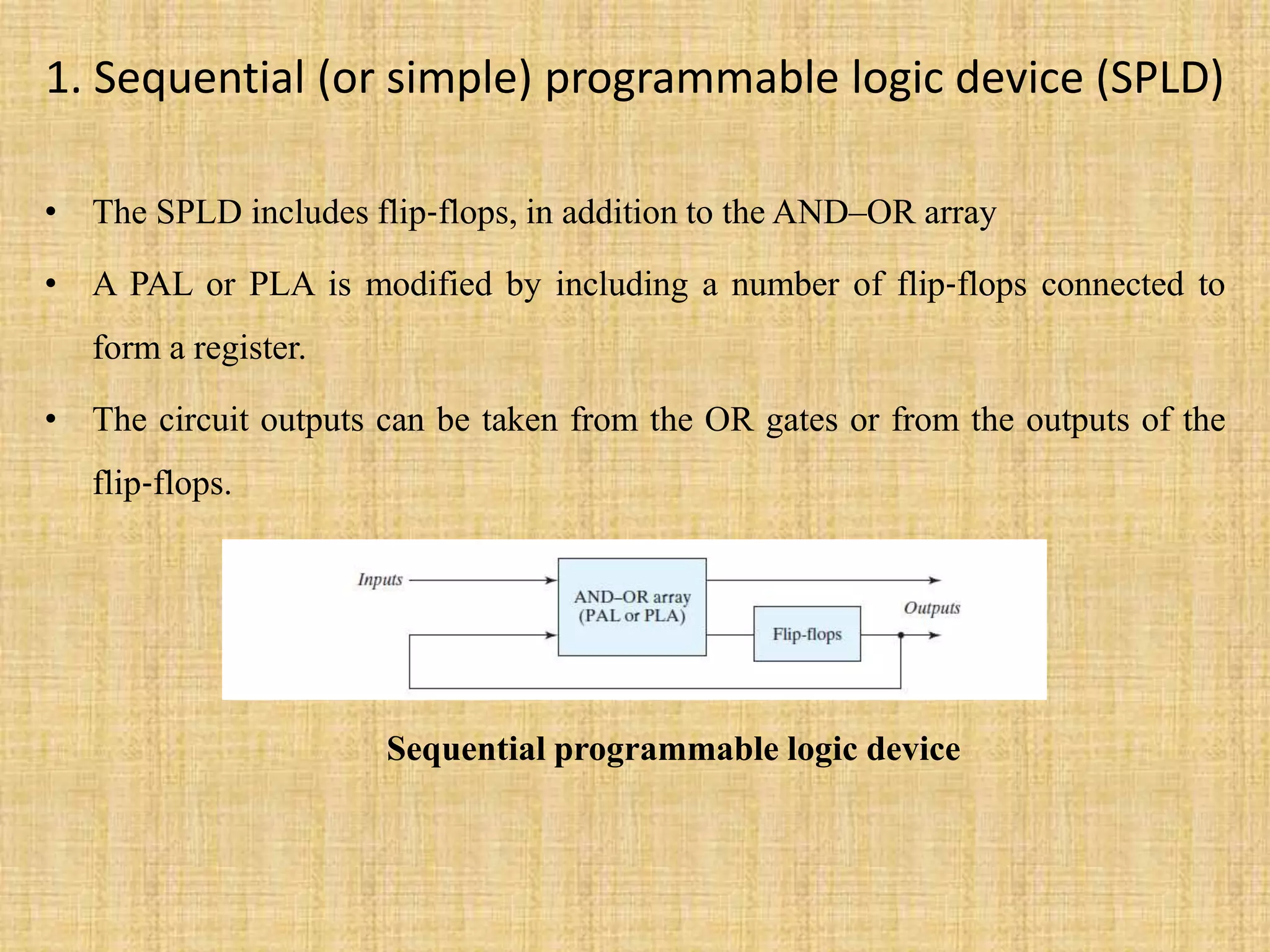
Digital Electronics
UNIT V PROGRAMMABLE LOGIC
DEVICES
R.Kanmani
Assistant Professor (Sr.Gr)/ECE
Sri Ramakrishna Institute of Technology
Coimbatore.
Memory Unit
• A memory unit is a device to which binary information is stored and
retrieved when needed
• Eg. 1 KB of memory  2^10= 1024
 2^k =1024, Hence k=10
 k address lines=1024 address lines
 Each 1024 locations has 8 bit Data(Byte)
• Example – 1024x16 memory Content
Memory operation
Write and Read Operations
Write Operation
1. Apply the binary address of the
desired word to the address lines.
2. Apply the data bits that must be
stored in memory to the data input
lines.
3. Activate the write input.
Read Operation
• 1. Apply the binary address of the
desired word to the address lines.
• 2. Activate the read input.
Classification of Memories
• Memory
ROM RAM
Masked ROM PROM EPROM EEPROM
Static
RAM
Dynamic
RAM
Random Access Memory (RAM)
 Can be written to or read from.
 Read/Write memory
 Reading from RAM is non-destructive.
 Access time to read from any memory location is the same.
 As compared to serial access memory.
 Volatile
 Information is lost when power is removed.
Random Access Memory (RAM)
 Static Random Access Memory (SRAM)
 Based on the Flip-Flop
 Requires a large number of transistors
 Fast
 Dynamic Random Access Memory (DRAM)
 Uses a single transistor to store charge
 Requires very few transistors
 Must be periodically refreshed
 Slow(er)
SRAM- Memory Cell
Internal Construction -SRAM Block Diagram
Construction of 4x4 RAM
Coincident Decoding
• For 1K-word memory instead of using 10 x1024 decoder, we use two 5x32
decoder in a two dimensional selection scheme.
• A 10x1024 decoder requires 1024 AND gates with 10 inputs each, whereas
when we use two 5x32 decoder it requires totally 64 AND gates with five
inputs each
• 10 Bit address is split into MSB 5 bits and LSB 5 bits. The MSB bits are
given to X and LSB bits are given to y
Coincident Decoding-Example
Two-dimensional decoding structure for a 1K-word memory
DRAM
• SRAM typically has 6 transistors
• DRAM consists of only one transistor and capacitor
• Capacitor charge will be discharged with respect to time. Hence it should
be periodically recharged.
• DRAMS have 4 times the density and cost is also 4 times less
Address multiplexing for 64K DRAM
Random Access Memory
Read Cycle
Random Access Memory
Write Cycle
Read Only Memory (ROM)
 Can only be read from.
 Memory is written (or “programmed”) once
 Reading from ROM is non-destructive.
 Access time to read from any memory location is the same.
 As compared to serial access memory.
 Non-Volatile
 Information is retained even after power is removed.
Read Only Memory
• The inputs provide the address for memory, and the outputs give the data
bits of the stored word that is selected by the address.
• The number of words in a ROM is determined from the fact that k address
input lines are needed to specify 2k words.
• Note that ROM does not have data inputs, because it does not have a write
operation.
Eg:32x 8 ROM
• Here 2^k = 32 and n=8, Therefore 32 address locations and 8 output lines.
The 32 addresses are generated by a 5 x32 decoder.
Internal logic of a 32x8 ROM
Programming ROM
ROM Example
• Design a combinational circuit using a ROM. The circuit accepts a three‐bit
number and outputs a binary number equal to the square of the input
number.
Types of Read Only Memory (ROM)
 Programmable Read Only Memory (PROM)
 Can be “programmed”
 Erasable PROM (EPROM)
 Can be “programmed” and erased
 Electrically Erasable PROM (EEPROM)
 Can be erased using an electrical signal
 UV Erasable PROM (UVEPROM)
 Can be erased using Ultraviolet light
Combinational PLDs
• The PROM is a combinational programmable logic device (PLD)—an
integrated circuit with programmable gates divided into an AND array and
an OR array to provide an AND–OR sum‐of‐product implementation.
• Three types
a) PROM (Programmable read only memory)
b) PAL (Programmable Array logic)
c) PLA (Programmable Logic Array)
Types of Combinational PLDs
1.Programmable Read Only Memory(PROM)
2.Programmable Array Logic(PAL)
3.Programmbale Logic Array (PLA)
Programmable Logic Array(PLA)
• The PLA is similar in concept to the PROM, except that the PLA does not
provide full decoding of the variables and does not generate all the
minterms.
• The decoder is replaced by an array of AND gates that can be programmed
to generate any product term of the input variables.
• The product terms are then connected to OR gates to provide the sum of
products for the required Boolean functions.
Boolean Function Implementation in PLA
• Eg. Implement the following fn in PLA
PLA with three inputs, four product terms and two outputs
• PLA Programming Table
Boolean Function Implementation in PLA
(Contd.)
PLA Example
• Implement the following two Boolean functions with a PLA:
Programmable Array Logic(PAL)
• The PAL is a programmable logic device with a fixed OR
array and a programmable AND array. Because only the AND
gates are programmable, the PAL is easier to program than, but
is not as flexible as, the PLA.
PAL with four inputs, four outputs and a three-wide AND-OR structure
PAL Implementation Example
• Implement the function
• After K-map simplification
w = ABC’+A’B’CD’
x = A+BCD
y = A’B+CD+B’D’
z = ABC’+A’B’CD’+AC’D’+A’B’C’D
• z can be written in terms of w as
z= w+ AC’D’+A’B’C’D
PAL Implementation Example(Contd.)
w = ABC’+A’B’CD’
x = A+BCD
y = A’B+CD+B’D’
z = w+ AC’D’+A’B’C’D
PAL Programming table
Sequential Programmable Devices
• Digital systems are designed with flip‐flops and gates. Since the
combinational PLD consists of only gates, it is necessary to include
external flip‐flops when they are used in the design.
• Sequential programmable devices include both gates and flip‐flops. In this
way, the device can be programmed to perform a variety of
sequential‐circuit functions.
• Three types
1. Sequential (or simple) programmable logic device (SPLD)
2. Complex programmable logic device (CPLD)
3. Field‐programmable gate array (FPGA)
1. Sequential (or simple) programmable logic device (SPLD)
• The SPLD includes flip‐flops, in addition to the AND–OR array
• A PAL or PLA is modified by including a number of flip‐flops connected to
form a register.
• The circuit outputs can be taken from the OR gates or from the outputs of the
flip‐flops.
Sequential programmable logic device
CPLD
• CPLD-The device consists of multiple PLDs interconnected through a
programmable switch matrix.
• The input–output (I/O) blocks provide the connections to the IC pins. Each I/O pin
is driven by a three state buffer and can be programmed to act as input or output.
• The switch matrix receives inputs from the I/O block and directs them to the
individual macrocells.
• Similarly, selected outputs from macrocells are sent to the outputs as needed.
• Each PLD typically contains from 8 to 16 macrocells, usually fully connected.
• If a macrocell has unused product terms, they can be used by other nearby
macrocells. In some cases the macrocell flip‐flop is programmed to act as a D, JK,
or T flip‐flop.
CPLD
General CPLD configuration

Unit v memory & programmable logic devices

  • 1.
    Digital Electronics UNIT VPROGRAMMABLE LOGIC DEVICES R.Kanmani Assistant Professor (Sr.Gr)/ECE Sri Ramakrishna Institute of Technology Coimbatore.
  • 2.
    Memory Unit • Amemory unit is a device to which binary information is stored and retrieved when needed • Eg. 1 KB of memory  2^10= 1024  2^k =1024, Hence k=10  k address lines=1024 address lines  Each 1024 locations has 8 bit Data(Byte)
  • 3.
    • Example –1024x16 memory Content
  • 4.
  • 5.
    Write and ReadOperations Write Operation 1. Apply the binary address of the desired word to the address lines. 2. Apply the data bits that must be stored in memory to the data input lines. 3. Activate the write input. Read Operation • 1. Apply the binary address of the desired word to the address lines. • 2. Activate the read input.
  • 6.
    Classification of Memories •Memory ROM RAM Masked ROM PROM EPROM EEPROM Static RAM Dynamic RAM
  • 7.
    Random Access Memory(RAM)  Can be written to or read from.  Read/Write memory  Reading from RAM is non-destructive.  Access time to read from any memory location is the same.  As compared to serial access memory.  Volatile  Information is lost when power is removed.
  • 8.
    Random Access Memory(RAM)  Static Random Access Memory (SRAM)  Based on the Flip-Flop  Requires a large number of transistors  Fast  Dynamic Random Access Memory (DRAM)  Uses a single transistor to store charge  Requires very few transistors  Must be periodically refreshed  Slow(er)
  • 9.
    SRAM- Memory Cell InternalConstruction -SRAM Block Diagram
  • 10.
  • 11.
    Coincident Decoding • For1K-word memory instead of using 10 x1024 decoder, we use two 5x32 decoder in a two dimensional selection scheme. • A 10x1024 decoder requires 1024 AND gates with 10 inputs each, whereas when we use two 5x32 decoder it requires totally 64 AND gates with five inputs each • 10 Bit address is split into MSB 5 bits and LSB 5 bits. The MSB bits are given to X and LSB bits are given to y
  • 12.
  • 13.
    DRAM • SRAM typicallyhas 6 transistors • DRAM consists of only one transistor and capacitor • Capacitor charge will be discharged with respect to time. Hence it should be periodically recharged. • DRAMS have 4 times the density and cost is also 4 times less
  • 14.
  • 15.
  • 16.
  • 17.
    Read Only Memory(ROM)  Can only be read from.  Memory is written (or “programmed”) once  Reading from ROM is non-destructive.  Access time to read from any memory location is the same.  As compared to serial access memory.  Non-Volatile  Information is retained even after power is removed.
  • 18.
    Read Only Memory •The inputs provide the address for memory, and the outputs give the data bits of the stored word that is selected by the address. • The number of words in a ROM is determined from the fact that k address input lines are needed to specify 2k words. • Note that ROM does not have data inputs, because it does not have a write operation.
  • 19.
    Eg:32x 8 ROM •Here 2^k = 32 and n=8, Therefore 32 address locations and 8 output lines. The 32 addresses are generated by a 5 x32 decoder. Internal logic of a 32x8 ROM
  • 20.
  • 21.
    ROM Example • Designa combinational circuit using a ROM. The circuit accepts a three‐bit number and outputs a binary number equal to the square of the input number.
  • 22.
    Types of ReadOnly Memory (ROM)  Programmable Read Only Memory (PROM)  Can be “programmed”  Erasable PROM (EPROM)  Can be “programmed” and erased  Electrically Erasable PROM (EEPROM)  Can be erased using an electrical signal  UV Erasable PROM (UVEPROM)  Can be erased using Ultraviolet light
  • 23.
    Combinational PLDs • ThePROM is a combinational programmable logic device (PLD)—an integrated circuit with programmable gates divided into an AND array and an OR array to provide an AND–OR sum‐of‐product implementation. • Three types a) PROM (Programmable read only memory) b) PAL (Programmable Array logic) c) PLA (Programmable Logic Array)
  • 24.
    Types of CombinationalPLDs 1.Programmable Read Only Memory(PROM) 2.Programmable Array Logic(PAL) 3.Programmbale Logic Array (PLA)
  • 25.
    Programmable Logic Array(PLA) •The PLA is similar in concept to the PROM, except that the PLA does not provide full decoding of the variables and does not generate all the minterms. • The decoder is replaced by an array of AND gates that can be programmed to generate any product term of the input variables. • The product terms are then connected to OR gates to provide the sum of products for the required Boolean functions.
  • 26.
    Boolean Function Implementationin PLA • Eg. Implement the following fn in PLA PLA with three inputs, four product terms and two outputs
  • 27.
    • PLA ProgrammingTable Boolean Function Implementation in PLA (Contd.)
  • 28.
    PLA Example • Implementthe following two Boolean functions with a PLA:
  • 29.
    Programmable Array Logic(PAL) •The PAL is a programmable logic device with a fixed OR array and a programmable AND array. Because only the AND gates are programmable, the PAL is easier to program than, but is not as flexible as, the PLA.
  • 30.
    PAL with fourinputs, four outputs and a three-wide AND-OR structure
  • 31.
    PAL Implementation Example •Implement the function • After K-map simplification w = ABC’+A’B’CD’ x = A+BCD y = A’B+CD+B’D’ z = ABC’+A’B’CD’+AC’D’+A’B’C’D • z can be written in terms of w as z= w+ AC’D’+A’B’C’D
  • 32.
    PAL Implementation Example(Contd.) w= ABC’+A’B’CD’ x = A+BCD y = A’B+CD+B’D’ z = w+ AC’D’+A’B’C’D PAL Programming table
  • 34.
    Sequential Programmable Devices •Digital systems are designed with flip‐flops and gates. Since the combinational PLD consists of only gates, it is necessary to include external flip‐flops when they are used in the design. • Sequential programmable devices include both gates and flip‐flops. In this way, the device can be programmed to perform a variety of sequential‐circuit functions. • Three types 1. Sequential (or simple) programmable logic device (SPLD) 2. Complex programmable logic device (CPLD) 3. Field‐programmable gate array (FPGA)
  • 35.
    1. Sequential (orsimple) programmable logic device (SPLD) • The SPLD includes flip‐flops, in addition to the AND–OR array • A PAL or PLA is modified by including a number of flip‐flops connected to form a register. • The circuit outputs can be taken from the OR gates or from the outputs of the flip‐flops. Sequential programmable logic device
  • 36.
    CPLD • CPLD-The deviceconsists of multiple PLDs interconnected through a programmable switch matrix. • The input–output (I/O) blocks provide the connections to the IC pins. Each I/O pin is driven by a three state buffer and can be programmed to act as input or output. • The switch matrix receives inputs from the I/O block and directs them to the individual macrocells. • Similarly, selected outputs from macrocells are sent to the outputs as needed. • Each PLD typically contains from 8 to 16 macrocells, usually fully connected. • If a macrocell has unused product terms, they can be used by other nearby macrocells. In some cases the macrocell flip‐flop is programmed to act as a D, JK, or T flip‐flop.
  • 37.