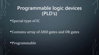
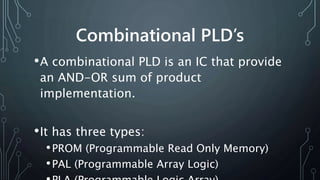
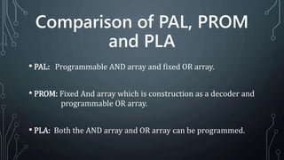
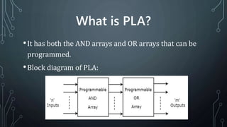
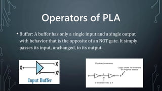
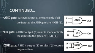
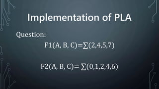
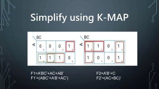
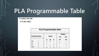
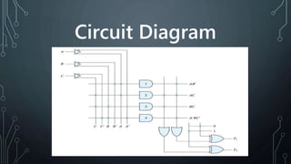
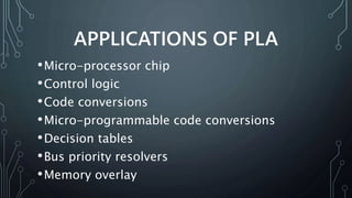
PROGRAMMABLE LOGIC
ARRAY (PLA)
DIGITAL LOGIC AND DESIGN
BSCS 2ND (MA)
GROUP 2
Programmable logic devices
(PLD’s)
•Special type of IC
•Contains array of AND gates and OR gates
•Programmable
Combinational PLD’s
•A combinational PLD is an IC that provide
an AND-OR sum of product
implementation.
•It has three types:
•PROM (Programmable Read Only Memory)
•PAL (Programmable Array Logic)
Comparison of PAL, PROM
and PLA
• PAL: Programmable AND array and fixed OR array.
• PROM: Fixed And array which is construction as a decoder and
programmable OR array.
• PLA: Both the AND array and OR array can be programmed.
What is PLA?
•It has both the AND arrays and OR arrays that can be
programmed.
•Block diagram of PLA:
Operators of PLA
• Buffer: A buffer has only a single input and a single output
with behavior that is the opposite of an NOT gate. It simply
passes its input, unchanged, to its output.
CONTINUED…
•AND gate: A HIGH output (1) results only if all
the input to the AND gate are HIGH (1).
•OR gate: A HIGH output (1) results if one or both
the inputs to the gate are HIGH (1).
•XOR gate: A HIGH output (1) results if (1) occurs
only one time.
Implementation of PLA
Question:
F1(A, B, C)=∑(2,4,5,7)
F2(A, B, C)= ∑(0,1,2,4,6)
Simplify using K-MAP
F1=A’BC’+AC+AB’ F2=A’B’+C
F1’=(ABC’+A’B’+AC’) F2’=(AC+BC)’
PLA Programmable Table
Circuit Diagram
ADVANTAGES OF PLA
•Less time consuming
•Easy to check and change
•Adaptive to new technology
DISADVANTAGES OF PLA
•Less speed
•Larger chip area
•Expensive
APPLICATIONS OF PLA
•Micro-processor chip
•Control logic
•Code conversions
•Micro-programmable code conversions
•Decision tables
•Bus priority resolvers
•Memory overlay
Questions
Programmable logic array (pla)

Programmable logic array (pla)