SlideShare a Scribd company logo
1 of 35
Download to read offline
Half Adder in Digital Logic
A half adder is a digital logic circuit that performs binary
addition of two single-bit binary numbers.
It has two inputs, A and B, and two outputs, SUM and CARRY.
The SUM output is the least significant bit (LSB) of the result,
while the CARRY output is the most significant bit (MSB) of
the result, indicating whether there was a carry-over from
the addition of the two inputs
Logical Expression:
For Sum:
Sum = A XOR B
For Carry:
Carry = A AND B
Implementation:
Advantages of Half Adder in Digital Logic :
1.Simplicity: A half viper is a straightforward circuit that requires a couple of fundamental
parts like XOR AND entryways. It is not difficult to carry out and can be utilized in
numerous advanced frameworks.
2.Speed: The half viper works at an extremely rapid, making it reasonable for use in fast
computerized circuits.
Disadvantages of Half Adder in Digital Logic :
1.Limited Usefulness: The half viper can add two single-piece numbers and produce a total
and a convey bit. It can’t perform expansion of multi-bit numbers, which requires the
utilization of additional intricate circuits like full adders.
2.Lack of Convey Info: The half snake doesn’t have a convey input, which restricts its value
in more mind boggling expansion tasks. A convey input is important to perform expansion
Application of Half Adder in Digital Logic:
1.Arithmetic circuits: Half adders are utilized in number-crunching circuits to add double
numbers. At the point when different half adders are associated in a chain, they can add
multi-bit double numbers.
2.Data handling: Half adders are utilized in information handling applications like
computerized signal handling, information encryption, and blunder adjustment.
3.Address unraveling: In memory tending to, half adders are utilized in address deciphering
circuits to produce the location of a particular memory area.
4.Encoder and decoder circuits: Half adders are utilized in encoder and decoder circuits for
computerized correspondence frameworks.
5.Multiplexers and demultiplexers: Half adders are utilized in multiplexers and
demultiplexers to choose and course information.
Full Adder
Full Adder is the adder that adds three inputs and produces two
outputs.
The first two inputs are A and B and the third input is an input carry
as C-IN.
The output carry is designated as C-OUT and the normal output is
designated as S which is SUM.
Characteristic Equations of Full Adder
Sum,S=A⊕B⊕Cin=A′B′Cin+A′BC′in+AB′C′in+ABCin
Carry,C=AB+ACin+BCin
Applications of Full Adder
Full adders are used in ALUs (arithmetic logic units) of CPUs of computers.
Full adders are used in calculators.
Full adders also help in carrying out multiplication of binary numbers.
Full adders are also used to realize critic digital circuits like multiplexers.
Full adders are used to generate memory addresses.
Half Subtractor
The half-subtractor is a combinational circuit which is used to perform subtraction of
two bits.
It has two inputs, A (minuend) and B (subtrahend) and two outputs Difference and
Borrow.
Difference = A ⊕B
Borrow = A' B
Full Subtractor
A full subtractor is a combinational circuit that performs
subtraction involving three bits, namely A (minuend), B
(subtrahend), and Bin (borrow-in) .
It accepts three inputs: A (minuend), B (subtrahend) and a Bin
(borrow bit) and it produces two outputs: D (difference) and
Bout (borrow out).
D = A ⊕B ⊕Bin
Bout = A' Bin + A'
B + B Bin
Programmable Logic Device?
integrated circuit that contains an array of logic elements and
interconnections that can be programmed by the user to
implement a desired logic function.
The logic elements are usually simple combinational or sequential
circuits, such as AND, OR, NOT, and XOR gates, or registers.
The interconnections are usually programmable switches or
multiplexers that can connect the inputs and outputs of the logic
elements in different ways.
The programming of a PLD can be done using a hardware description language
(HDL), such as Verilog or VHDL, or a graphical user interface (GUI) software tool.
The programming code or file is then downloaded to the PLD using a special device
programmer or a standard interface, such as JTAG or USB.
The programming code or file determines how the logic elements and
interconnections are configured to perform the desired logic functio
Types of Programmable Logic Devices
Programmable Read-Only Memory (PROM):
Programmable Logic Array (PLA):
Programmable Array Logic (PAL):
Generic Array Logic (GAL): This is a device that consists of a
programmable array of AND gates and a fixed array of OR gates that can
implement any sum-of-products logic expression.
The AND array is programmed by using electrically erasable
programmable read-only memory (EEPROM) cells in the rows that
connect the inputs to the AND gates.
The OR array is fixed and has a predefined number of outputs. The
advantage of GALs over PALs is that they can be erased and
reprogrammed electrically.
Applications and Advantages of Programmable Logic Devices
Digital Systems Design: PLDs are used to design digital systems such
as microprocessors, microcontrollers, digital signal processors,
embedded systems, computer peripherals, communication devices,
etc.
PLDs offer flexibility in designing complex logic functions with fewer
hardware components and wiring than discrete logic devices.
Rapid Prototyping: PLDs are used to prototype digital systems
quickly and easily without requiring expensive fabrication processes
or long development cycles.
PLDs allow the testing and debugging of digital systems on-the-fly
by modifying their programming code without affecting their
physical structure.
Performance: PLDs offer high performance in terms of speed, power
consumption, reliability, and scalability than fixed logic devices. PLDs
enable parallel processing by allowing multiple operations to be
performed simultaneously using different parts of the device.
Programmable Read Only Memory PROM
Read Only Memory ROM is a memory device, which stores the binary
information permanently. That means, we can’t change that stored
information by any means later.
If the ROM has programmable feature, then it is called as Programmable
ROM PROM The user has the flexibility to program the binary information
electrically once by using PROM programmer.
Here, the inputs of AND gates are not of programmable type.
So, we have to generate 2n product terms by using 2 ^n AND gates
having n inputs each. We can implement these product terms by using
nx2^n decoder. So, this decoder generates ‘n’ min terms.
Here, the inputs of OR gates are programmable. That means, we can
program any number of required product terms, since all the outputs
of AND gates are applied as inputs to each OR gate. Therefore, the
outputs of PROM will be in the form of sum of min terms.
Let us implement the following Boolean functions using PROM.
A(X,Y,Z)=∑m(5,6,7)
B(X,Y,Z)=∑m(3,5,6,7)
Programmable Array Logic PAL
PAL is a programmable logic device that has Programmable AND array
& fixed OR array.
The advantage of PAL is that we can generate only the required
product terms of Boolean function instead of generating all the min
terms by using programmable AND gates.
Let us implement the following Boolean functions using PAL.
A=XY+XZ′
A=XY′+YZ′
The programmable AND gates have the access of both normal and
complemented inputs of variables. In the above figure, the inputs
X, X′
, Y, Y′
, Z & Z′
, are available at the inputs of each AND gate.
So, program only the required literals in order to generate one product
term by each AND gate. The symbol ‘X’ is used for programmable
connections.
Here, the inputs of OR gates are of fixed type. So, the necessary product
terms are connected to inputs of each OR gate. So that the OR gates
produce the respective Boolean functions. The symbol ‘.’ is used for fixed
connections.
Programmable Logic Array PLA
PLA is a programmable logic device that has both Programmable AND
array & Programmable OR array. Hence, it is the most flexible PLD.
Let us implement the following Boolean functions using PLA.
A=XY+XZ′
B=XY′+YZ+XZ′
The given two functions are in sum of products form. The number of
product terms present in the given Boolean functions A & B are two and
three respectively. One product term, Z′X
is common in each function.
So, we require four programmable AND gates & two programmable OR
gates for producing those two functions
siudhai ki marks sheih shuuu kvms jiiiiv

More Related Content

Similar to siudhai ki marks sheih shuuu kvms jiiiiv

High speed customized serial protocol for IP integration on FPGA based SOC ap...
High speed customized serial protocol for IP integration on FPGA based SOC ap...High speed customized serial protocol for IP integration on FPGA based SOC ap...
High speed customized serial protocol for IP integration on FPGA based SOC ap...IJMER
 
Nt1310 Unit 5 Algorithm
Nt1310 Unit 5 AlgorithmNt1310 Unit 5 Algorithm
Nt1310 Unit 5 AlgorithmAngie Lee
 
Introduction to FPGA, VHDL
Introduction to FPGA, VHDL  Introduction to FPGA, VHDL
Introduction to FPGA, VHDL Amr Rashed
 
System design using HDL - Module 3
System design using HDL - Module 3System design using HDL - Module 3
System design using HDL - Module 3Aravinda Koithyar
 
arduinocourse-180308074529 (1).pdf
arduinocourse-180308074529 (1).pdfarduinocourse-180308074529 (1).pdf
arduinocourse-180308074529 (1).pdfssusere5db05
 
Microcontroller
MicrocontrollerMicrocontroller
MicrocontrollerSpitiq
 
IRJET - Wireless Transmission of Data using LDPC Codes based on Raspberry Pi
IRJET - Wireless Transmission of Data using LDPC Codes based on Raspberry PiIRJET - Wireless Transmission of Data using LDPC Codes based on Raspberry Pi
IRJET - Wireless Transmission of Data using LDPC Codes based on Raspberry PiIRJET Journal
 
UNIT I- CPLD & FPGA ARCHITECTURE & APPLICATIONS
UNIT I- CPLD & FPGA ARCHITECTURE & APPLICATIONSUNIT I- CPLD & FPGA ARCHITECTURE & APPLICATIONS
UNIT I- CPLD & FPGA ARCHITECTURE & APPLICATIONSDr.YNM
 
Introduction to uP-Chadasdffpter I-3.ppt
Introduction to uP-Chadasdffpter I-3.pptIntroduction to uP-Chadasdffpter I-3.ppt
Introduction to uP-Chadasdffpter I-3.pptYAGYABAHADURSHAHI
 
Introduction to computer architecture .pptx
Introduction to computer architecture .pptxIntroduction to computer architecture .pptx
Introduction to computer architecture .pptxFatma Sayed Ibrahim
 
Lecture 10.cont,11 (plc)
Lecture 10.cont,11 (plc)Lecture 10.cont,11 (plc)
Lecture 10.cont,11 (plc)Mohamed Atef
 
FPGA implementation of synchronous and asynchronous counter and simulation of...
FPGA implementation of synchronous and asynchronous counter and simulation of...FPGA implementation of synchronous and asynchronous counter and simulation of...
FPGA implementation of synchronous and asynchronous counter and simulation of...ASHIMA GUPTA
 
Design and Implementation of Low Power High Speed Symmetric Decoder Structure...
Design and Implementation of Low Power High Speed Symmetric Decoder Structure...Design and Implementation of Low Power High Speed Symmetric Decoder Structure...
Design and Implementation of Low Power High Speed Symmetric Decoder Structure...Dr. Amarjeet Singh
 

Similar to siudhai ki marks sheih shuuu kvms jiiiiv (20)

EEE226a.ppt
EEE226a.pptEEE226a.ppt
EEE226a.ppt
 
High speed customized serial protocol for IP integration on FPGA based SOC ap...
High speed customized serial protocol for IP integration on FPGA based SOC ap...High speed customized serial protocol for IP integration on FPGA based SOC ap...
High speed customized serial protocol for IP integration on FPGA based SOC ap...
 
Assignment
AssignmentAssignment
Assignment
 
Nt1310 Unit 5 Algorithm
Nt1310 Unit 5 AlgorithmNt1310 Unit 5 Algorithm
Nt1310 Unit 5 Algorithm
 
Introduction to FPGA, VHDL
Introduction to FPGA, VHDL  Introduction to FPGA, VHDL
Introduction to FPGA, VHDL
 
System design using HDL - Module 3
System design using HDL - Module 3System design using HDL - Module 3
System design using HDL - Module 3
 
Arduino course
Arduino courseArduino course
Arduino course
 
arduinocourse-180308074529 (1).pdf
arduinocourse-180308074529 (1).pdfarduinocourse-180308074529 (1).pdf
arduinocourse-180308074529 (1).pdf
 
Microcontroller
MicrocontrollerMicrocontroller
Microcontroller
 
Bus interface 8086
Bus interface 8086Bus interface 8086
Bus interface 8086
 
IRJET - Wireless Transmission of Data using LDPC Codes based on Raspberry Pi
IRJET - Wireless Transmission of Data using LDPC Codes based on Raspberry PiIRJET - Wireless Transmission of Data using LDPC Codes based on Raspberry Pi
IRJET - Wireless Transmission of Data using LDPC Codes based on Raspberry Pi
 
UNIT I- CPLD & FPGA ARCHITECTURE & APPLICATIONS
UNIT I- CPLD & FPGA ARCHITECTURE & APPLICATIONSUNIT I- CPLD & FPGA ARCHITECTURE & APPLICATIONS
UNIT I- CPLD & FPGA ARCHITECTURE & APPLICATIONS
 
Development of plc
Development of plcDevelopment of plc
Development of plc
 
ppt.pptx
ppt.pptxppt.pptx
ppt.pptx
 
Introduction to uP-Chadasdffpter I-3.ppt
Introduction to uP-Chadasdffpter I-3.pptIntroduction to uP-Chadasdffpter I-3.ppt
Introduction to uP-Chadasdffpter I-3.ppt
 
Introduction to computer architecture .pptx
Introduction to computer architecture .pptxIntroduction to computer architecture .pptx
Introduction to computer architecture .pptx
 
Lecture 10.cont,11 (plc)
Lecture 10.cont,11 (plc)Lecture 10.cont,11 (plc)
Lecture 10.cont,11 (plc)
 
FPGA implementation of synchronous and asynchronous counter and simulation of...
FPGA implementation of synchronous and asynchronous counter and simulation of...FPGA implementation of synchronous and asynchronous counter and simulation of...
FPGA implementation of synchronous and asynchronous counter and simulation of...
 
מצגת פרויקט
מצגת פרויקטמצגת פרויקט
מצגת פרויקט
 
Design and Implementation of Low Power High Speed Symmetric Decoder Structure...
Design and Implementation of Low Power High Speed Symmetric Decoder Structure...Design and Implementation of Low Power High Speed Symmetric Decoder Structure...
Design and Implementation of Low Power High Speed Symmetric Decoder Structure...
 

Recently uploaded

Mobile Application Development-Android and It’s Tools
Mobile Application Development-Android and It’s ToolsMobile Application Development-Android and It’s Tools
Mobile Application Development-Android and It’s ToolsChandrakantDivate1
 
Mobile App Penetration Testing Bsides312
Mobile App Penetration Testing Bsides312Mobile App Penetration Testing Bsides312
Mobile App Penetration Testing Bsides312wphillips114
 
Bromazolam CAS 71368-80-4 high quality opiates, Safe transportation, 99% pure
Bromazolam CAS 71368-80-4 high quality opiates, Safe transportation, 99% pureBromazolam CAS 71368-80-4 high quality opiates, Safe transportation, 99% pure
Bromazolam CAS 71368-80-4 high quality opiates, Safe transportation, 99% pureamy56318795
 
Abortion pills in Riyadh+966572737505 cytotec jeddah
Abortion pills in Riyadh+966572737505 cytotec jeddahAbortion pills in Riyadh+966572737505 cytotec jeddah
Abortion pills in Riyadh+966572737505 cytotec jeddahsamsungultra782445
 
Mobile Application Development-Components and Layouts
Mobile Application Development-Components and LayoutsMobile Application Development-Components and Layouts
Mobile Application Development-Components and LayoutsChandrakantDivate1
 
原版定制英国伦敦大学金史密斯学院毕业证原件一模一样
原版定制英国伦敦大学金史密斯学院毕业证原件一模一样原版定制英国伦敦大学金史密斯学院毕业证原件一模一样
原版定制英国伦敦大学金史密斯学院毕业证原件一模一样AS
 
Android Application Components with Implementation & Examples
Android Application Components with Implementation & ExamplesAndroid Application Components with Implementation & Examples
Android Application Components with Implementation & ExamplesChandrakantDivate1
 
Mobile Application Development- Configuration and Android Installation
Mobile Application Development- Configuration and Android InstallationMobile Application Development- Configuration and Android Installation
Mobile Application Development- Configuration and Android InstallationChandrakantDivate1
 

Recently uploaded (9)

Mobile Application Development-Android and It’s Tools
Mobile Application Development-Android and It’s ToolsMobile Application Development-Android and It’s Tools
Mobile Application Development-Android and It’s Tools
 
Mobile App Penetration Testing Bsides312
Mobile App Penetration Testing Bsides312Mobile App Penetration Testing Bsides312
Mobile App Penetration Testing Bsides312
 
Bromazolam CAS 71368-80-4 high quality opiates, Safe transportation, 99% pure
Bromazolam CAS 71368-80-4 high quality opiates, Safe transportation, 99% pureBromazolam CAS 71368-80-4 high quality opiates, Safe transportation, 99% pure
Bromazolam CAS 71368-80-4 high quality opiates, Safe transportation, 99% pure
 
Abortion pills in Riyadh+966572737505 cytotec jeddah
Abortion pills in Riyadh+966572737505 cytotec jeddahAbortion pills in Riyadh+966572737505 cytotec jeddah
Abortion pills in Riyadh+966572737505 cytotec jeddah
 
Mobile Application Development-Components and Layouts
Mobile Application Development-Components and LayoutsMobile Application Development-Components and Layouts
Mobile Application Development-Components and Layouts
 
原版定制英国伦敦大学金史密斯学院毕业证原件一模一样
原版定制英国伦敦大学金史密斯学院毕业证原件一模一样原版定制英国伦敦大学金史密斯学院毕业证原件一模一样
原版定制英国伦敦大学金史密斯学院毕业证原件一模一样
 
Android Application Components with Implementation & Examples
Android Application Components with Implementation & ExamplesAndroid Application Components with Implementation & Examples
Android Application Components with Implementation & Examples
 
Mobile Application Development- Configuration and Android Installation
Mobile Application Development- Configuration and Android InstallationMobile Application Development- Configuration and Android Installation
Mobile Application Development- Configuration and Android Installation
 
Obat Penggugur Kandungan Di Apotik Kimia Farma (087776558899)
Obat Penggugur Kandungan Di Apotik Kimia Farma (087776558899)Obat Penggugur Kandungan Di Apotik Kimia Farma (087776558899)
Obat Penggugur Kandungan Di Apotik Kimia Farma (087776558899)
 

siudhai ki marks sheih shuuu kvms jiiiiv

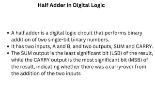
  • 1. Half Adder in Digital Logic A half adder is a digital logic circuit that performs binary addition of two single-bit binary numbers. It has two inputs, A and B, and two outputs, SUM and CARRY. The SUM output is the least significant bit (LSB) of the result, while the CARRY output is the most significant bit (MSB) of the result, indicating whether there was a carry-over from the addition of the two inputs
  • 5. Advantages of Half Adder in Digital Logic : 1.Simplicity: A half viper is a straightforward circuit that requires a couple of fundamental parts like XOR AND entryways. It is not difficult to carry out and can be utilized in numerous advanced frameworks. 2.Speed: The half viper works at an extremely rapid, making it reasonable for use in fast computerized circuits. Disadvantages of Half Adder in Digital Logic : 1.Limited Usefulness: The half viper can add two single-piece numbers and produce a total and a convey bit. It can’t perform expansion of multi-bit numbers, which requires the utilization of additional intricate circuits like full adders. 2.Lack of Convey Info: The half snake doesn’t have a convey input, which restricts its value in more mind boggling expansion tasks. A convey input is important to perform expansion
  • 6. Application of Half Adder in Digital Logic: 1.Arithmetic circuits: Half adders are utilized in number-crunching circuits to add double numbers. At the point when different half adders are associated in a chain, they can add multi-bit double numbers. 2.Data handling: Half adders are utilized in information handling applications like computerized signal handling, information encryption, and blunder adjustment. 3.Address unraveling: In memory tending to, half adders are utilized in address deciphering circuits to produce the location of a particular memory area. 4.Encoder and decoder circuits: Half adders are utilized in encoder and decoder circuits for computerized correspondence frameworks. 5.Multiplexers and demultiplexers: Half adders are utilized in multiplexers and demultiplexers to choose and course information.
  • 7. Full Adder Full Adder is the adder that adds three inputs and produces two outputs. The first two inputs are A and B and the third input is an input carry as C-IN. The output carry is designated as C-OUT and the normal output is designated as S which is SUM.
  • 8.
  • 9.
  • 10.
  • 11. Characteristic Equations of Full Adder Sum,S=A⊕B⊕Cin=A′B′Cin+A′BC′in+AB′C′in+ABCin Carry,C=AB+ACin+BCin
  • 12. Applications of Full Adder Full adders are used in ALUs (arithmetic logic units) of CPUs of computers. Full adders are used in calculators. Full adders also help in carrying out multiplication of binary numbers. Full adders are also used to realize critic digital circuits like multiplexers. Full adders are used to generate memory addresses.
  • 13. Half Subtractor The half-subtractor is a combinational circuit which is used to perform subtraction of two bits. It has two inputs, A (minuend) and B (subtrahend) and two outputs Difference and Borrow.
  • 14. Difference = A ⊕B Borrow = A' B
  • 15.
  • 16. Full Subtractor A full subtractor is a combinational circuit that performs subtraction involving three bits, namely A (minuend), B (subtrahend), and Bin (borrow-in) . It accepts three inputs: A (minuend), B (subtrahend) and a Bin (borrow bit) and it produces two outputs: D (difference) and Bout (borrow out).
  • 17.
  • 18. D = A ⊕B ⊕Bin Bout = A' Bin + A' B + B Bin
  • 19.
  • 20. Programmable Logic Device? integrated circuit that contains an array of logic elements and interconnections that can be programmed by the user to implement a desired logic function. The logic elements are usually simple combinational or sequential circuits, such as AND, OR, NOT, and XOR gates, or registers. The interconnections are usually programmable switches or multiplexers that can connect the inputs and outputs of the logic elements in different ways.
  • 21. The programming of a PLD can be done using a hardware description language (HDL), such as Verilog or VHDL, or a graphical user interface (GUI) software tool. The programming code or file is then downloaded to the PLD using a special device programmer or a standard interface, such as JTAG or USB. The programming code or file determines how the logic elements and interconnections are configured to perform the desired logic functio
  • 22. Types of Programmable Logic Devices Programmable Read-Only Memory (PROM): Programmable Logic Array (PLA): Programmable Array Logic (PAL): Generic Array Logic (GAL): This is a device that consists of a programmable array of AND gates and a fixed array of OR gates that can implement any sum-of-products logic expression. The AND array is programmed by using electrically erasable programmable read-only memory (EEPROM) cells in the rows that connect the inputs to the AND gates. The OR array is fixed and has a predefined number of outputs. The advantage of GALs over PALs is that they can be erased and reprogrammed electrically.
  • 23. Applications and Advantages of Programmable Logic Devices Digital Systems Design: PLDs are used to design digital systems such as microprocessors, microcontrollers, digital signal processors, embedded systems, computer peripherals, communication devices, etc. PLDs offer flexibility in designing complex logic functions with fewer hardware components and wiring than discrete logic devices. Rapid Prototyping: PLDs are used to prototype digital systems quickly and easily without requiring expensive fabrication processes or long development cycles. PLDs allow the testing and debugging of digital systems on-the-fly by modifying their programming code without affecting their physical structure.
  • 24. Performance: PLDs offer high performance in terms of speed, power consumption, reliability, and scalability than fixed logic devices. PLDs enable parallel processing by allowing multiple operations to be performed simultaneously using different parts of the device.
  • 25. Programmable Read Only Memory PROM Read Only Memory ROM is a memory device, which stores the binary information permanently. That means, we can’t change that stored information by any means later. If the ROM has programmable feature, then it is called as Programmable ROM PROM The user has the flexibility to program the binary information electrically once by using PROM programmer.
  • 26.
  • 27. Here, the inputs of AND gates are not of programmable type. So, we have to generate 2n product terms by using 2 ^n AND gates having n inputs each. We can implement these product terms by using nx2^n decoder. So, this decoder generates ‘n’ min terms. Here, the inputs of OR gates are programmable. That means, we can program any number of required product terms, since all the outputs of AND gates are applied as inputs to each OR gate. Therefore, the outputs of PROM will be in the form of sum of min terms.
  • 28. Let us implement the following Boolean functions using PROM. A(X,Y,Z)=∑m(5,6,7) B(X,Y,Z)=∑m(3,5,6,7)
  • 29. Programmable Array Logic PAL PAL is a programmable logic device that has Programmable AND array & fixed OR array. The advantage of PAL is that we can generate only the required product terms of Boolean function instead of generating all the min terms by using programmable AND gates.
  • 30.
  • 31. Let us implement the following Boolean functions using PAL. A=XY+XZ′ A=XY′+YZ′
  • 32. The programmable AND gates have the access of both normal and complemented inputs of variables. In the above figure, the inputs X, X′ , Y, Y′ , Z & Z′ , are available at the inputs of each AND gate. So, program only the required literals in order to generate one product term by each AND gate. The symbol ‘X’ is used for programmable connections. Here, the inputs of OR gates are of fixed type. So, the necessary product terms are connected to inputs of each OR gate. So that the OR gates produce the respective Boolean functions. The symbol ‘.’ is used for fixed connections.
  • 33. Programmable Logic Array PLA PLA is a programmable logic device that has both Programmable AND array & Programmable OR array. Hence, it is the most flexible PLD.
  • 34. Let us implement the following Boolean functions using PLA. A=XY+XZ′ B=XY′+YZ+XZ′ The given two functions are in sum of products form. The number of product terms present in the given Boolean functions A & B are two and three respectively. One product term, Z′X is common in each function. So, we require four programmable AND gates & two programmable OR gates for producing those two functions