Downloaded 449 times
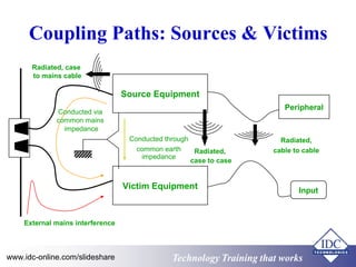
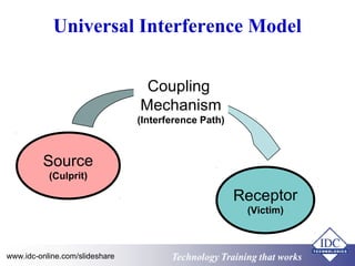
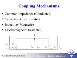
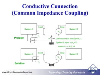
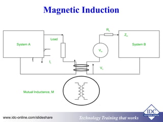
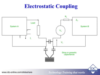
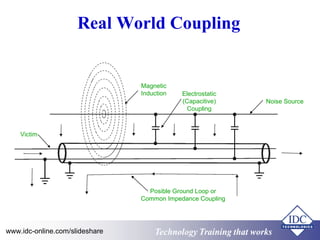
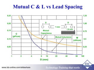
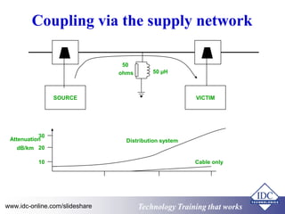
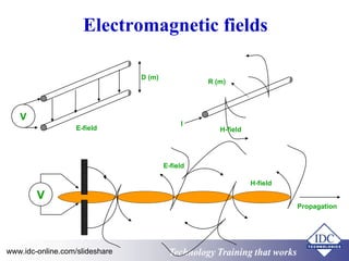
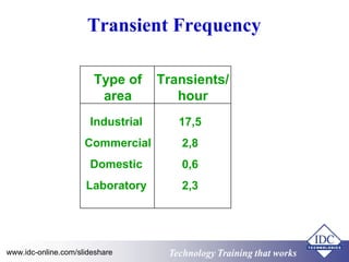
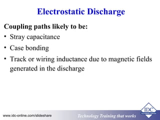
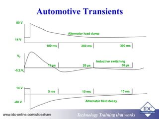
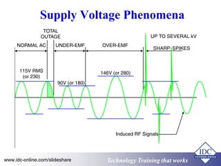


The document provides an overview of practical shielding, EMC/EMI, noise reduction, earthing, and circuit board layout technologies. It discusses sources of interference, coupling mechanisms, and potential solutions to mitigate noise in electronic systems. Various coupling paths, such as common impedance and electromagnetic interference, are explored alongside the impacts of different transient sources on electronic devices.


