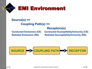
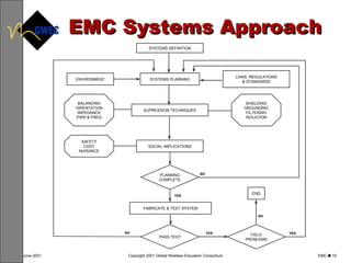
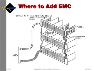
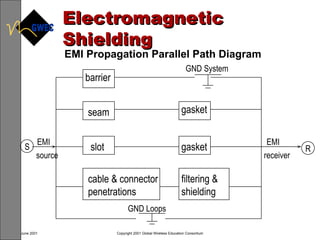
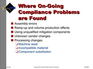
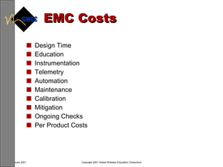
SlideShare a Scribd company logo
1 of 62
Introduction to Electromagnetic Compatibility (EMC)
EMC ,[object Object],[object Object],[object Object]
EMC ,[object Object],[object Object]
Table of Contents ,[object Object],[object Object],[object Object],[object Object],[object Object],[object Object],[object Object],[object Object],[object Object]
Overview ,[object Object],[object Object],[object Object],[object Object],[object Object]
Learning Objectives ,[object Object],[object Object],[object Object],[object Object],[object Object],After completing this module and all its activities, you will be able to:
EMC and the EMI Environment
Electromagnetic Compatibility ,[object Object]
Electromagnetic Compatibility (EMC) ,[object Object],[object Object],[object Object],[object Object],[object Object],[object Object]
Electromagnetic Interference (EMI) Environment
Exposure to Electromagnetic Frequencies Extra-low  frequency (ELF) Radio Microwave Infrared Visible light Ultra- violet X-rays,  gamma rays 1  Hz 10  Hz 100  Hz 1  kHz 10  kHz 100  kHz 1  MHz 10  MHz 100  MHz 1 GHz 10 GHz 100 GHz 10 12 Hz 10 13 Hz 10 14 Hz 10 15 Hz 10 16 Hz 10 17 Hz 10 18 Hz 10 20 Hz 10 19 Hz 10 21 Hz 10 22 Hz Frequency Nonionizing radiation Ionizing radiation Band Use Electric  power Video display terminals a AM Radio FM Radio, VHF TV Cellular Phones Microwave ovens, police radar,  satellite stations Heat  lamps Sun  lamps UHF TV Note: All of these frequencies designations are approximate because each category has fields over a range depending on the exact device.  a  Fields from video display terminals vary depending on the number of pictures per second on the screen: terminals also have 60 Hz fields.
Computer Emission Spectra COMPUTER SOURCE Hz  SPECTRUM CRT Anode  0  DC Electrostatic  (30 kV)  10 0 ULF (< 3 Hz) 10 1 AC Power  (50-60 Hz) 10 2 Vertical Scan  (5 Hz - 2 kHz) 10 3 ELF (3 Hz - 3 kHz) 10 4 VLF (3 kHz - 30 kHz) Horizontal Scan  (2 kHz - 400 kHz)  10 5 LF (30 kHz - 300 kHz) DC Power Supply  (400 Hz - 30 MHz)  10 6 MF (.3 MHz - 3 MHz) 10 7 HF (3 MHz - 30 MHz) Video Signal  (6 MHz)  10 8 VHF (30 MHz - 300 MHz) 10 9 UHF (300 MHz - 3 GHz) Digital Logic  (30 MHz - 40 GHz)  10 10 SHF (3 GHz - 30 GHz) 10 11 EHF (30 GHz - 300 GHz) 10 12 FAR-INFRARED 10 13 10 14 INFRARED CRT  10 15 VISIBLE LIGHT CRT 10 16 IONIZING RADIATION VDU CRT CPU
EMI Environment ,[object Object],Probable Annoyance Radiated Conducted SOURCE COUPLING PATHS VICTIM
Maximum Fields for Equipment Exposure Service Frequency Range (MHz) Effective Radiated Power (dBW) Usual Range of  Separation Distance Consequent Range of  Field Strengths (Volts per meter) LF Communications   0.014 - 0.5   54  5 - 20 km 0.25 - 1.0 & Navaids AM  Broadcast   0.5 - 1.6 47 - 50 0.5 - 2 km   0.2 -6.0 HF Amateur   1.8 - 3.0   30   20 - 100  m 3.0 - 15.0 HF Communications   1.5 - 3.0   40  4 - 20 km   0.001 - 0.25 General Radio   27 - 27.5   11   10 - 100  m   0.3 - 3.3 VHF Amateur   50 - 225 30 - 39   100 - 500  m 0.35 - 5.0 Communications  30 - 470 17 - 21   40 - 200  m   0.2 - 1.5 Fixed and Mobile TV - VHF   54 - 216 50 - 55 0.5 - 2 km 1.0 - 7.3  FM - Broadcast  86 - 106   50   0.25 - 1 km  2.0 - 8.3 TV - UHF   470 - 890   67 0.5 - 3 km 1.0 - 3.0 Radar   1,000 - 10, 000 90 - 97  2 - 20 km    0.1 - 90
Radiated Emission Data ,[object Object]
USA FCC Industrial, Scientific, and Medical (ISM) Equipment Emissions Unlimited Radiation Allowed on These Frequencies ISM Frequency Tolerance 6.78 MHz +   15.0  kHz 13.56 MHz +   7.0 kHz 27.12 MHz +  163.0  kHz 40.68 MHz +   20.0  KHz 915.00 MHz +   13.0  kHz 2,450.00 MHz +   50.0  MHz 5,800.00 MHz +   75.0 MHz 24,125.00 MHz +  125.0  MHz 61.25 GHz +  250.0 MHz 122.50 GHz +  500.0 MHz 245.00 GHz +   1.0  GHz Table 1 ISM Frequencies
EMI Environment ,[object Object],[object Object],[object Object],[object Object],[object Object],SOURCE COUPLING PATH RECEPTOR
EMC Design
EMC Systems Approach SYSTEMS DEFINITION ENVIRONMENT SYSTEMS PLANNING LAWS, REGULATIONS & STANDARDS SUPRESSION TECHNIQUES SOCIAL IMPLICATIONS PLANNING COMPLETE FABRICATE & TEST SYSTEM END BALANCING ORIENTATION IMPEDANCE PWR & FREQ SHIELDING GROUNDING FILTERING ISOLATION SAFETY COST NUISANCE FIELD PROBLEMS PASS TEST NO YES YES NO NO YES
The Design Guide ,[object Object],[object Object],[object Object],[object Object],[object Object],[object Object],[object Object],[object Object]
The Design Guide, cont. ,[object Object],[object Object],[object Object],[object Object],[object Object],[object Object],[object Object],[object Object]
Where to Add EMC
Differential Mode Radiated Emission Elevation Angle Amplitude Pattern
Common Mode Radiated Emissions
Typical Noise Path ,[object Object],[object Object],[object Object],[object Object],NOISE SOURCE COUPLING CHANNEL RECEPTOR
Parameters EMC PARAMETERS IN ELECTRONIC SYSTEM EMISSIONS IMMUNITY CROSSTALK THE IMPACT OF THE SYSTEM ON THE ENVIRONMENT THE ABILITY OF THE SYSTEM TO MEET SPECIFIED PERFORMANCE IN A SPECIFIED EMI ENVIRONMENT THE INTERACTION BETWEEN ANY PARTICULAR SYSTEMS
Electrostatic Discharge (ESD) EMI COUPLING TO ELECTRONIC INTERCONNECTIONS CONDUCTION Galvanic Current INDUCTION Reactive Field RADIATION Near Field RADIATION Far Field ESD COMMON CIRCUIT ELEMENTS ELECTRIC (CAPACITIVE) COUPLING MAGNETIC (INDUCTIVE) COUPLING ELECTROMAGNETIC COUPLING
Development Stages Where EMC Validation Testing Is Required ,[object Object],[object Object],[object Object],[object Object],[object Object]
EMC Measurement  Uncertainty (Emission)
Immunity/Susceptibility
EMI Immunity Deficiencies (Susceptibility) in Electronic Systems ,[object Object],[object Object],[object Object],[object Object],[object Object],[object Object],[object Object],[object Object],[object Object]
Immunity / Susceptibility ,[object Object],[object Object],[object Object],[object Object],[object Object]
Immunity/Susceptibility, cont. ,[object Object],Susceptibility (Failure Threshold) (Electric field, Magnetic, field Conducted voltage, or Conducted current) Frequency Low Susceptibility = low vulnerability (high failure threshold) High Susceptibility = high vulnerability (low failure threshold) Specified limit Often characterized by system resonances and anti-resonances as indicated  Susceptibility (Immunity) Profile (usually determined by test)
Immunity/Susceptibility, cont. ,[object Object],Ideal Response Actual Response Low-Pass Circuit - + Z L -  + C R Z S V in V out V out V in (dB) 0 Frequency f c Rejection to out-of-band signal V out V in (dB) 0 Frequency f c Frequency “windows” No Rejection
Immunity Strategy ,[object Object],[object Object],[object Object],[object Object],[object Object],[object Object],[object Object]
EMI Prevention and Solutions ,[object Object],[object Object],[object Object],[object Object],[object Object],[object Object]
EMI Modeling and Prediction
EMI Emission Sources in Electronic Systems ,[object Object],[object Object],[object Object],[object Object],[object Object],[object Object]
EMI Coupling Paths in Electronic Systems ,[object Object],[object Object],[object Object],[object Object],[object Object],[object Object]
Basic   Wire Radiated Emission Pattern Models E E H Short Hertzian Dipole (L<<  ) Dipole:  L =   Dipole:  L = 0.5  (Monopole:  L = 0.25  ) Dipole:  L = 1.5 
Spectrum of a Square Wave Periodic Pulse Train T T Time  Domain Waveform f 0 = 1/T Time Frequency Domain f 0 2f 0  3f 0  . . .  nf 0 Harmonics of Fundamental Frequency, f 0
EMI Sources in Electronic Systems ,[object Object],[object Object],[object Object],[object Object],[object Object],[object Object],[object Object],[object Object],[object Object],[object Object],[object Object],[object Object],[object Object]
Radiated Emissions From Printed Wiring Boards
EMC Notes on Drawings ,[object Object],[object Object],[object Object],[object Object],[object Object],[object Object]
Equivalent RF Circuit for a Capacitor ,[object Object],[object Object],[object Object]
Compliance and Testing
EMI Controlling Factors ,[object Object],[object Object],[object Object],[object Object],[object Object],[object Object],[object Object],[object Object],[object Object],[object Object],[object Object],[object Object],[object Object],[object Object],[object Object]
Electromagnetic Shielding EMI Propagation Parallel Path Diagram barrier seam slot cable & connector  penetrations filtering &  shielding gasket gasket R EMI receiver EMI source S GND System GND Loops
International EMC Regulations  ,[object Object],[object Object],[object Object],[object Object],[object Object],[object Object],[object Object],[object Object],[object Object],[object Object]
Typical Immunity Test Levels ,[object Object],[object Object],[object Object],[object Object],[object Object],[object Object],[object Object]
Performance Degradation Criteria ,[object Object],[object Object],[object Object]
Example of Test Set-Up for Table-Top Equipment
Mitigation ,[object Object],[object Object],[object Object],[object Object],[object Object],[object Object],[object Object],[object Object]
Where On-Going Compliance Problems are Found ,[object Object],[object Object],[object Object],[object Object],[object Object],[object Object],[object Object],[object Object]
EMC Costs
EMC Costs ,[object Object],[object Object],[object Object]
EMC Control Techniques ,[object Object],[object Object],[object Object],[object Object],[object Object],[object Object],[object Object],[object Object],[object Object],[object Object]
EMC Costs ,[object Object],[object Object],[object Object],[object Object],[object Object],[object Object],[object Object],[object Object],[object Object],[object Object]
Cost $ Equipment Development, Time Scale Design Phase Testing Phase Phase Production Degrees of Design Freedom to Solve EMI Problem EMC Costs During Product Development
Conclusion ,[object Object]
Individual Contributors ,[object Object],[object Object],[object Object],[object Object],[object Object],[object Object],[object Object]
 

More Related Content

What's hot

Electro magnetic interference and compatibility(ECM,ECI)
Electro magnetic interference and compatibility(ECM,ECI)Electro magnetic interference and compatibility(ECM,ECI)
Electro magnetic interference and compatibility(ECM,ECI)Palani murugan
 
Emic unit v introduction 18 19
Emic unit v introduction 18 19Emic unit v introduction 18 19
Emic unit v introduction 18 19rajeshvbe
 
Practical Shielding, EMC/EMI, Noise Reduction, Earthing and Circuit Board Layout
Practical Shielding, EMC/EMI, Noise Reduction, Earthing and Circuit Board LayoutPractical Shielding, EMC/EMI, Noise Reduction, Earthing and Circuit Board Layout
Practical Shielding, EMC/EMI, Noise Reduction, Earthing and Circuit Board LayoutLiving Online
 
EMI/EMC in Mobile Communication
EMI/EMC in Mobile CommunicationEMI/EMC in Mobile Communication
EMI/EMC in Mobile CommunicationINDIAN NAVY
 
Practical EMC and EMI Control for Engineers and Technicians
Practical EMC and EMI Control for Engineers and TechniciansPractical EMC and EMI Control for Engineers and Technicians
Practical EMC and EMI Control for Engineers and TechniciansLiving Online
 
EFFECT OF ELECTROMAGNETICE FIELD (EMI).
EFFECT OF ELECTROMAGNETICE FIELD (EMI).EFFECT OF ELECTROMAGNETICE FIELD (EMI).
EFFECT OF ELECTROMAGNETICE FIELD (EMI).Arshad Hussain
 
Presentation on emc testing and measurement
Presentation on emc testing and measurementPresentation on emc testing and measurement
Presentation on emc testing and measurementRajat Soni
 
Bandwidth enhancement patch antenna
Bandwidth enhancement patch antennaBandwidth enhancement patch antenna
Bandwidth enhancement patch antennaAnurag Anupam
 
Emi emc design guide lines
Emi emc  design guide linesEmi emc  design guide lines
Emi emc design guide linesJOSE T Y
 
nguyên tắc cơ bản thiết kế EMC
nguyên tắc cơ bản thiết kế EMCnguyên tắc cơ bản thiết kế EMC
nguyên tắc cơ bản thiết kế EMCPho Le
 
7.type of antenna, antenna parameters
7.type of antenna, antenna parameters7.type of antenna, antenna parameters
7.type of antenna, antenna parametersPramod Rathore
 
Antenna fundamentals
Antenna fundamentalsAntenna fundamentals
Antenna fundamentalsZunAib Ali
 
backward wave oscillator
backward wave oscillatorbackward wave oscillator
backward wave oscillatorAJAL A J
 
Transmission lines & waveguides ppt
Transmission lines & waveguides ppt Transmission lines & waveguides ppt
Transmission lines & waveguides ppt Jayachandran T
 
ELECTROMAGNETIC EMISSION AND SUSCEPTIBILITY STANDARDS AND SPECIFICATIONS,MIL ...
ELECTROMAGNETIC EMISSION AND SUSCEPTIBILITY STANDARDS AND SPECIFICATIONS,MIL ...ELECTROMAGNETIC EMISSION AND SUSCEPTIBILITY STANDARDS AND SPECIFICATIONS,MIL ...
ELECTROMAGNETIC EMISSION AND SUSCEPTIBILITY STANDARDS AND SPECIFICATIONS,MIL ...Pratyusha Mahavadi
 

What's hot (20)

Electro magnetic interference and compatibility(ECM,ECI)
Electro magnetic interference and compatibility(ECM,ECI)Electro magnetic interference and compatibility(ECM,ECI)
Electro magnetic interference and compatibility(ECM,ECI)
 
Emic unit v introduction 18 19
Emic unit v introduction 18 19Emic unit v introduction 18 19
Emic unit v introduction 18 19
 
EMI EMC RE CE
EMI EMC RE  CE  EMI EMC RE  CE
EMI EMC RE CE
 
Emi and emc
Emi and emcEmi and emc
Emi and emc
 
Emt and emc
Emt and emcEmt and emc
Emt and emc
 
Practical Shielding, EMC/EMI, Noise Reduction, Earthing and Circuit Board Layout
Practical Shielding, EMC/EMI, Noise Reduction, Earthing and Circuit Board LayoutPractical Shielding, EMC/EMI, Noise Reduction, Earthing and Circuit Board Layout
Practical Shielding, EMC/EMI, Noise Reduction, Earthing and Circuit Board Layout
 
EMI/EMC in Mobile Communication
EMI/EMC in Mobile CommunicationEMI/EMC in Mobile Communication
EMI/EMC in Mobile Communication
 
Practical EMC and EMI Control for Engineers and Technicians
Practical EMC and EMI Control for Engineers and TechniciansPractical EMC and EMI Control for Engineers and Technicians
Practical EMC and EMI Control for Engineers and Technicians
 
Antenna Basics
Antenna BasicsAntenna Basics
Antenna Basics
 
EFFECT OF ELECTROMAGNETICE FIELD (EMI).
EFFECT OF ELECTROMAGNETICE FIELD (EMI).EFFECT OF ELECTROMAGNETICE FIELD (EMI).
EFFECT OF ELECTROMAGNETICE FIELD (EMI).
 
Presentation on emc testing and measurement
Presentation on emc testing and measurementPresentation on emc testing and measurement
Presentation on emc testing and measurement
 
Bandwidth enhancement patch antenna
Bandwidth enhancement patch antennaBandwidth enhancement patch antenna
Bandwidth enhancement patch antenna
 
Emi emc design guide lines
Emi emc  design guide linesEmi emc  design guide lines
Emi emc design guide lines
 
nguyên tắc cơ bản thiết kế EMC
nguyên tắc cơ bản thiết kế EMCnguyên tắc cơ bản thiết kế EMC
nguyên tắc cơ bản thiết kế EMC
 
7.type of antenna, antenna parameters
7.type of antenna, antenna parameters7.type of antenna, antenna parameters
7.type of antenna, antenna parameters
 
Antenna fundamentals
Antenna fundamentalsAntenna fundamentals
Antenna fundamentals
 
backward wave oscillator
backward wave oscillatorbackward wave oscillator
backward wave oscillator
 
Transmission lines & waveguides ppt
Transmission lines & waveguides ppt Transmission lines & waveguides ppt
Transmission lines & waveguides ppt
 
ELECTROMAGNETIC EMISSION AND SUSCEPTIBILITY STANDARDS AND SPECIFICATIONS,MIL ...
ELECTROMAGNETIC EMISSION AND SUSCEPTIBILITY STANDARDS AND SPECIFICATIONS,MIL ...ELECTROMAGNETIC EMISSION AND SUSCEPTIBILITY STANDARDS AND SPECIFICATIONS,MIL ...
ELECTROMAGNETIC EMISSION AND SUSCEPTIBILITY STANDARDS AND SPECIFICATIONS,MIL ...
 
Chapter 2b
Chapter 2bChapter 2b
Chapter 2b
 

Viewers also liked

EMI presentation
EMI presentationEMI presentation
EMI presentationannedekn
 
An Electrical Engineers Guide to EMC/EMI.
An Electrical Engineers Guide to EMC/EMI.An Electrical Engineers Guide to EMC/EMI.
An Electrical Engineers Guide to EMC/EMI.Rick Dobrowski
 
iLumTech connected lighting
iLumTech connected lighting iLumTech connected lighting
iLumTech connected lighting iLumTech
 
Radio Equipment Directive, CE Marking
Radio Equipment Directive, CE MarkingRadio Equipment Directive, CE Marking
Radio Equipment Directive, CE MarkingSoe Hein Kyaw
 
Spectrum analyzer tutorial
Spectrum analyzer tutorialSpectrum analyzer tutorial
Spectrum analyzer tutorialajayvish77
 
FCC- regulatory overview
FCC-  regulatory overviewFCC-  regulatory overview
FCC- regulatory overviewSoe Hein Kyaw
 
Emc testing-brochure
Emc testing-brochureEmc testing-brochure
Emc testing-brochureIntertek CE
 
EMI - Kraz presentation
EMI - Kraz presentationEMI - Kraz presentation
EMI - Kraz presentationK C Yee
 
Updated! Debugging EMI Problems Using a Digital Oscilloscope
Updated! Debugging EMI Problems Using a Digital OscilloscopeUpdated! Debugging EMI Problems Using a Digital Oscilloscope
Updated! Debugging EMI Problems Using a Digital OscilloscopeRohde & Schwarz North America
 
PSA-T Series Spectrum Analyser: PSA1301T/ PSA2701T
PSA-T Series Spectrum Analyser: PSA1301T/ PSA2701TPSA-T Series Spectrum Analyser: PSA1301T/ PSA2701T
PSA-T Series Spectrum Analyser: PSA1301T/ PSA2701TPremier Farnell
 
Using EMI Analyst™ to Perform Method CS114 Analyses for MIL-STD-461
Using EMI Analyst™ to Perform Method CS114 Analyses for MIL-STD-461Using EMI Analyst™ to Perform Method CS114 Analyses for MIL-STD-461
Using EMI Analyst™ to Perform Method CS114 Analyses for MIL-STD-461EMI Software LLC
 

Viewers also liked (16)

EMI presentation
EMI presentationEMI presentation
EMI presentation
 
An Electrical Engineers Guide to EMC/EMI.
An Electrical Engineers Guide to EMC/EMI.An Electrical Engineers Guide to EMC/EMI.
An Electrical Engineers Guide to EMC/EMI.
 
KEMET EMC Filter Applications
KEMET EMC Filter ApplicationsKEMET EMC Filter Applications
KEMET EMC Filter Applications
 
iLumTech connected lighting
iLumTech connected lighting iLumTech connected lighting
iLumTech connected lighting
 
CE and EMC
CE and EMCCE and EMC
CE and EMC
 
Radio Equipment Directive, CE Marking
Radio Equipment Directive, CE MarkingRadio Equipment Directive, CE Marking
Radio Equipment Directive, CE Marking
 
Bandas ISM
Bandas ISMBandas ISM
Bandas ISM
 
Spectrum analyzer tutorial
Spectrum analyzer tutorialSpectrum analyzer tutorial
Spectrum analyzer tutorial
 
FCC- regulatory overview
FCC-  regulatory overviewFCC-  regulatory overview
FCC- regulatory overview
 
Emc testing-brochure
Emc testing-brochureEmc testing-brochure
Emc testing-brochure
 
EMI case study
EMI case studyEMI case study
EMI case study
 
EMI - Kraz presentation
EMI - Kraz presentationEMI - Kraz presentation
EMI - Kraz presentation
 
Updated! Debugging EMI Problems Using a Digital Oscilloscope
Updated! Debugging EMI Problems Using a Digital OscilloscopeUpdated! Debugging EMI Problems Using a Digital Oscilloscope
Updated! Debugging EMI Problems Using a Digital Oscilloscope
 
PSA-T Series Spectrum Analyser: PSA1301T/ PSA2701T
PSA-T Series Spectrum Analyser: PSA1301T/ PSA2701TPSA-T Series Spectrum Analyser: PSA1301T/ PSA2701T
PSA-T Series Spectrum Analyser: PSA1301T/ PSA2701T
 
Emi calculation
Emi calculationEmi calculation
Emi calculation
 
Using EMI Analyst™ to Perform Method CS114 Analyses for MIL-STD-461
Using EMI Analyst™ to Perform Method CS114 Analyses for MIL-STD-461Using EMI Analyst™ to Perform Method CS114 Analyses for MIL-STD-461
Using EMI Analyst™ to Perform Method CS114 Analyses for MIL-STD-461
 

Similar to Hs Emc

Linkedin Emc Safety General Info
Linkedin Emc Safety General InfoLinkedin Emc Safety General Info
Linkedin Emc Safety General InfoBharat Shah
 
Brief Introduction to EMI - EMC.pptx
Brief Introduction to EMI - EMC.pptxBrief Introduction to EMI - EMC.pptx
Brief Introduction to EMI - EMC.pptxPramod Metri
 
UCF Wireless SAW Sensor Systems
UCF Wireless SAW Sensor SystemsUCF Wireless SAW Sensor Systems
UCF Wireless SAW Sensor SystemsConvinsys
 
Emi test introduction 2017 18
Emi test introduction 2017 18Emi test introduction 2017 18
Emi test introduction 2017 18rajeshvbe
 
Electromagnetic compatibility and its effects
Electromagnetic compatibility and its effectsElectromagnetic compatibility and its effects
Electromagnetic compatibility and its effectsSubhashMSubhash
 
Regulatory Best Practices
Regulatory Best PracticesRegulatory Best Practices
Regulatory Best Practiceschaman12
 
Sa college emi compliance approaches and techniques in the deployment of mobi...
Sa college emi compliance approaches and techniques in the deployment of mobi...Sa college emi compliance approaches and techniques in the deployment of mobi...
Sa college emi compliance approaches and techniques in the deployment of mobi...jsk1950
 
Rf Health&amp;Safety
Rf Health&amp;SafetyRf Health&amp;Safety
Rf Health&amp;SafetyDeepak Sharma
 
ETS_HK_127227_Certificate_13Dec2007
ETS_HK_127227_Certificate_13Dec2007ETS_HK_127227_Certificate_13Dec2007
ETS_HK_127227_Certificate_13Dec2007Frank Schulz
 
Emic effects in radio frequency instruments
Emic effects in radio frequency instrumentsEmic effects in radio frequency instruments
Emic effects in radio frequency instrumentsHarshit Srivastava
 
Interference and system capacity
Interference and system capacityInterference and system capacity
Interference and system capacityAJAL A J
 
communication Systems
communication Systems communication Systems
communication Systems AJAL A J
 
Electromagnetic compatibilty testing
Electromagnetic compatibilty testing Electromagnetic compatibilty testing
Electromagnetic compatibilty testing Asif Khan
 
Electrical Equipment in Medical Practice
Electrical Equipment in Medical PracticeElectrical Equipment in Medical Practice
Electrical Equipment in Medical PracticeNorthwest EMC
 

Similar to Hs Emc (20)

Linkedin Emc Safety General Info
Linkedin Emc Safety General InfoLinkedin Emc Safety General Info
Linkedin Emc Safety General Info
 
EMI Filter and RFI Filters
EMI Filter and RFI FiltersEMI Filter and RFI Filters
EMI Filter and RFI Filters
 
emc
emcemc
emc
 
Brief Introduction to EMI - EMC.pptx
Brief Introduction to EMI - EMC.pptxBrief Introduction to EMI - EMC.pptx
Brief Introduction to EMI - EMC.pptx
 
UCF Wireless SAW Sensor Systems
UCF Wireless SAW Sensor SystemsUCF Wireless SAW Sensor Systems
UCF Wireless SAW Sensor Systems
 
Emi test introduction 2017 18
Emi test introduction 2017 18Emi test introduction 2017 18
Emi test introduction 2017 18
 
Electromagnetic compatibility and its effects
Electromagnetic compatibility and its effectsElectromagnetic compatibility and its effects
Electromagnetic compatibility and its effects
 
Regulatory Best Practices
Regulatory Best PracticesRegulatory Best Practices
Regulatory Best Practices
 
Sa college emi compliance approaches and techniques in the deployment of mobi...
Sa college emi compliance approaches and techniques in the deployment of mobi...Sa college emi compliance approaches and techniques in the deployment of mobi...
Sa college emi compliance approaches and techniques in the deployment of mobi...
 
Laser Communication
Laser CommunicationLaser Communication
Laser Communication
 
Rf Health&amp;Safety
Rf Health&amp;SafetyRf Health&amp;Safety
Rf Health&amp;Safety
 
ETS_HK_127227_Certificate_13Dec2007
ETS_HK_127227_Certificate_13Dec2007ETS_HK_127227_Certificate_13Dec2007
ETS_HK_127227_Certificate_13Dec2007
 
Emic effects in radio frequency instruments
Emic effects in radio frequency instrumentsEmic effects in radio frequency instruments
Emic effects in radio frequency instruments
 
Interference and system capacity
Interference and system capacityInterference and system capacity
Interference and system capacity
 
communication Systems
communication Systems communication Systems
communication Systems
 
EMC and HFPQ for industrial networks - Jos Knockaert, UGent and Peter Thomas...
EMC and HFPQ for industrial networks -  Jos Knockaert, UGent and Peter Thomas...EMC and HFPQ for industrial networks -  Jos Knockaert, UGent and Peter Thomas...
EMC and HFPQ for industrial networks - Jos Knockaert, UGent and Peter Thomas...
 
Electromagnetic compatibilty testing
Electromagnetic compatibilty testing Electromagnetic compatibilty testing
Electromagnetic compatibilty testing
 
Introduction To Fso Technology
Introduction To Fso TechnologyIntroduction To Fso Technology
Introduction To Fso Technology
 
Electrical Equipment in Medical Practice
Electrical Equipment in Medical PracticeElectrical Equipment in Medical Practice
Electrical Equipment in Medical Practice
 
Folder_ETM_HFT_E (1)
Folder_ETM_HFT_E (1)Folder_ETM_HFT_E (1)
Folder_ETM_HFT_E (1)
 

More from Deepak Sharma

Ttalteoverview 100923032416 Phpapp01 (1)
Ttalteoverview 100923032416 Phpapp01 (1)Ttalteoverview 100923032416 Phpapp01 (1)
Ttalteoverview 100923032416 Phpapp01 (1)Deepak Sharma
 
Rev 0900023gpplte Advancedintroduction 100324021148 Phpapp01
Rev 0900023gpplte Advancedintroduction 100324021148 Phpapp01Rev 0900023gpplte Advancedintroduction 100324021148 Phpapp01
Rev 0900023gpplte Advancedintroduction 100324021148 Phpapp01Deepak Sharma
 
Rev 090006 100324020704 Phpapp02
Rev 090006 100324020704 Phpapp02Rev 090006 100324020704 Phpapp02
Rev 090006 100324020704 Phpapp02Deepak Sharma
 
Ltetutorial 100126072043 Phpapp01 (1)
Ltetutorial 100126072043 Phpapp01 (1)Ltetutorial 100126072043 Phpapp01 (1)
Ltetutorial 100126072043 Phpapp01 (1)Deepak Sharma
 
Evolutontolteanoverviewjune2010 100615104336 Phpapp02
Evolutontolteanoverviewjune2010 100615104336 Phpapp02Evolutontolteanoverviewjune2010 100615104336 Phpapp02
Evolutontolteanoverviewjune2010 100615104336 Phpapp02Deepak Sharma
 
01 3gpplte Saeoverviewsep06 100613084751 Phpapp02
01 3gpplte Saeoverviewsep06 100613084751 Phpapp0201 3gpplte Saeoverviewsep06 100613084751 Phpapp02
01 3gpplte Saeoverviewsep06 100613084751 Phpapp02Deepak Sharma
 
Lte Advancedtechnologyintroduction 100401143915 Phpapp01
Lte Advancedtechnologyintroduction 100401143915 Phpapp01Lte Advancedtechnologyintroduction 100401143915 Phpapp01
Lte Advancedtechnologyintroduction 100401143915 Phpapp01Deepak Sharma
 
Understanding.Umts.Radio.Network.Modelling.Planning.And.Automated.Optimisation
Understanding.Umts.Radio.Network.Modelling.Planning.And.Automated.OptimisationUnderstanding.Umts.Radio.Network.Modelling.Planning.And.Automated.Optimisation
Understanding.Umts.Radio.Network.Modelling.Planning.And.Automated.OptimisationDeepak Sharma
 
Umts.Performance.Measurement
Umts.Performance.MeasurementUmts.Performance.Measurement
Umts.Performance.MeasurementDeepak Sharma
 
Wiley The.Umts.Network.And.Radio.Access.Technology.Air.Interface.Techniques.F...
Wiley The.Umts.Network.And.Radio.Access.Technology.Air.Interface.Techniques.F...Wiley The.Umts.Network.And.Radio.Access.Technology.Air.Interface.Techniques.F...
Wiley The.Umts.Network.And.Radio.Access.Technology.Air.Interface.Techniques.F...Deepak Sharma
 
Hsdpa.Hsupa.For.Umts
Hsdpa.Hsupa.For.UmtsHsdpa.Hsupa.For.Umts
Hsdpa.Hsupa.For.UmtsDeepak Sharma
 

More from Deepak Sharma (20)

Lte White Paper V4
Lte White Paper V4Lte White Paper V4
Lte White Paper V4
 
Coding Scheme
Coding SchemeCoding Scheme
Coding Scheme
 
Ttalteoverview 100923032416 Phpapp01 (1)
Ttalteoverview 100923032416 Phpapp01 (1)Ttalteoverview 100923032416 Phpapp01 (1)
Ttalteoverview 100923032416 Phpapp01 (1)
 
Sae Archetecture
Sae ArchetectureSae Archetecture
Sae Archetecture
 
Ros Gra10
Ros Gra10Ros Gra10
Ros Gra10
 
Rev 0900023gpplte Advancedintroduction 100324021148 Phpapp01
Rev 0900023gpplte Advancedintroduction 100324021148 Phpapp01Rev 0900023gpplte Advancedintroduction 100324021148 Phpapp01
Rev 0900023gpplte Advancedintroduction 100324021148 Phpapp01
 
Rev 090006 100324020704 Phpapp02
Rev 090006 100324020704 Phpapp02Rev 090006 100324020704 Phpapp02
Rev 090006 100324020704 Phpapp02
 
Rev 090003 R1
Rev 090003 R1Rev 090003 R1
Rev 090003 R1
 
Ltetutorial 100126072043 Phpapp01 (1)
Ltetutorial 100126072043 Phpapp01 (1)Ltetutorial 100126072043 Phpapp01 (1)
Ltetutorial 100126072043 Phpapp01 (1)
 
Evolutontolteanoverviewjune2010 100615104336 Phpapp02
Evolutontolteanoverviewjune2010 100615104336 Phpapp02Evolutontolteanoverviewjune2010 100615104336 Phpapp02
Evolutontolteanoverviewjune2010 100615104336 Phpapp02
 
01 3gpplte Saeoverviewsep06 100613084751 Phpapp02
01 3gpplte Saeoverviewsep06 100613084751 Phpapp0201 3gpplte Saeoverviewsep06 100613084751 Phpapp02
01 3gpplte Saeoverviewsep06 100613084751 Phpapp02
 
3GPP
3GPP3GPP
3GPP
 
Coding Scheme
Coding SchemeCoding Scheme
Coding Scheme
 
Lte Advancedtechnologyintroduction 100401143915 Phpapp01
Lte Advancedtechnologyintroduction 100401143915 Phpapp01Lte Advancedtechnologyintroduction 100401143915 Phpapp01
Lte Advancedtechnologyintroduction 100401143915 Phpapp01
 
Understanding.Umts.Radio.Network.Modelling.Planning.And.Automated.Optimisation
Understanding.Umts.Radio.Network.Modelling.Planning.And.Automated.OptimisationUnderstanding.Umts.Radio.Network.Modelling.Planning.And.Automated.Optimisation
Understanding.Umts.Radio.Network.Modelling.Planning.And.Automated.Optimisation
 
Umts.Performance.Measurement
Umts.Performance.MeasurementUmts.Performance.Measurement
Umts.Performance.Measurement
 
Wiley The.Umts.Network.And.Radio.Access.Technology.Air.Interface.Techniques.F...
Wiley The.Umts.Network.And.Radio.Access.Technology.Air.Interface.Techniques.F...Wiley The.Umts.Network.And.Radio.Access.Technology.Air.Interface.Techniques.F...
Wiley The.Umts.Network.And.Radio.Access.Technology.Air.Interface.Techniques.F...
 
Hsdpa.Hsupa.For.Umts
Hsdpa.Hsupa.For.UmtsHsdpa.Hsupa.For.Umts
Hsdpa.Hsupa.For.Umts
 
Wcdma.For.Umts
Wcdma.For.UmtsWcdma.For.Umts
Wcdma.For.Umts
 
wimax book
wimax bookwimax book
wimax book
 

Hs Emc

  • 1. Introduction to Electromagnetic Compatibility (EMC)
  • 2.
  • 3.
  • 4.
  • 5.
  • 6.
  • 7. EMC and the EMI Environment
  • 8.
  • 9.
  • 11. Exposure to Electromagnetic Frequencies Extra-low frequency (ELF) Radio Microwave Infrared Visible light Ultra- violet X-rays, gamma rays 1 Hz 10 Hz 100 Hz 1 kHz 10 kHz 100 kHz 1 MHz 10 MHz 100 MHz 1 GHz 10 GHz 100 GHz 10 12 Hz 10 13 Hz 10 14 Hz 10 15 Hz 10 16 Hz 10 17 Hz 10 18 Hz 10 20 Hz 10 19 Hz 10 21 Hz 10 22 Hz Frequency Nonionizing radiation Ionizing radiation Band Use Electric power Video display terminals a AM Radio FM Radio, VHF TV Cellular Phones Microwave ovens, police radar, satellite stations Heat lamps Sun lamps UHF TV Note: All of these frequencies designations are approximate because each category has fields over a range depending on the exact device. a Fields from video display terminals vary depending on the number of pictures per second on the screen: terminals also have 60 Hz fields.
  • 12. Computer Emission Spectra COMPUTER SOURCE Hz SPECTRUM CRT Anode 0 DC Electrostatic (30 kV) 10 0 ULF (< 3 Hz) 10 1 AC Power (50-60 Hz) 10 2 Vertical Scan (5 Hz - 2 kHz) 10 3 ELF (3 Hz - 3 kHz) 10 4 VLF (3 kHz - 30 kHz) Horizontal Scan (2 kHz - 400 kHz) 10 5 LF (30 kHz - 300 kHz) DC Power Supply (400 Hz - 30 MHz) 10 6 MF (.3 MHz - 3 MHz) 10 7 HF (3 MHz - 30 MHz) Video Signal (6 MHz) 10 8 VHF (30 MHz - 300 MHz) 10 9 UHF (300 MHz - 3 GHz) Digital Logic (30 MHz - 40 GHz) 10 10 SHF (3 GHz - 30 GHz) 10 11 EHF (30 GHz - 300 GHz) 10 12 FAR-INFRARED 10 13 10 14 INFRARED CRT 10 15 VISIBLE LIGHT CRT 10 16 IONIZING RADIATION VDU CRT CPU
  • 13.
  • 14. Maximum Fields for Equipment Exposure Service Frequency Range (MHz) Effective Radiated Power (dBW) Usual Range of Separation Distance Consequent Range of Field Strengths (Volts per meter) LF Communications 0.014 - 0.5 54 5 - 20 km 0.25 - 1.0 & Navaids AM Broadcast 0.5 - 1.6 47 - 50 0.5 - 2 km 0.2 -6.0 HF Amateur 1.8 - 3.0 30 20 - 100 m 3.0 - 15.0 HF Communications 1.5 - 3.0 40 4 - 20 km 0.001 - 0.25 General Radio 27 - 27.5 11 10 - 100 m 0.3 - 3.3 VHF Amateur 50 - 225 30 - 39 100 - 500 m 0.35 - 5.0 Communications 30 - 470 17 - 21 40 - 200 m 0.2 - 1.5 Fixed and Mobile TV - VHF 54 - 216 50 - 55 0.5 - 2 km 1.0 - 7.3 FM - Broadcast 86 - 106 50 0.25 - 1 km 2.0 - 8.3 TV - UHF 470 - 890 67 0.5 - 3 km 1.0 - 3.0 Radar 1,000 - 10, 000 90 - 97 2 - 20 km 0.1 - 90
  • 15.
  • 16. USA FCC Industrial, Scientific, and Medical (ISM) Equipment Emissions Unlimited Radiation Allowed on These Frequencies ISM Frequency Tolerance 6.78 MHz + 15.0 kHz 13.56 MHz + 7.0 kHz 27.12 MHz + 163.0 kHz 40.68 MHz + 20.0 KHz 915.00 MHz + 13.0 kHz 2,450.00 MHz + 50.0 MHz 5,800.00 MHz + 75.0 MHz 24,125.00 MHz + 125.0 MHz 61.25 GHz + 250.0 MHz 122.50 GHz + 500.0 MHz 245.00 GHz + 1.0 GHz Table 1 ISM Frequencies
  • 17.
  • 19. EMC Systems Approach SYSTEMS DEFINITION ENVIRONMENT SYSTEMS PLANNING LAWS, REGULATIONS & STANDARDS SUPRESSION TECHNIQUES SOCIAL IMPLICATIONS PLANNING COMPLETE FABRICATE & TEST SYSTEM END BALANCING ORIENTATION IMPEDANCE PWR & FREQ SHIELDING GROUNDING FILTERING ISOLATION SAFETY COST NUISANCE FIELD PROBLEMS PASS TEST NO YES YES NO NO YES
  • 20.
  • 21.
  • 23. Differential Mode Radiated Emission Elevation Angle Amplitude Pattern
  • 24. Common Mode Radiated Emissions
  • 25.
  • 26. Parameters EMC PARAMETERS IN ELECTRONIC SYSTEM EMISSIONS IMMUNITY CROSSTALK THE IMPACT OF THE SYSTEM ON THE ENVIRONMENT THE ABILITY OF THE SYSTEM TO MEET SPECIFIED PERFORMANCE IN A SPECIFIED EMI ENVIRONMENT THE INTERACTION BETWEEN ANY PARTICULAR SYSTEMS
  • 27. Electrostatic Discharge (ESD) EMI COUPLING TO ELECTRONIC INTERCONNECTIONS CONDUCTION Galvanic Current INDUCTION Reactive Field RADIATION Near Field RADIATION Far Field ESD COMMON CIRCUIT ELEMENTS ELECTRIC (CAPACITIVE) COUPLING MAGNETIC (INDUCTIVE) COUPLING ELECTROMAGNETIC COUPLING
  • 28.
  • 29. EMC Measurement Uncertainty (Emission)
  • 31.
  • 32.
  • 33.
  • 34.
  • 35.
  • 36.
  • 37. EMI Modeling and Prediction
  • 38.
  • 39.
  • 40. Basic Wire Radiated Emission Pattern Models E E H Short Hertzian Dipole (L<<  ) Dipole: L =  Dipole: L = 0.5  (Monopole: L = 0.25  ) Dipole: L = 1.5 
  • 41. Spectrum of a Square Wave Periodic Pulse Train T T Time Domain Waveform f 0 = 1/T Time Frequency Domain f 0 2f 0 3f 0 . . . nf 0 Harmonics of Fundamental Frequency, f 0
  • 42.
  • 43. Radiated Emissions From Printed Wiring Boards
  • 44.
  • 45.
  • 47.
  • 48. Electromagnetic Shielding EMI Propagation Parallel Path Diagram barrier seam slot cable & connector penetrations filtering & shielding gasket gasket R EMI receiver EMI source S GND System GND Loops
  • 49.
  • 50.
  • 51.
  • 52. Example of Test Set-Up for Table-Top Equipment
  • 53.
  • 54.
  • 56.
  • 57.
  • 58.
  • 59. Cost $ Equipment Development, Time Scale Design Phase Testing Phase Phase Production Degrees of Design Freedom to Solve EMI Problem EMC Costs During Product Development
  • 60.
  • 61.
  • 62.  

Editor's Notes

  1. Page Student Notes Global Wireless Education Consortium  © Copyright 2001 Global Wireless Education Consortium All rights reserved. This module, comprising presentation slides with notes, exercises, projects and Instructor Guide, may not be duplicated in any way without the express written permission of the Global Wireless Education Consortium. The information contained herein is for the personal use of the reader and may not be incorporated in any commercial training materials or for-profit education programs, books, databases, or any kind of software without the written permission of the Global Wireless Education Consortium. Making copies of this module, or any portion, for any purpose other than your own, is a violation of United States copyright laws.     Trademarked names appear throughout this module. All trademarked names have been used with the permission of their owners .
  2. Page Student Notes Global Wireless Education Consortium  Partial support for this curriculum material was provided by the National Science Foundation&apos;s Course, Curriculum, and Laboratory Improvement Program under grant DUE-9972380 and Advanced Technological Education Program under grant DUE‑9950039.    GWEC EDUCATION PARTNERS: This material is subject to the legal License Agreement signed by your institution. Please refer to this License Agreement for restrictions of use.        
  3. Page Student Notes Global Wireless Education Consortium 
  4. This outlines what will be discussed to introduce electromagnetic compatibility (EMC) into the design, manufacture, and compliance of wireless devices in performing as intended in the RF environment as well as not interfering with the operation of nearby electronic equipment.
  5. After completing this module and all its activities, you will be able to: Define Electromagnetic Compatibility (EMC) and its requirements. Explain where EMC occurs in the environment. Describe a sound design approach towards eliminating EMC. Explain the immunity deficiencies and susceptibility in electronic systems. Describe EMC immunity and control factors.
  6. This is the basic definition of EMC. For transmitters, the fundamental signal is allowed to emit at a specified power. Usually other electronic devices located nearby must design in immunity to that signal.
  7. This gives the classical (unfortunately one of many such “classical” definitions) definition of EMC where Electro Magnetic Interference (EMI) is but one facet. Similarly the word “victim” is a military use for those products which are not as immune as they need be to work in an Radio Frequency (RF) environment. Occasionally, the word “receptor” is used instead of “victim” to be less threatening. Note also the cost or cost benefit ratio, which must be considered.
  8. Modern electronics are exposed to many sources of RF and low frequency (less than 9 kHz) emissions. Here we show a Local Area Network exposed to many sources. Of particular interest is the RF interference to such electronics from cellular phones, walkie talkies, emergency transmitters, etc. In the reverse, cellular phones must also operate in the presence of this RF environment.
  9. Here is a view of the spectrum showing where cellular telephone operations are compared to other common users of the spectrum.
  10. This is classical view of the energy a simple PC generates from DC to well into the ionizing region of the spectrum.
  11. Here is a typical coupling channel for RF sources interfering with other sources. In this case, the unwanted RF energy is coupled from RF on the power cord going through the power distribution system and appearing at the power cord of an interfered victim. Also shown is the interference from the source via the air to a nearby victim. Both of these interactions can, and typically do, occur.
  12. This table shows typical levels of RF found for a variety of radio services and at various distances from the source. In general, the highest levels of electric fields come from radar. Radar is a pulsed source, while others are various modulation schemes riding on an RF carrier.
  13. Based on the previous slide, the above summary can be made. Note that most radiated immunity testing is performed between 3 and 10 V/m. Higher levels may be used if the manufacturer needs to include more immunity because of known conditions where the product will be used.
  14. Most people do not realize that there are specific frequency bands set aside internationally for ISM equipment. In particular, on the frequencies listed in the above table, these devices are allowed to radiated without limit. However, the harmonics and spurious radiation are quite controlled and limited. It would be very wise to check for product immunity at these frequencies.
  15. This is the simple emission and immunity EMI environment we have with a product and a source of emission like a cellular phone. If any of the paths are broken by properly applied mitigation or if any of the three blocks are removed from an EMI influence, there is no effect and EMC is achieved.
  16. This flow chart shows various issues that have to be addressed as a product design takes into account EMC.
  17. These next two slides show an example of how to introduce a good EMC practice in device/product design. These questions should be asked and answered before proceeding to fabricate the circuit and physical design.
  18. This continues the good EMC practice and shows where EMC can be applied and where information can be found. A good resource is the proceedings and transactions of the IEEE Electromagnetic Society which is found in most libraries or can be ordered from the IEEE in Piscataway, New Jersey.
  19. This shows the various levels where EMC can be added to products starting at the power supply level, then to the printed wiring board, the backplane, between backplanes, and then to the interconnect cable on to the next rack of equipment. Where to apply emission and immunity suppression depends on the relative costs at each level. Classically, the source of emissions should be suppressed at the printed wiring board level to be the most cost effective. This will in general also reduce the immunity of that suppressed circuit to RF from outside the product or nearby boards. However, product disruption due to RF influences may be at any part in the above system and hence simply suppressing the source of unwanted emissions may not make the product immune since other circuits and systems may be more vulnerable.
  20. This figure shows how an interconnection between two IC modules can emit energy as a loop antenna that was formed by the interconnection loop to/from the ICs. The radiation pattern and emissions shown will vary depending on the dimensions of the loop area, frequency (a square function) of operation of the clock, and current in the loop, as well as the loop radius as a function of wavelength. Clearly, if the area is reduced by running the signal traces in parallel and closely spaced, the loop area is reduced and the interference potential lessened dramatically.
  21. The cable radiation pattern is shown in this slide. Here the radiated field is proportional to frequency, length of cable (or PWB trace), and common mode current on the cable. Note that the common mode is the net current flow along the cable or PWB trace as would be measured by putting a current clamp around the cable and similar methods for traces. Current clamps measure the net current along the cable and rejects operating signals. The signal current is the same in both directions and therefore are seen as net zero by the current clamp. The source of common mode currents are due to RF potential differences at the two ends of the cable or traces and/or the conversion of the signal source to common mode current via any unbalance of the cables/traces and/or the cable/trace termination with respect to ground.
  22. This is another way to look at the RF environment and its effects. In this view we have added “crosstalk” which mainly applies to interactions among systems or even cable pairs in the same cable bundle in what is called the “near field” or inductive field. Crosstalk is usually one of the more difficult situations in which to deal with in that mitigation is confined to as low a level as the interconnection field in a printed wiring board.
  23. Here another RF environment term is added called electrostatic discharge (ESD). ESD occurs when the user builds up a static potential and then discharges it into a circuit, a cable, a connector, or even the case of the device (assuming it is metallic).
  24. This slide indicates that testing is the check to see if EMC design was successful. Each successive testing stage fine tunes the EMC performance. It is expected that there will be no design changes needed when the final compliance test is performed.
  25. Another facet that has to be taken into account given the uncertainty of EMC measurement is the realization that the true value of a measured quantity such as radiated emissions is not known. Why? Because the instrumentation that was used to make the measurement have tolerances which affect the ability of the instrument to measure true value. Uncertainty takes into account the distribution of the likely values of the measured value within the tolerances given. In the above slide, the uncertainty of the measurement is shown by +/- bars about the measured value shown as a dot in each of the many measurement situations depicted. The uncertainty is usually computed with a 95 percent confidence. Thus in situation (a), the measured result is well below the limit line as is the upper band of the uncertainty. This is a pass (below the limit) since the true value of the result is somewhere in the value between the measured result plus the uncertainty and the measured result minus the uncertainty and this entire range is below the limit line. In situation (C) the upper uncertainty bar is above the limit and hence the true value may indeed be above the limit while the measured value isn’t. Thus a pass cannot be said unequivocally.
  26. Here we first see the many product design aspects which make it vulnerable to external RF fields that may be produced by the RF environment or nearby sources, or even within the product itself. The first six items relate to circuit design. The last two relate to receiving apertures, which while not designed to be an antenna, it does act as an inefficient one and thus a coupling path for disrupting the operation of the desired signal path.
  27. To achieve EMC, the basic equation above is simply invoked as a design objective, i.e. the product immunity level has to be greater than the RF effect level that is impinging on it. That RF effect can be any of the EMI effects shown in previous slides.
  28. This shows a graphical presentation of the vulnerability of a product to RF. Vulnerability is termed susceptibility or now the new term – immunity. In the graph, the ordinate is the susceptibility or immunity level. If the response of the product provides a high level of immunity (or failure threshold), it is likely that it will work properly in the RF environment. That is shown above with the higher values in the curve. Conversely, those areas above where the curve shows values quite low, the product is highly sensitive to RF at those frequencies and will most likely not perform without serious degradation.
  29. This simply shows one example of how to eliminate a high frequency interference from a circuit using a low pass filter which passes desired signals but beyond a certain frequency. Here, the unwanted RF interference is severely attenuated.
  30. This slide gives several ways to increase the immunity of products. The concept is to eliminate the interfering signal by diverting it to a location which is not susceptible, to eliminate it altogether, e.g. converting it to heat, or making the product not recognize the disturbance.
  31. Here are some basic concepts to be considered and the availability of options. Note that no single solution solves all problems. Clearly, EMC cannot disrupt the normal passage of data or the normal operation of the product.
  32. Undesired radiated emissions which are not produced as part of the output stage for wireless communications must be controlled. Here is the list of major sources of such unwanted emissions. Particular attention needs to be paid to circuits which have the above attributes so that their effects are minimized.
  33. The likely coupling paths in most electronic products are shown above. Note the importance of cabling (which may be considered a trace on a printed wiring board as well) as the radiating structure for unwanted emissions and as a receiving antenna for RF ambient which can disrupt the operation of the circuit. This slide highlights the cables as receiving antennas.
  34. This shows that the radiation pattern of a simple dipole antenna as a function of wavelength. The areas in the loops shown gives the direction of energy transfer. A wavelength is 3x10 to the 8 th power divided by frequency in MHz. However, cables and printed wiring board traces also act like antennas, although they are not designed to be. The point of this slide is that as the dipole (or cable/trace) becomes large with respect to a wavelength or multiple wavelengths, the radiation pattern becomes more directive and more interfering energy is “aimed” at the victim or electronics which are now in that path (in the main beam of energy).
  35. Most micro processor/oscillator circuitry produce the above spectrum in both the time and the frequency domains. This shows that a simple clock frequency which has a fundamental rate, in fact, produces a very broad spectrum on energy, but at specific frequencies.
  36. We now get to a basic way to look at various components of printed wiring boards (PWBs) as they are either generators of emissions or receptors of emissions. But that is not enough to cause interference or be affected by external sources. We need the right column physical objects which allows the generators in the left column to emit, and the same functional entities for the receptors to receive interfering energy as sensors. A fact that is often overlooked is that even ground planes or shields, if not properly installed or laid out, can in fact be radiating structures or receiving sensors.
  37. Getting down to the PWB level, this shows the sources of emissions that affect nearby components, sources that carry unwanted energy by radiation away from the board (directly launched or by other cables acting as antennas) and finally to the power mains and other electronics plugged into the same power source.
  38. In the system approach to EMC, it should be made clear to those who will fabricate the device what is critical to reduce unwanted emissions or undesired coupling of external energy. It is frustrating to the device designer to incorporate EMC specific components or critical layouts and have them changed later as the product is put into manufacture. A suggestion shown in this slide is to clearly mark those items on the drawings with an asterisk or similar easily seen marking.
  39. This is a sample of what a simple capacitor looks like at high frequencies where the lead inductance and leakage resistance play an important role in its effectiveness to bypass undesired RF energy. The higher the inductance, the lower the frequency where the capacitor looks like a capacitor and hence the ability to bypass RF. It is important to understand the limited usefulness of capacitors (with exceptions for very high frequency design capacitors) in EMC application.
  40. This shows the relationship of the EMI controlling factors. For example, for signal parameter control, the bandwidth must be limited to only that which is needed to pass the desired signal. The radiator working mode shows the concern for conversion of the differential mode signal, to the desired common-mode (in the same direction in both the signal and return path). It is the common-mode signal that radiates. Circuit balance is closely associated with differential-mode to common-mode conversion if a signal path is unbalanced with respect to circuit common or ground. That unbalance converts to a common-mode signal which again radiates. These factors should be taken into account at all levels of the product, from power supply to PWB, to interconnections on a back plane to the full frame, and then on to interconnected equipment in a system.
  41. This slide shows a flowchart depicting various ways shielding is used to eliminate undesired signals from getting to a circuit or part of a product which is susceptible to the source signal. A properly grounded metal shield is an effective barrier. But if there are slots or seams, they would need RF gasketing to close those gaps to bring it back to the full barrier solution. When there are cables, and other penetrations such as air holes, for heating that penetrate the shield, there has to be additional filtering and/or shielding to again bring the condition back to the full barrier solution. Typically, RF feed-through filters are used for cables penetrating the shield. If the RF leakage is due to a ground loop between the source and the receiver circuit, a simple solution can be to simply break up the ground loop with isolation or an alternate grounding technique.
  42. This slide introduces regulatory approaches for ensuring EMC. In most first world countries, emissions are regulated so that their effect on existing broadcast radio services is minimized. The immunity, however, is not well regulated. In many countries it is left to the manufacturer. Manufacturers who want to sell products universally and are required to meet the regulatory requirements may design in more immunity based on the RF environment in which the product will be used, which may be more severe than the mandatory requirements. As might be imagined, immunity regulations are a source of considerable discussion in the international immunity standards development community.
  43. This slide captures two specific immunity standards which are voluntary until they are picked up in country regulations. The IEC 61000-4-3 is a radiated immunity standard for the frequency range 80 to 1000 MHz and for particular cellular phone frequencies the worldwide global mobile service (GSM). The medical device immunity testing references IEC 61000-4-3 and selects the test levels from those shown in the standard. The selected levels are generally either 3 or 10 V/m. These are so-called far fields that are generated a distance from the point of reception, usually in terms of a significant fraction of one wavelength or more than one wavelength. However, the level of electric fields in the so-called near field can be quite high and complex because they are inversely proportional to the separation distance to second and third power and all three vectors must be taken into account. As that distance becomes less than 1 meter, obviously the smaller the separation distance the higher the level by either a square or cubed relationship. Note that cell phones produce these complex fields and levels which exceed 100 V/m within 10 cm of the antenna/body of the cellular phone.
  44. In determining product immunity, there is a need to categorize the performance degradation that the manufacturer cites as product performance. For example, if the manufacturer indicates that the product operates without performance degradation up to certain levels of immunity, the product complies with Criteria A. This is usually the condition for continuous operation in everyday RF ambients. For Crieria B, the product has to continue to operate after the removal of the immunity signal. This is typical of electrostatic discharge events where for example a video display may show a streak when a person discharges (touches) the monitor. After the discharge the monitor returns to normal. Criteria C is generally not used by manufacturers in that it may require the user to take some action to reboot the system to get it back into operation. This criteria may be acceptable if the user is accustomed to performing a reboot to get the system back.
  45. This is a typical radiated immunity test on a product that sits on a tabletop. Note that the immunity signal is propagated from the antenna to the plane of the front face of the product where the field is calibrated according to the test specification which for most is IEC 61000-4-3. IEC is the International Electrotechnical Commission.
  46. This slide gives several ways to increase the immunity of products. The concept is to eliminate the interfering signal by diverting it to a location which is not susceptible, to eliminate it altogether, e.g. converting it to heat, or making the product not recognize the disturbance. This list contains choices on how to handle product immunity mitigation which is needed if the product has failure in the field due to RF interference or does not meet regulatory immunity requirements.
  47. Even if there is a good EMC design, it does little if the manufacturing process does not maintain EMC integrity. Experience has shown that EMC issues have occurred during the above steps and activity. Assembly errors occur when EMC assembly requirements are either not well documented or are ignored, e.g. critical wiring layout between subsystems may require specific routing to minimize emissions or crosstalk. Changes in assembly during the ramp up to full production also have to be watched. The design team needs to prequalify parts/component substitution if they are critical to EMC. For example, the change of an oscillator to another supplier’s version may not meet the critical EMC needs such as rise time (or worse yet— the change has “meets or exceeds” statements of the rise time which are obviously not specific, and hence its effect on EMC design is unknown). Prequalifying parts substitution as conforming from an EMC perspective is essential when one supplier’s parts run out during production, allowing the manufacturing process to quickly continue with the qualified parts substitution. Other items, such as assembly machine wear and using incompatible material that oxidizes and forms an electrical function, such as a diode need to be monitored again if such changes affect the EMC design.
  48. This slide focuses on where EMC costs occur in the order they occur starting with “Design”. The amount of costs in each phase depends on the success of the EMC work of the previous step. For example, if the initial design on paper took into account EMC (with the cost being for the time spent in looking at EMC issues rather than product function ones), there will be much less EMC costs in the product fabrication phase where there will mostly be the cost of the EMC additional components such as filtering and shielding (if these are the cost effective solutions in the design phase). There will be no cost in relaying out PWB’s in that the design phase included proper EMC layout considerations. Clearly if the first two stages above are in order, then the testing costs will be reduced in that only one test is needed for compliance with EMC requirements, not repeat testing due to needing to assess the effects of additional mitigation that will have to be installed at the test site to gain compliance.
  49. This is a view of the relative costs of EMI suppression from cost-free, to medium, to high cost. For example, when PWBs are laid out, the grounding system to use to form a reference for high frequency bypass, reduction in ground loops, low impedance for RF noise, etc. This can be done correctly with no cost since there are many degrees of freedom in the design. On the other extreme, having to provide shielding is usually the most costly with regard to component cost and implementation. In fact, shielding and filtering (the undesired RF noise) should be the last line of defense against RF emission or immunity, not the first, as many would think.
  50. Costs are further summarized here. The first two apply to the design phase including the education of the designers on EMC concepts. The next six items primarily are testing focused including test instrumentation, automation, calibration of these instrumentation, how well maintained, and possible mitigation added to the product if it does not pass the compliance test. Ongoing checks refer to checking a sample from the manufacturing line to see if it still is in compliance with the EMC requirements. Mature production may introduce changes in EMC performance (like substituting non EMC qualified components for critical EMC needs). The interval to retest may be based on initial margin with respect to the EMC limit. A product with little margin may need a more frequent retest interval to keep the product in compliance. The retesting can clearly be costly if it has to be done too frequently. The per product costs are obvious especially if they are such items as additional filters, shielded cabling, and whole product shielding
  51. This is another way to look at EMC costs and the flexibility to accommodate those costs from the design through the production phases. The curve on the left with the higher value shows the degrees of freedom to make any changes early in the design of product to accommodate a good EMC design. This could be as simple as laying out the grounding system, which early on will cost no more (use the other curve which shows low costs starting at the design phase) since the grounding layout had to be done anyway. Moving on to the testing phase for EMC compliance, there will be much fewer degrees of freedom as the final product’s electrical and physical designs are virtually final and any changes would immediately move the costs upward as shown. Finally, at the production phase, there is usually no way except for some external EMC mitigation to change the product. If there are even more changes required, the costs will be extensive.
  52. Page Student Notes Global Wireless Education Consortium 