SlideShare a Scribd company logo
1 of 135
Download to read offline
Wurth Electronics (UK) Ltd
1
EMC Seminar 2015
Speaker
Glen Wallis
Senior Field Application Engineer
Agenda
- What is EMC?
- Magnetic and Material Basics
- Transmission Modes & Filter Topologies
- Component Solutions
- Design Guides
2
What is EMC?
EMC Standards and tests are seen by customers as
HUGE PROBLEMS
Economical point of view:
Cost
Pre-design Prototype Production Time
EMC Effect
• dependent on when EMC conformity is considered in a design phase
EMC, what frequency range does it cover?
6
Magnetic and Material Basics
EMC – Electromagnetic Wave
Mai 10 AR 9
Electromagnetic Wave
EMC – Electromagnetic Wave
1 cycle = 0o to 360o
360o
Frequency (F) = 1 / Period
= 1 / 20uS
= 50 kHz
Wavelength (λ) = Speed of Light (m/s) / Frequency
= 3x10⁸ / 50x103
= 6000 metres
20us
0S
Period (S) = 0 seconds to 20uS
0o
Electric field
Magnetic field
The magnetic field
Each electric powered wire generates
an electro magnetic field
Field model
current I
Magnetic field H
12
Right Hand Rule
13
The magnetic field - Field model
Magnetic Fields – The magnetic field
N
O
R
T
H
S
O
U
T
H
Magnetic field H
Current I
15
The magnetic field – Field Model
R
I
mAH


2
)/(
R
IN
mAH



2
)/(
l
IN
mAH

)/(
Straight wire
Toroidal
l
R
R
solenoid
I = Current
N = Number of turns
R = Radius
L= Length
H (A/m) = Field strength (A/m)
16
The magnetic field
R
I
mAH


2
)/(
R
IN
mAH



2
)/(
Straight wire
Toroidal
R
R
The magnetic field strength is depending from:
• Geometries
• No. of turns
• Current
17
But NOT MATERIAL
e.g I = 5A, R = 0.2, N =10
=5 / 2 x 3.14 x 0.2
=3.978 A/m
=10 x 5 / 2 x 3.14 x 0.2
=39.78 A/m
The magnetic field
averageR
I
HHH


2
21 1B 2B?


Current I
averageR
1H
2H
averageR
The magnetic field
What is permeability?
• un ordered (random position)
• soft magnetic
• ordered
• hard magnetic
Ferrite material Permanent magnet
Relative permeability
• describe the capacity of concentration of the
magnetic flux in the material.
• it is a energy factor to magnetize the material
Typical permeability µr : • Iron power :
• Nickel Zinc :
• Manganese Zinc :
50 ~ 150
40 ~ 1500
300 ~ 20000
19
-50 50 150 250
1000
T / °C
500
540
670
770
+15 %
-20 %
- The magnetization depends from the temperature
T therm. movement Alignment
Alignment of
elementary magnets
Ferromagnetic change
to Paramagnetic
Point reached at
µr = ?1
-40°C 23°C 85°C
Curie-temperature
Temperature influnce
µr
Permeability – Core material parameter
20
Permeability – complex permeability
=1 turn
Core material-Parameter
XL(NiZn)
R(NiZn)
Z
X L__
22
Z R
R
X L
Z
Replacement circuit
21
0%
10%
20%
30%
40%
50%
60%
70%
80%
90%
100%
0,01 0,1 1 10 100 1000
Core material – Inductors (Storage)
f/MHz
XL(NiZn)XL(MnZn)XL(Fe)
Impedance
22
0%
10%
20%
30%
40%
50%
60%
70%
80%
90%
100%
0,01 0,1 1 10 100 1000
Core material – Choke (Filter)
f/MHz
R (NiZn)R (MnZn)R (Fe)
Impedance
23
Core Losses
Electro Magnetic energy cannot disappear, it will be just transformed into
other energy form energy conservation law
e.g. electrical energy transformed into  thermal energy
the core losses from ferrite transform the noise energy into heat
Transmission Modes
&
Filter Topologies
Transmission modes
Live (Positive)
Earth (Ground)
 Recognize the transmission mode:
Differential Mode
signals on a
line(s) with a return path
Common Mode
noise on all lines
propagating in the
same direction with
respect to earth
Neutral (Return)
Cs
EMC - Coupling
 Primary procedure
…to aim at source a low noise
 Secondary procedure
… eliminate the noise thru interrupting the coupling way
 Tertiary procedure
… increase the noise immunity at load
Noise source Load
Coupling way
Capacitive coupling
• Effects are dominant when the dimensions are 10% below the wave length (l < /10)
-> Why 1/10 ?
-> Reduction ? - Increase the distance
- harmonics
Field model Network model
EMC - Coupling
Inductive coupling
 Reduction? - Increase the distance
• Antenna principle –> each piece of wire is a antenna
fc  
• Effects are dominant when the PCB traces are ca. 25% from the noise wave length (l < /4)
Field model Network model
EMC - Coupling
Coupling - Wavelengths
Frequency
(MHz)
Wavelength
(m)
H field
1/4 wavelength
(m)
E field
1/10 wavelength
(m)
30 10 2.5 1
100 3 0.75 0.3
500 0.6 0.15 0.06
1000 0.3 0.075 0.03
2500 0.12 0.03 0.012
3000 0.1 0.025 0.01
6000 0.05 0.0125 0.005
Recognizing the coupling mode
 common mode noise ?
 differential mode noise ?
Common mode or differential mode?
Take a Snap Ferrite and fix it on the cable
(both lines e.g. VCC and GND)
if noise is reduced or
noise immunity increase
you have Common Mode Interference
If not
you have Differential Mode Interference
e.g. Common mode
choke
e.g. chip bead ferrite
• Impedance
BA
BFA
ZZ
ZZZ
A


 log20
• System attenuation
   BABA
A
F
ZZZZZ 





 20
10
)(dBin
)(in
Insertion loss – Mathematical Definition
LoadSource
ZA ZF
ZBU1U0 U2
Coupling way
33
Insertion loss – recommended filter topology
Pay attention to:
SRF of used
components
 small C = higher SRF
Choose ferrite bead or
inductors L which
= build no resonance with C
= broadband filter
Source Impedance Load Impedance
low
low low
high
high
high
high or
unknow
n
low or
unknow
n
low or
unknow
n
C
L CC
L
L
C
L
high or
unknow
n
Filter design
How to?:
 defined filter using 2 components
 at least 1 component must be frequency dependant
 Matching the working frequency for the signal
 Matching the cut of frequency for the noise
Filter input Z1
Z2
UE U A
Filter output
Conclusion: Filter are frequency dependant voltage divider
35
Low pass filter
…are most popular used filter for EMI
UE U A
L
C
1UE U A
LPF 1. rank
LPF 2. rank
C
1
R
f ZC
f ZL
f ZC
36
-40
-35
-30
-25
-20
-15
-10
-5
0
1 10 100 1000
Frequenz [MHz]
Filter topologies – L-Filter
• L-Filter
Zmax= 3000 Ω @ 80 MHz
• WE-CBF 742 792 093
AF = -29 dB @ 80 MHz
Simulated Measured
• instead of inductor use
SMD-Ferrite
-90
-81
-72
-63
-54
-45
-36
-27
-18
-9
0
1 10 100 1000
Frequenz [MHz]
Filter topologies – Parallel-C-Filter
• Parallel-C-Filter
• Resonant freq.
Filter topologies – LC-Filter
• LC-Filter
WE-CBF 742 792 093
C=100nF
-90
-81
-72
-63
-54
-45
-36
-27
-18
-9
0
1 10 100 1000
Frequenz [MHz]
Simulated Measured
• Compare simulated vs. measured
Design-Tip: avoid over current (load dump)
Uin
e.g. 12V DC
SMD/Ferrite
+
Umax
U(t)
Imax
I(t)
 2 3 4 5
 2 3 4 5
Filter topologies – LC-Filter
Uin
e.g. 12V DC
SMD/Ferrite
+
Design-Tip: avoid over load of bead ferrite!
• Safety for SMD-Ferrite against low dump current
• Not an PI-Filter
 Capacity C1 is just for stabilizing
Filter topologies – PI-Filter
• Compare simulated vs. measured
• π-Filter
WE-CBF 742 792 093
C1=1nF
C2=100nF
-90
-81
-72
-63
-54
-45
-36
-27
-18
-9
0
1 10 100 1000
Frequenz [MHz]
Simulated Measured
Filter topologies – T-Filter
• T-Filter
C=100nF
L1=742 792 040
L2=742 792 093
-90
-81
-72
-63
-54
-45
-36
-27
-18
-9
0
1 10 100 1000
Frequenz [MHz]
Simulated Measured
• Compare simulated vs. measured
Common Mode Filter – Signal theories
Transmitter/
Source
Receiver/
Load
differential
common
Data lines
Noise mode:
• Common mode noise
• Differential mode noise
D-
D+
e.g.: USB
44
It is a Bi-directional filter
• From device to outside environment
• From outside environment to inside
device
Conclusion:
Common Mode Filter – How it works
Intended Signal - Differential mode
Interference Signal (noise) – Common Mode
• “almost” no affect the signal - Differential mode
• high attenuation to the interference signal (noise) – Common Mode
Source LoadSignal path
Common mode
VCC
GND
D-
D+
e.g.: USB
Filtering
WE-CNSW Type 0805
Common Mode Filter – Signal theories
Filter with two inductors
Filter input Filter output
Filter with CMC
Filter input Filter output
• Signal not affected
• Noise attenuated even close to the signal frequency
Common mode choke - advantages
USB1.0
IC
USB1.0
IC
Spektrum
-80
-70
-60
-50
-40
-30
-20
-10
0
0 500 1000 1500 2000 2500 3000
Frequenz in MHz
LeistungindBm
D+
D-
D+
D-
 filtered  un filtered  Tx signal
RF-Generator
Common Mode Choke Common Mode Choke
 Data source
Common mode choke – application USB
32 Ohm
0.7 Ohm
Increase ZFail rate: 3.4% Fail rate: 2.55%
Fail rate: 0% Fail rate: 2.05%
@ 12 MHz
CM 
DM 
41 Ohm
0.7 Ohm @ 12 MHz
CM 
DM 
363 Ohm
1 Ohm @ 12 MHz
CM 
DM 
77 Ohm
1 Ohm @ 12 MHz
CM 
DM 
Common Mode Choke
D+
D-
D+
D-
Increase Z
Common mode choke - construction
SMD-Ferrite – application USB
Fail rate: 0‰
Fail rate: 4.4% Fail rate: 7.5%
35 Ohm @ 12 MHzDM 
110 Ohm @ 12 MHzDM 
Using an WE-CBF instead of CMC
2 x SMD-Ferrit
D+
D-
D+
D-
Increase Z
Component Solutions
How to resolve EMI using EMC counter measures
52
PCB mounted EMC ferrites
 Ideal time is to design these series of components in at the product
design stage
 Why?
The benefits are as follows:
1. Small package size, thus footprint.
2. Saving valuable PCB space
3. Allows for positioning close to the EMI source or point of filtering
PCB mounted EMC ferrites- Key points
 Applications
- DC power line filtering
- Low voltage AC power line filtering
- Data/Signal line filtering
 EMC Phenomena
– Radiated Emission
– Radiated Immunity
– Conducted Emissions
– Conducted Immunity
– Electro Static Discharge (ESD)
– Electric Fast Transients (EFT)
PCB mounted EMC ferrites
 Majority are Differential mode filters
– WE-CBF
– WE-CBF HF
– WE-MPSB
– WE-PBF
– WE-PF
– WE-SUKW
– WE-UKW
– WE-WAFB
 Maximum operating voltage
- 80Vdc
- 42Vac
PCB mounted EMC ferrites
WE-CBF (Chip Bead Ferrites)
Three types in the series
High Speed Wide Band High Current
WE-CBF vs WE-CBF HF
Both are 0603 package size, Z = 1k Ω @ 100MHz
WE-CBF WE-CBF HF
WE-CBF HF has greater than 3 times the impedance at 1GHz
CBF DETAILS/READING DATASHEETS
WE-CBF WE-CBF HF
Retro fit EMC ferrites - Key points
 Applications
- AC power line filtering
- DC power line filtering
- Data/Signal line filtering
 EMC Phenomena
– Radiated Emission
– Radiated Immunity
– Conducted Emissions
– Conducted Immunity
– Electric Fast Transients (EFT)
Retro fit EMC ferrites
 These components are design to be fitted to cables or cable harnesses
 These are all Split ferrites. Design for quick application to the cable
 * Use a unique ‘key’ system that reduced
unauthorised removal of the ferrite
Snap ferrite sleeve
Snap ferrite ring
WE-NCF
Split EMI ferrite ring
Split EMI flat ferrite
STAR-BUENO *
STAR-FIX *
STAR-LFS *
STAR-TEC *
STAR-GAP *
STAR-RING *
STAR-FLAT *
Only manufacturer to offer this key system
Retro fit EMC ferrites
Mai 10 AR 61
STAR – xxx series
FIX - LFS TEC / RING /FIX GAP
12 1
10
23 100
0
200
400
600
800
1000
1200
1400
1600
1800
2000
1 10 100 1000
f/MHz
Retro fit EMC ferrites – Number of turns
MnZn NiZn
 2 turns
Retro fit EMC ferrites
 These ferrites are defined as solid core
WE-SFA
WE-FLAT
WE-FAP
WE-FLAT (Flexible PCB)
WE-TOF
WE-AFB
WE-AFB LFS
WE-SAFB
Mutli-Aperture ferrite
 Used largely to replace the split ferrites used during
EMC testing
 Have to be applied to the cable/cable harness prior to
any connectors are crimped to the ends of the cables
 These components are design to be fitted to cables and cable harnesses
Where do we place the ferrite ?
Design:
 As close as possible to the
source of the noise
Ideally 20mm to 50mm from the
point of cable connectivity
Recognizing the coupling mode
 common mode noise ?
 differential mode noise ?
How can we find out what interference we have?
Common mode or differential mode?
Take a Snap Ferrite and fix it on the cable
(both lines e.g. VCC and GND)
if noise is reduced or
noise immunity increase
you have Common Mode Interference
If not
you have Differential Mode Interference
e.g. Common mode
choke
e.g. chip bead ferrite
• Impedance
BA
BFA
ZZ
ZZZ
A


 log20• System attenuation
   BABA
A
F
ZZZZZ 





 20
10
)(dBin
)(in
Insertion loss - Definition
LoadSource
ZA ZF
ZBU1U0 U2
Coupling way
>90 
1 
10 
System Impedances
1 
50 - 90 
10 
System Impedances
The problem
 Example, Radiated Emission plot
Mai 10 AR 71
Quick Solution
Impedance of ferrite (Ω)
Attenuation(dB)
1. 1.Require 20dB of
attenuation at 125 MHz
2. Know that it is a power
cable
3. Power port has 10 Ω
impedance
180
• Result is a minimum
impedance of 180Ω
The result
 Example with Ferrite fitted Example, Radiated Emission plot
Filter Chokes
WE-CPU Plate
Current compensated common mode chokes -
Key points
 Applications – Power line
- AC power line (110 to 250Vac rms) filtering
- DC power (<250V) line filtering
 Applications – Signal/Data line
- Low voltage (<42V) AC power line filtering
- DC power (<80V) line filtering
- Data/Signal line filtering
 EMC Phenomena
– Radiated Emission
– Radiated Immunity
– Conducted Emissions
– Discontinuous Conducted Emissions
– Conducted Immunity
Common mode choke - construction
bifilar sectional
Data/Signal lines Common mode chokes
 Rated at 80Vdc or 42Vac (except WE-CNSW 50Vdc)
WE-CNSW – 0603, 0805 & 1206 sizes. Bifilar wound
WE-SLM - Bifilar wound
WE-SL1 – Sectional wound
WE-SL2 - Bifilar wound & Sectional wound (denoted with a S)
WE-SL3 - Either 2 or 3 wire. Bifilar or Trifilar wound
WE-SL5 - Maximum current 2.5A Bifilar wound & Sectional wound
(denoted with a S)
WE-SL5HC - Maximum current 5A Sectional wound
WE-SL – Either 2 or 4 wire. Bifilar or Quadfilar wound
P/N:
EP-CBF-0805  SMD Ferrite 0805
EP-CBF-1206  SMD Ferrite 1206
EP-STROKO  WE-SLxy… Series SMD common mode chokes
VPE 12 pcs.  Price £20 inclusive P&P
Application demo boards
Common mode chokes – Power lines
 Rated at 250Vac rms @ 50/60Hz, maximum current is 35A
 Also possible to pass high current DC through them
 WE-CMB
 WE-CMB HC
 WE-CMB NiZn*
 WE-LF
 WE-LF SMD
 WE-FC Mini
 WE-FC
 WE-TFC
 Used for low frequency suppression in the frequency range of 150KHz to 30MHz.
 * 30MHz to 300MHz due to NiZn core
Common mode chokes – line card
Insertion loss (common mode) WE-CMB XS: MnZn <=> NiZn
0
10
20
30
40
50
60
70
0,1 1 10 100 1000
frequency [MHz]
attenuation[dB]
14 µH
30 µH
47 µH
100 µH
1 mH
5 mH
10 mH
20 mH
39 mH
CMB NiZnCMB MnZn
Nano Crystalline – WE-CMBNC
80
Internal structure
81
WE-CMB Impedance vs Temperature
82
1
10
100
1000
10000
100 1000 10000 100000
Impedance(Ohm)
f (kHz)
CMB @ -40
CMB @ 80
CMB @ 120
CMB @ 150
CMB @ 180
2014-02-24 / IMA
WE-CMBNC Impedance vs Temperature
83
1
10
100
1000
10000
100 1000 10000 100000
Impedance(Ohm)
f (kHz)
CMBNC @ -40
CMBNC @ 80
CMBNC @ 120
CMBNC @ 150
CMBNC @ 180
2014-02-24 / IMA
Cost saving?
Insertion loss (common mode) WE-CMB XS: MnZn <=> NiZn
0
10
20
30
40
50
60
70
0,1 1 10 100 1000
frequency [MHz]
attenuation[dB]
14 µH
30 µH
47 µH
100 µH
1 mH
5 mH
10 mH
20 mH
39 mH
CMB NiZnCMB MnZn
CMB NC
Circuit Protection – Key points
 Applications
- AC power line (14 to 1000Vac rms) protection
- DC power line (18 to 1465Vdc) protection
- Signal/Data line protection
 EMC Phenomena
– Electro Static Discharge (ESD)
– Electrical Fast Transients (EFT)
– High Energy Surges (HES)
The EMC phenomena can be defined as a
transient event, a phenomena that's presence is
not constant
 These products are for protection against over
voltages
Why do we need circuit protection?
Mai 10 AR 86
Circuit Protection
 What is an over voltage?
Typically 500V to 15kV
AC voltage 230V ± 10%
Over voltage > 260V
Circuit Protection
 The following components are
WE-TVS Standard Series
WE-TVS High Speed Series
WE-TVS Super speed Series
WE-VE
WE-VE ULC
WE-VEA
WE-VEA ULC
WE-VS
WE-VD
Circuit Protection – ESD/EFT
 TVS Diodes – Transient Voltage Suppressors
 WE-TVS Standard Series
Application = USB 1.1 (12Mbps)
 WE-TVS High Speed Series
Application = USB 2.0 (480Mbps)
 WE-TVS Super speed Series
Application = USB 3.0 (4.8Gbps)
These devices can be used to protect the DC power and also the signal lines
in one package
Waveshape - ESD
 ESD
 Maximum rise time = 1ns
 Duration = approx 40ns
 Maximum pk I (8kV) = 30A
Mai 10 AR 90
Waveshape - EFT
 FTB/EFT
 Rise time 5nS
 Duration 50ns
Mai 10 AR 91
Circuit Protection - TVS
 What do I need to know to be able to select one?
USB – 2 Port solution (ESD/EFT solution)
Mai 10 AR 93
USB – 2 Port solution (ESD/EFT-EMI solution)
Mai 10 AR 94
LAN ESD/EFT-solution
Mai 10 AR 95
Circuit Protection - ESD
 The WE-VE series of components are suited for the ultra fast voltage pulses
caused by Electro Static Discharge
 The following components are
WE-VE
WE-VE ULC (Ultra Low capacitance)
WE-VEA
WE-VEA ULC (Ultra Low capacitance)
 These devices are applied to the DC power and also signal/data lines
Circuit Protection - ESD
 What do I need to know to be able to select one?
Layout design
Mai 10 AR 98
Mai 10 AR 99
USB 2.0 filter dongle
P/N 829999 BAG
Mai 10 AR 100
WE-USBH Connector with Integrated EMI & ESD function
Full Speed – 480MHz
P/N 8492121
Mai 10 AR 101
WE-USBH Connector with Integrated EMI & ESD function
Circuit Protection - HES
 Surge protection devices
 WE-VS
Application
- AC power line (4 to 40Vac rms) protection
- DC power line (5.5 to 56Vdc) protection
 WE-VD
Application
- AC power line (14 to 1000Vac rms) protection
- DC power line (18 to 1465Vdc) protection
What size of varistor to select?
 Vrms or Vdc
 Peak I (A)
 Wmax (J)
 Pdiss (W)
It is necessary to calculate (estimate) the maximum
surge current that could flow through the varistor
Parameters to consider:
Operating Voltage
Maximum withstand surge current
Maximum energy absorption
Maximum Power dissipation
Surge Test - Waveforms
Mai 10 AR 104
Test waveforms as specifed by the test method EN 61000-4-5:2006:
Open Circuit
Rise Time : 1.2 µs
Duration : 50 µs
Short Circuit
Rise Time : 8 µs
Duration : 20 µs
Varistor Characteristics – V I Curve
+U
+I
VVar VCVM
IL
IVar
Ic
IMax
Max. Operating Voltage
Clamping Voltage
Leakage Current
0,1mA or 1mA
Current @ Clamping Voltage
U-I Graph for SMD-Varistor 825 42 350
0
1
2
3
4
5
6
7
30 40 50 60 70
Voltage [V]
Current[mA]
max. Current
Varistor Breakdown Voltage
EUT
 Common Mode Z = 12Ω
E
Power lines
L1
L2
L3
Signal lines
 Differential Mode Z = 2Ω
 Signal lines Z = 42Ω
Surge Test - Application
Calculation of the current: Ic
 According to Ohms Law
Surge Voltage (kV)
Z (Ohms)
Supply Voltage (Vpk)
Surge
Clamping
Ic
Impedance of the generator according to
the type of port (Power or Signal) I load
I load is negligible =>
Method 2
 Second Method ( estimation)
 Vclamp ~ 2*V breakdown
7mm Disk Varistor
VRMS 275 V
V breakdown : 430V
14mm Disk Varistor
VRMS 275 V
V breakdown : 430V
Method 2
Calculation of the Energy Absorption
• The energy in Joules (Watt per second) is
given by the following formula:
W (J) = K * V (V) * I (A) * t (s) Surge
Clamping
I Max
• It can be difficult to make an exact
calculation of the energy.
• We can make an approximation, in
considering rectangular wave.
• V = Vclamp (just calculated before)
• I = Ic ( just calculated)
• T = 20µS ( time duration of the surge current)
W (J) = Vclamp(V) • Ic (A) • 20µ(s)
50µs
20µs
T(s)
Surge Voltage
Surge Current
Calculation of the Power dissipation

Method 2
FAE Dez. 2011
Circuit Protection - MOV
 What do I need to know to be able to select one?
Derating curve according to the number of applied pulses
Numberofsurges
Example: Surge spaced 30 seconds.
Time (s)
Temperature(C)
Layout of varistor for surge protection
 Safety standards disapprove for varistors to Earth
 Also the product likely to fail the Hi-pot, earth leakage test
 If using fuses they must
be suitable rated against
surges.
i.e Anti-Surge (T)
FAE Dez. 2011
UL 1449 3rd Edition
 The WE-VD are typically designed into a product to protect against an
overvoltage situation that could potential damage the product
 It therefore makes the WE-VD are “safety critical component”
 Underwriters Laboratory Inc. (UL) is a US based testing and Certification
organisation
 UL 1449 3rd Edition is a safety standard for circuit protection devices
 Has four classes listed
Type 1 – Protection of the mains distribution network
Type 2 – Protection of permanent connected devices the mains
distribution network
Type 3 - Protection of non permanent connected devices the mains
distribution network
Type 4 – Discrete components
 WE-VD are approved for Type 2, 3 & 4
EMI Shielding material
 The products can be constructed of two classes of
material when it comes to RF:
1. Metallic – Aluminium, Steel, Brass, Copper
Natural shielding material
2. Non Metallic – Plastic, Nylon, Polystyrene, PVC.
RF transparent materials
EMI Shielding material – Key points
 Applications
Shielding of non metallic enclosures
Bonding of metallic enclosures
Absorbing (Attenuating)
 EMC Phenomena
– Radiated Emissions
– Radiated Immunity
 Effective frequency range
– 30MHz to 18GHz
EMI Shielding material
 WE-LT- RF gasket
 WE-LTS – Stamped gasket
 WE-LS – Conductive foam
 WE-ST – Conductive weave
 WE-CF – Copper tape.
Largest user of copper tape are the
EMC Labs
 WE-TS – Textile tape
EMI Shielding material
 Earthing cable connectors
 Earthing nylon clips
 Earthing belts
 WE-FAS EMI
 WE-FAS RFID
 WE-FSFS
 WE-SECF
 WE-SHC
EMI Shielding material
RF Gasket, WE-LT and WE-GS can
be used in the following
configurations to establish a good
bond
To enable good electrical
conductivity, gasket must make
direct metal work to metal work
contact
Any painted surface will act as an
insulator (high resistance to RF)
EMI Shielding material
 Surface resistance
EMI Shielding material
WE-FAS EMI
WE-LS
Ethernet EMI solution
Ethernet EMI solution: WE-RJ45 HPLE
Leakage inductance shielded vs. unshielded
Radiation by inductor
WE - PD2 unshielded
10µH, 2MHz clock, 1A
Radiation by inductor
WE – PD shielded
10µH, 2MHz clock, 1A
19dBm
improvement
• consider start of winding
Inductors are two poles only
 but start of winding is important
 use effect of self shielding of the winding
connection switch node
“EMI hot side”
Self sheilding
Design Guides
Catalogue
EMC Components
Power Magnetics
Signal & Communications
Additional technical drawing data supplied (inc. tolerances)
Also addition of QR codes
Trilogy of Magnetics
Now published as 4th edition
Three sections:-
Magnetic basics
Components
Application notes
Filtering
DC/DC PSU design
Design Tools
LT Spice Simulator
WE Component Selector
Inductor Selector
WE-Flex transformer designer
RF inductor Selector
Chip Bead Ferrite Selector
Lab rack/design kits
THANK YOU
&
Any Questions

More Related Content

What's hot

EE8401 Electrical machines II
EE8401 Electrical machines IIEE8401 Electrical machines II
EE8401 Electrical machines IIrmkceteee
 
Noise 2.0
Noise 2.0Noise 2.0
Noise 2.0bhavyaw
 
Fiber optical coupler
Fiber optical couplerFiber optical coupler
Fiber optical couplersaad mahdi
 
RF Circuit Design - [Ch1-2] Transmission Line Theory
RF Circuit Design - [Ch1-2] Transmission Line TheoryRF Circuit Design - [Ch1-2] Transmission Line Theory
RF Circuit Design - [Ch1-2] Transmission Line TheorySimen Li
 
Outlook of 400G Datacenter Optical Architecture
Outlook of 400G Datacenter Optical ArchitectureOutlook of 400G Datacenter Optical Architecture
Outlook of 400G Datacenter Optical ArchitectureJasonLaw59
 
PCB Layout guidelines.pdf
PCB Layout guidelines.pdfPCB Layout guidelines.pdf
PCB Layout guidelines.pdfssuserf36d4d1
 
9 mod analog_am_fm (1)
9 mod analog_am_fm (1)9 mod analog_am_fm (1)
9 mod analog_am_fm (1)mirla manama
 
Electromyograph(EMG)
Electromyograph(EMG)Electromyograph(EMG)
Electromyograph(EMG)RAMESHBABUA3
 
Analog Electronic Circuit Design (AECD) text book
Analog Electronic Circuit Design (AECD) text bookAnalog Electronic Circuit Design (AECD) text book
Analog Electronic Circuit Design (AECD) text bookramanikumar
 

What's hot (20)

EE8401 Electrical machines II
EE8401 Electrical machines IIEE8401 Electrical machines II
EE8401 Electrical machines II
 
Matched filter
Matched filterMatched filter
Matched filter
 
Noise 2.0
Noise 2.0Noise 2.0
Noise 2.0
 
Sampling
SamplingSampling
Sampling
 
Fiber optical coupler
Fiber optical couplerFiber optical coupler
Fiber optical coupler
 
9077262.ppt
9077262.ppt9077262.ppt
9077262.ppt
 
EMI EMC RE CE
EMI EMC RE  CE  EMI EMC RE  CE
EMI EMC RE CE
 
RF Circuit Design - [Ch1-2] Transmission Line Theory
RF Circuit Design - [Ch1-2] Transmission Line TheoryRF Circuit Design - [Ch1-2] Transmission Line Theory
RF Circuit Design - [Ch1-2] Transmission Line Theory
 
Ferrite phase shifter
Ferrite phase shifterFerrite phase shifter
Ferrite phase shifter
 
Outlook of 400G Datacenter Optical Architecture
Outlook of 400G Datacenter Optical ArchitectureOutlook of 400G Datacenter Optical Architecture
Outlook of 400G Datacenter Optical Architecture
 
loss budget calculation in fiber optic link
 loss budget calculation in fiber optic link loss budget calculation in fiber optic link
loss budget calculation in fiber optic link
 
PCB Layout guidelines.pdf
PCB Layout guidelines.pdfPCB Layout guidelines.pdf
PCB Layout guidelines.pdf
 
An Introduction to Crosstalk Measurements
An Introduction to Crosstalk MeasurementsAn Introduction to Crosstalk Measurements
An Introduction to Crosstalk Measurements
 
RF Transceivers
RF TransceiversRF Transceivers
RF Transceivers
 
Angle modulation
Angle modulationAngle modulation
Angle modulation
 
9 mod analog_am_fm (1)
9 mod analog_am_fm (1)9 mod analog_am_fm (1)
9 mod analog_am_fm (1)
 
VLSI FUNDAMENTALS--ABU SYED KUET
VLSI FUNDAMENTALS--ABU SYED KUETVLSI FUNDAMENTALS--ABU SYED KUET
VLSI FUNDAMENTALS--ABU SYED KUET
 
Electromyograph(EMG)
Electromyograph(EMG)Electromyograph(EMG)
Electromyograph(EMG)
 
Analog Electronic Circuit Design (AECD) text book
Analog Electronic Circuit Design (AECD) text bookAnalog Electronic Circuit Design (AECD) text book
Analog Electronic Circuit Design (AECD) text book
 
Fundamental of dwdm
Fundamental of dwdmFundamental of dwdm
Fundamental of dwdm
 

Viewers also liked

Transformadores de alta frecuencia
Transformadores de alta frecuenciaTransformadores de alta frecuencia
Transformadores de alta frecuenciaCristhian Rodriguez
 
Seminario VIPerPlus - STMicroelectronics
Seminario VIPerPlus - STMicroelectronicsSeminario VIPerPlus - STMicroelectronics
Seminario VIPerPlus - STMicroelectronicsSTMicroelectronics
 
Practical Shielding, EMC/EMI, Noise Reduction, Earthing and Circuit Board Layout
Practical Shielding, EMC/EMI, Noise Reduction, Earthing and Circuit Board LayoutPractical Shielding, EMC/EMI, Noise Reduction, Earthing and Circuit Board Layout
Practical Shielding, EMC/EMI, Noise Reduction, Earthing and Circuit Board LayoutLiving Online
 
Minimizing electrical noise in panels
Minimizing electrical noise in panelsMinimizing electrical noise in panels
Minimizing electrical noise in panelsDoug Brock
 
M2M, IOT, Device Managment: COAP/LWM2M to rule them all?
M2M, IOT, Device Managment: COAP/LWM2M to rule them all?M2M, IOT, Device Managment: COAP/LWM2M to rule them all?
M2M, IOT, Device Managment: COAP/LWM2M to rule them all?Julien Vermillard
 
CoAP, Copper, and Embedded Web Resources
CoAP, Copper, and Embedded Web ResourcesCoAP, Copper, and Embedded Web Resources
CoAP, Copper, and Embedded Web ResourcesMatthias Kovatsch
 

Viewers also liked (10)

Seminario - Würth Elektronik
Seminario - Würth ElektronikSeminario - Würth Elektronik
Seminario - Würth Elektronik
 
Transformadores de Distribución de Alta Eficiencia
Transformadores de Distribución de Alta EficienciaTransformadores de Distribución de Alta Eficiencia
Transformadores de Distribución de Alta Eficiencia
 
Transformadores de alta frecuencia
Transformadores de alta frecuenciaTransformadores de alta frecuencia
Transformadores de alta frecuencia
 
WEBINAR - ZIGBEE
WEBINAR - ZIGBEE WEBINAR - ZIGBEE
WEBINAR - ZIGBEE
 
Seminario VIPerPlus - STMicroelectronics
Seminario VIPerPlus - STMicroelectronicsSeminario VIPerPlus - STMicroelectronics
Seminario VIPerPlus - STMicroelectronics
 
JP_Electrical_profile
JP_Electrical_profileJP_Electrical_profile
JP_Electrical_profile
 
Practical Shielding, EMC/EMI, Noise Reduction, Earthing and Circuit Board Layout
Practical Shielding, EMC/EMI, Noise Reduction, Earthing and Circuit Board LayoutPractical Shielding, EMC/EMI, Noise Reduction, Earthing and Circuit Board Layout
Practical Shielding, EMC/EMI, Noise Reduction, Earthing and Circuit Board Layout
 
Minimizing electrical noise in panels
Minimizing electrical noise in panelsMinimizing electrical noise in panels
Minimizing electrical noise in panels
 
M2M, IOT, Device Managment: COAP/LWM2M to rule them all?
M2M, IOT, Device Managment: COAP/LWM2M to rule them all?M2M, IOT, Device Managment: COAP/LWM2M to rule them all?
M2M, IOT, Device Managment: COAP/LWM2M to rule them all?
 
CoAP, Copper, and Embedded Web Resources
CoAP, Copper, and Embedded Web ResourcesCoAP, Copper, and Embedded Web Resources
CoAP, Copper, and Embedded Web Resources
 

Similar to EMC. Wurth Electronics (UK) Ltd.

Amplitude modulation & demodulation
Amplitude modulation & demodulation Amplitude modulation & demodulation
Amplitude modulation & demodulation Bikz013
 
Mag Layers Products
Mag Layers ProductsMag Layers Products
Mag Layers ProductsMagLayersUSA
 
Toward an Electrically-Pumped Silicon Laser Modeling and Optimization_Thesis_...
Toward an Electrically-Pumped Silicon Laser Modeling and Optimization_Thesis_...Toward an Electrically-Pumped Silicon Laser Modeling and Optimization_Thesis_...
Toward an Electrically-Pumped Silicon Laser Modeling and Optimization_Thesis_...Daniel Riley
 
Common and Differential Mode Noise AC Filtering
Common and Differential Mode Noise AC FilteringCommon and Differential Mode Noise AC Filtering
Common and Differential Mode Noise AC FilteringNick Stephen
 
Si Intro(100413)
Si Intro(100413)Si Intro(100413)
Si Intro(100413)imsong
 
nguyên tắc cơ bản thiết kế EMC
nguyên tắc cơ bản thiết kế EMCnguyên tắc cơ bản thiết kế EMC
nguyên tắc cơ bản thiết kế EMCPho Le
 
Polymer Waveguide Based Optical Interconnects for High-Speed On-Board Communi...
Polymer Waveguide Based Optical Interconnects for High-Speed On-Board Communi...Polymer Waveguide Based Optical Interconnects for High-Speed On-Board Communi...
Polymer Waveguide Based Optical Interconnects for High-Speed On-Board Communi...Jian Chen
 
RM03D-3_DCOBISC_06_07_09_Final
RM03D-3_DCOBISC_06_07_09_FinalRM03D-3_DCOBISC_06_07_09_Final
RM03D-3_DCOBISC_06_07_09_Finalimranbashir
 
Fast Thermo-Optic Optimization of High-Order SOI Microring Optical Filters be...
Fast Thermo-Optic Optimization of High-Order SOI Microring Optical Filters be...Fast Thermo-Optic Optimization of High-Order SOI Microring Optical Filters be...
Fast Thermo-Optic Optimization of High-Order SOI Microring Optical Filters be...TylerJamesZimmerling
 
High speed board design considerations
High speed board design considerationsHigh speed board design considerations
High speed board design considerationsMohamad Tisani
 
Cable ampacity calculations iec
Cable ampacity calculations  iecCable ampacity calculations  iec
Cable ampacity calculations iecJoe Khan
 
cable ampacity calculations- IEC
cable ampacity calculations- IECcable ampacity calculations- IEC
cable ampacity calculations- IECJoe Khan
 
Lect2 up400 (100329)
Lect2 up400 (100329)Lect2 up400 (100329)
Lect2 up400 (100329)aicdesign
 
Soluciones de EMC para los retos de la Nueva Directiva
Soluciones de EMC para los retos de la Nueva DirectivaSoluciones de EMC para los retos de la Nueva Directiva
Soluciones de EMC para los retos de la Nueva DirectivaTECNALIA Research & Innovation
 

Similar to EMC. Wurth Electronics (UK) Ltd. (20)

ofdm
ofdmofdm
ofdm
 
Amplitude modulation & demodulation
Amplitude modulation & demodulation Amplitude modulation & demodulation
Amplitude modulation & demodulation
 
Mag Layers Products
Mag Layers ProductsMag Layers Products
Mag Layers Products
 
Toward an Electrically-Pumped Silicon Laser Modeling and Optimization_Thesis_...
Toward an Electrically-Pumped Silicon Laser Modeling and Optimization_Thesis_...Toward an Electrically-Pumped Silicon Laser Modeling and Optimization_Thesis_...
Toward an Electrically-Pumped Silicon Laser Modeling and Optimization_Thesis_...
 
Common and Differential Mode Noise AC Filtering
Common and Differential Mode Noise AC FilteringCommon and Differential Mode Noise AC Filtering
Common and Differential Mode Noise AC Filtering
 
EMT529-VLSI-Design-Slide 5.pptx
EMT529-VLSI-Design-Slide 5.pptxEMT529-VLSI-Design-Slide 5.pptx
EMT529-VLSI-Design-Slide 5.pptx
 
PhD_seminar_final
PhD_seminar_finalPhD_seminar_final
PhD_seminar_final
 
Microstrip antennas
Microstrip antennasMicrostrip antennas
Microstrip antennas
 
Si Intro(100413)
Si Intro(100413)Si Intro(100413)
Si Intro(100413)
 
Doering
DoeringDoering
Doering
 
nguyên tắc cơ bản thiết kế EMC
nguyên tắc cơ bản thiết kế EMCnguyên tắc cơ bản thiết kế EMC
nguyên tắc cơ bản thiết kế EMC
 
Emi Interference
Emi InterferenceEmi Interference
Emi Interference
 
Polymer Waveguide Based Optical Interconnects for High-Speed On-Board Communi...
Polymer Waveguide Based Optical Interconnects for High-Speed On-Board Communi...Polymer Waveguide Based Optical Interconnects for High-Speed On-Board Communi...
Polymer Waveguide Based Optical Interconnects for High-Speed On-Board Communi...
 
RM03D-3_DCOBISC_06_07_09_Final
RM03D-3_DCOBISC_06_07_09_FinalRM03D-3_DCOBISC_06_07_09_Final
RM03D-3_DCOBISC_06_07_09_Final
 
Fast Thermo-Optic Optimization of High-Order SOI Microring Optical Filters be...
Fast Thermo-Optic Optimization of High-Order SOI Microring Optical Filters be...Fast Thermo-Optic Optimization of High-Order SOI Microring Optical Filters be...
Fast Thermo-Optic Optimization of High-Order SOI Microring Optical Filters be...
 
High speed board design considerations
High speed board design considerationsHigh speed board design considerations
High speed board design considerations
 
Cable ampacity calculations iec
Cable ampacity calculations  iecCable ampacity calculations  iec
Cable ampacity calculations iec
 
cable ampacity calculations- IEC
cable ampacity calculations- IECcable ampacity calculations- IEC
cable ampacity calculations- IEC
 
Lect2 up400 (100329)
Lect2 up400 (100329)Lect2 up400 (100329)
Lect2 up400 (100329)
 
Soluciones de EMC para los retos de la Nueva Directiva
Soluciones de EMC para los retos de la Nueva DirectivaSoluciones de EMC para los retos de la Nueva Directiva
Soluciones de EMC para los retos de la Nueva Directiva
 

More from TECNALIA Research & Innovation

HIGH TEMPERATURE AND HIGH PRESSURE CORROSION TESTING AUTOCLAVES
HIGH TEMPERATURE AND HIGH PRESSURE CORROSION TESTING AUTOCLAVESHIGH TEMPERATURE AND HIGH PRESSURE CORROSION TESTING AUTOCLAVES
HIGH TEMPERATURE AND HIGH PRESSURE CORROSION TESTING AUTOCLAVESTECNALIA Research & Innovation
 
Wearables para la salud y prevención de riesgos laborales
Wearables para la salud y prevención de riesgos laboralesWearables para la salud y prevención de riesgos laborales
Wearables para la salud y prevención de riesgos laboralesTECNALIA Research & Innovation
 
Wearables para la salud y prevención de riesgos laborales
Wearables para la salud y prevención de riesgos laboralesWearables para la salud y prevención de riesgos laborales
Wearables para la salud y prevención de riesgos laboralesTECNALIA Research & Innovation
 
Wearables para la salud y prevención de riesgos laborales
Wearables para la salud y prevención de riesgos laboralesWearables para la salud y prevención de riesgos laborales
Wearables para la salud y prevención de riesgos laboralesTECNALIA Research & Innovation
 
Wearables para la salud y prevención de riesgos laborales
Wearables para la salud y prevención de riesgos laboralesWearables para la salud y prevención de riesgos laborales
Wearables para la salud y prevención de riesgos laboralesTECNALIA Research & Innovation
 
Wearables para la salud y prevención de riesgos laborales
Wearables para la salud y prevención de riesgos laboralesWearables para la salud y prevención de riesgos laborales
Wearables para la salud y prevención de riesgos laboralesTECNALIA Research & Innovation
 
Wearables para la salud y prevención de riesgos laborales
Wearables para la salud y prevención de riesgos laboralesWearables para la salud y prevención de riesgos laborales
Wearables para la salud y prevención de riesgos laboralesTECNALIA Research & Innovation
 
Wearables para la salud y prevención de riesgos laborales
Wearables para la salud y prevención de riesgos laboralesWearables para la salud y prevención de riesgos laborales
Wearables para la salud y prevención de riesgos laboralesTECNALIA Research & Innovation
 

More from TECNALIA Research & Innovation (20)

All is change. TECNALIA.
All is change. TECNALIA.All is change. TECNALIA.
All is change. TECNALIA.
 
Dena da aldaketa. TECNALIA.
Dena da aldaketa. TECNALIA.Dena da aldaketa. TECNALIA.
Dena da aldaketa. TECNALIA.
 
Tout est changement. TECNALIA.
Tout est changement. TECNALIA.Tout est changement. TECNALIA.
Tout est changement. TECNALIA.
 
Todo es cambio. TECNALIA
Todo es cambio. TECNALIATodo es cambio. TECNALIA
Todo es cambio. TECNALIA
 
HIGH TEMPERATURE AND HIGH PRESSURE CORROSION TESTING AUTOCLAVES
HIGH TEMPERATURE AND HIGH PRESSURE CORROSION TESTING AUTOCLAVESHIGH TEMPERATURE AND HIGH PRESSURE CORROSION TESTING AUTOCLAVES
HIGH TEMPERATURE AND HIGH PRESSURE CORROSION TESTING AUTOCLAVES
 
Todo es cambio. TECNALIA
Todo es cambio. TECNALIATodo es cambio. TECNALIA
Todo es cambio. TECNALIA
 
All is change. TECNALIA.
All is change. TECNALIA.All is change. TECNALIA.
All is change. TECNALIA.
 
Dena da aldaketa. TECNALIA.
Dena da aldaketa. TECNALIA.Dena da aldaketa. TECNALIA.
Dena da aldaketa. TECNALIA.
 
Tout est changement. TECNALIA.
Tout est changement. TECNALIA.Tout est changement. TECNALIA.
Tout est changement. TECNALIA.
 
Tout est changement. TECNALIA.
Tout est changement. TECNALIA.Tout est changement. TECNALIA.
Tout est changement. TECNALIA.
 
Dena da aldaketa. TECNALIA.
Dena da aldaketa. TECNALIA.Dena da aldaketa. TECNALIA.
Dena da aldaketa. TECNALIA.
 
All is change. TECNALIA.
All is change. TECNALIA.All is change. TECNALIA.
All is change. TECNALIA.
 
Todo es cambio. TECNALIA.
Todo es cambio. TECNALIA.Todo es cambio. TECNALIA.
Todo es cambio. TECNALIA.
 
Wearables para la salud y prevención de riesgos laborales
Wearables para la salud y prevención de riesgos laboralesWearables para la salud y prevención de riesgos laborales
Wearables para la salud y prevención de riesgos laborales
 
Wearables para la salud y prevención de riesgos laborales
Wearables para la salud y prevención de riesgos laboralesWearables para la salud y prevención de riesgos laborales
Wearables para la salud y prevención de riesgos laborales
 
Wearables para la salud y prevención de riesgos laborales
Wearables para la salud y prevención de riesgos laboralesWearables para la salud y prevención de riesgos laborales
Wearables para la salud y prevención de riesgos laborales
 
Wearables para la salud y prevención de riesgos laborales
Wearables para la salud y prevención de riesgos laboralesWearables para la salud y prevención de riesgos laborales
Wearables para la salud y prevención de riesgos laborales
 
Wearables para la salud y prevención de riesgos laborales
Wearables para la salud y prevención de riesgos laboralesWearables para la salud y prevención de riesgos laborales
Wearables para la salud y prevención de riesgos laborales
 
Wearables para la salud y prevención de riesgos laborales
Wearables para la salud y prevención de riesgos laboralesWearables para la salud y prevención de riesgos laborales
Wearables para la salud y prevención de riesgos laborales
 
Wearables para la salud y prevención de riesgos laborales
Wearables para la salud y prevención de riesgos laboralesWearables para la salud y prevención de riesgos laborales
Wearables para la salud y prevención de riesgos laborales
 

Recently uploaded

Trusted Call~Girls In Shahdara Delhi ꧁❤ 9667422720 ❤꧂Escorts
Trusted Call~Girls In Shahdara Delhi ꧁❤ 9667422720 ❤꧂EscortsTrusted Call~Girls In Shahdara Delhi ꧁❤ 9667422720 ❤꧂Escorts
Trusted Call~Girls In Shahdara Delhi ꧁❤ 9667422720 ❤꧂EscortsLipikasharma29
 
NAGPUR CALL GIRL 92628*71154 NAGPUR CALL
NAGPUR CALL GIRL 92628*71154 NAGPUR CALLNAGPUR CALL GIRL 92628*71154 NAGPUR CALL
NAGPUR CALL GIRL 92628*71154 NAGPUR CALLNiteshKumar82226
 
(9818099198) Noida Escorts Service Sector 60 (NOIDA CALL GIRLS)
(9818099198) Noida Escorts Service Sector 60 (NOIDA CALL GIRLS)(9818099198) Noida Escorts Service Sector 60 (NOIDA CALL GIRLS)
(9818099198) Noida Escorts Service Sector 60 (NOIDA CALL GIRLS)riyaescorts54
 
Call Girls in Karachi || 03081633338 || 50+ Hot Sexy Girls Available 24/7
Call Girls in Karachi || 03081633338 || 50+ Hot Sexy Girls Available 24/7Call Girls in Karachi || 03081633338 || 50+ Hot Sexy Girls Available 24/7
Call Girls in Karachi || 03081633338 || 50+ Hot Sexy Girls Available 24/7Ayesha Khan
 
(9599264170) ↫ Call Girls In Rk Puram ↫ Delhi NCR
(9599264170) ↫ Call Girls In Rk Puram ↫ Delhi NCR(9599264170) ↫ Call Girls In Rk Puram ↫ Delhi NCR
(9599264170) ↫ Call Girls In Rk Puram ↫ Delhi NCREscort Service
 
Call Girls In {Laxmi Nagar Delhi} 9667938988 Indian Russian High Profile Girl...
Call Girls In {Laxmi Nagar Delhi} 9667938988 Indian Russian High Profile Girl...Call Girls In {Laxmi Nagar Delhi} 9667938988 Indian Russian High Profile Girl...
Call Girls In {Laxmi Nagar Delhi} 9667938988 Indian Russian High Profile Girl...aakahthapa70
 
(9818099198) Call Girls In Noida Sector 88 (NOIDA ESCORTS)
(9818099198) Call Girls In Noida Sector 88 (NOIDA ESCORTS)(9818099198) Call Girls In Noida Sector 88 (NOIDA ESCORTS)
(9818099198) Call Girls In Noida Sector 88 (NOIDA ESCORTS)riyaescorts54
 
9643097474 Full Enjoy @24/7 Call Girls In Munirka Delhi Ncr
9643097474 Full Enjoy @24/7 Call Girls In Munirka Delhi Ncr9643097474 Full Enjoy @24/7 Call Girls In Munirka Delhi Ncr
9643097474 Full Enjoy @24/7 Call Girls In Munirka Delhi Ncrthapariya601
 
NASHIK CALL GIRL 92628*71154 NASHIK CALL
NASHIK CALL GIRL 92628*71154 NASHIK CALLNASHIK CALL GIRL 92628*71154 NASHIK CALL
NASHIK CALL GIRL 92628*71154 NASHIK CALLNiteshKumar82226
 
🔝Call Girls In INA Colony Call Us ➥ 8800357707 In Call Out Call Both With Hig...
🔝Call Girls In INA Colony Call Us ➥ 8800357707 In Call Out Call Both With Hig...🔝Call Girls In INA Colony Call Us ➥ 8800357707 In Call Out Call Both With Hig...
🔝Call Girls In INA Colony Call Us ➥ 8800357707 In Call Out Call Both With Hig...monikaservice1
 
9643097474 Full Enjoy @24/7 Call Girls In Laxmi Nagar Delhi Ncr
9643097474 Full Enjoy @24/7 Call Girls In Laxmi Nagar Delhi Ncr9643097474 Full Enjoy @24/7 Call Girls In Laxmi Nagar Delhi Ncr
9643097474 Full Enjoy @24/7 Call Girls In Laxmi Nagar Delhi Ncrthapariya601
 
▶ ●─Cash On Delivery Call Girls In ( Sector 63 Noida )꧁❤⎝8375860717⎠❤꧂
▶ ●─Cash On Delivery Call Girls In ( Sector 63 Noida )꧁❤⎝8375860717⎠❤꧂▶ ●─Cash On Delivery Call Girls In ( Sector 63 Noida )꧁❤⎝8375860717⎠❤꧂
▶ ●─Cash On Delivery Call Girls In ( Sector 63 Noida )꧁❤⎝8375860717⎠❤꧂door45step
 
Call Girls In saket 9711800081 Low Rate Short 1500 Night ...
Call Girls In saket 9711800081 Low Rate Short 1500 Night ...Call Girls In saket 9711800081 Low Rate Short 1500 Night ...
Call Girls In saket 9711800081 Low Rate Short 1500 Night ...gitathapa4
 
9811611494,Low Rate Call Girls In Connaught Place Delhi 24hrs Available
9811611494,Low Rate Call Girls In Connaught Place Delhi 24hrs Available9811611494,Low Rate Call Girls In Connaught Place Delhi 24hrs Available
9811611494,Low Rate Call Girls In Connaught Place Delhi 24hrs Availablenitugupta1209
 
Call Girls in Lahore || 03081633338 || 50+ ❤️ Sexy Girls Babes for Sexual - vip
Call Girls in Lahore || 03081633338 || 50+ ❤️ Sexy Girls Babes for Sexual - vipCall Girls in Lahore || 03081633338 || 50+ ❤️ Sexy Girls Babes for Sexual - vip
Call Girls in Lahore || 03081633338 || 50+ ❤️ Sexy Girls Babes for Sexual - vipAyesha Khan
 
Call Us ≽ 9643900018 ≼ Call Girls In Sarojini Nagar (Delhi)
Call Us ≽ 9643900018 ≼ Call Girls In Sarojini Nagar (Delhi)Call Us ≽ 9643900018 ≼ Call Girls In Sarojini Nagar (Delhi)
Call Us ≽ 9643900018 ≼ Call Girls In Sarojini Nagar (Delhi)ayushiverma1100
 
Call Girls In Lahore || 03010449222 ||Lahore Call Girl Available 24/7
Call Girls In Lahore || 03010449222 ||Lahore Call Girl Available 24/7Call Girls In Lahore || 03010449222 ||Lahore Call Girl Available 24/7
Call Girls In Lahore || 03010449222 ||Lahore Call Girl Available 24/7Ayesha Khan
 
9643097474 Full Enjoy @24/7 Call Girls In Munirka Delhi Ncr
9643097474 Full Enjoy @24/7 Call Girls In Munirka Delhi Ncr9643097474 Full Enjoy @24/7 Call Girls In Munirka Delhi Ncr
9643097474 Full Enjoy @24/7 Call Girls In Munirka Delhi Ncrthapariya601
 
Call Girls In {Laxmi Nagar Delhi} 9667938988 Indian Russian High Profile Girl...
Call Girls In {Laxmi Nagar Delhi} 9667938988 Indian Russian High Profile Girl...Call Girls In {Laxmi Nagar Delhi} 9667938988 Indian Russian High Profile Girl...
Call Girls In {Laxmi Nagar Delhi} 9667938988 Indian Russian High Profile Girl...aakahthapa70
 

Recently uploaded (20)

Trusted Call~Girls In Shahdara Delhi ꧁❤ 9667422720 ❤꧂Escorts
Trusted Call~Girls In Shahdara Delhi ꧁❤ 9667422720 ❤꧂EscortsTrusted Call~Girls In Shahdara Delhi ꧁❤ 9667422720 ❤꧂Escorts
Trusted Call~Girls In Shahdara Delhi ꧁❤ 9667422720 ❤꧂Escorts
 
NAGPUR CALL GIRL 92628*71154 NAGPUR CALL
NAGPUR CALL GIRL 92628*71154 NAGPUR CALLNAGPUR CALL GIRL 92628*71154 NAGPUR CALL
NAGPUR CALL GIRL 92628*71154 NAGPUR CALL
 
(9818099198) Noida Escorts Service Sector 60 (NOIDA CALL GIRLS)
(9818099198) Noida Escorts Service Sector 60 (NOIDA CALL GIRLS)(9818099198) Noida Escorts Service Sector 60 (NOIDA CALL GIRLS)
(9818099198) Noida Escorts Service Sector 60 (NOIDA CALL GIRLS)
 
Call Girls in Karachi || 03081633338 || 50+ Hot Sexy Girls Available 24/7
Call Girls in Karachi || 03081633338 || 50+ Hot Sexy Girls Available 24/7Call Girls in Karachi || 03081633338 || 50+ Hot Sexy Girls Available 24/7
Call Girls in Karachi || 03081633338 || 50+ Hot Sexy Girls Available 24/7
 
(9599264170) ↫ Call Girls In Rk Puram ↫ Delhi NCR
(9599264170) ↫ Call Girls In Rk Puram ↫ Delhi NCR(9599264170) ↫ Call Girls In Rk Puram ↫ Delhi NCR
(9599264170) ↫ Call Girls In Rk Puram ↫ Delhi NCR
 
Call Girls In {Laxmi Nagar Delhi} 9667938988 Indian Russian High Profile Girl...
Call Girls In {Laxmi Nagar Delhi} 9667938988 Indian Russian High Profile Girl...Call Girls In {Laxmi Nagar Delhi} 9667938988 Indian Russian High Profile Girl...
Call Girls In {Laxmi Nagar Delhi} 9667938988 Indian Russian High Profile Girl...
 
(9818099198) Call Girls In Noida Sector 88 (NOIDA ESCORTS)
(9818099198) Call Girls In Noida Sector 88 (NOIDA ESCORTS)(9818099198) Call Girls In Noida Sector 88 (NOIDA ESCORTS)
(9818099198) Call Girls In Noida Sector 88 (NOIDA ESCORTS)
 
9643097474 Full Enjoy @24/7 Call Girls In Munirka Delhi Ncr
9643097474 Full Enjoy @24/7 Call Girls In Munirka Delhi Ncr9643097474 Full Enjoy @24/7 Call Girls In Munirka Delhi Ncr
9643097474 Full Enjoy @24/7 Call Girls In Munirka Delhi Ncr
 
NASHIK CALL GIRL 92628*71154 NASHIK CALL
NASHIK CALL GIRL 92628*71154 NASHIK CALLNASHIK CALL GIRL 92628*71154 NASHIK CALL
NASHIK CALL GIRL 92628*71154 NASHIK CALL
 
🔝Call Girls In INA Colony Call Us ➥ 8800357707 In Call Out Call Both With Hig...
🔝Call Girls In INA Colony Call Us ➥ 8800357707 In Call Out Call Both With Hig...🔝Call Girls In INA Colony Call Us ➥ 8800357707 In Call Out Call Both With Hig...
🔝Call Girls In INA Colony Call Us ➥ 8800357707 In Call Out Call Both With Hig...
 
9643097474 Full Enjoy @24/7 Call Girls In Laxmi Nagar Delhi Ncr
9643097474 Full Enjoy @24/7 Call Girls In Laxmi Nagar Delhi Ncr9643097474 Full Enjoy @24/7 Call Girls In Laxmi Nagar Delhi Ncr
9643097474 Full Enjoy @24/7 Call Girls In Laxmi Nagar Delhi Ncr
 
▶ ●─Cash On Delivery Call Girls In ( Sector 63 Noida )꧁❤⎝8375860717⎠❤꧂
▶ ●─Cash On Delivery Call Girls In ( Sector 63 Noida )꧁❤⎝8375860717⎠❤꧂▶ ●─Cash On Delivery Call Girls In ( Sector 63 Noida )꧁❤⎝8375860717⎠❤꧂
▶ ●─Cash On Delivery Call Girls In ( Sector 63 Noida )꧁❤⎝8375860717⎠❤꧂
 
Call Girls In saket 9711800081 Low Rate Short 1500 Night ...
Call Girls In saket 9711800081 Low Rate Short 1500 Night ...Call Girls In saket 9711800081 Low Rate Short 1500 Night ...
Call Girls In saket 9711800081 Low Rate Short 1500 Night ...
 
9811611494,Low Rate Call Girls In Connaught Place Delhi 24hrs Available
9811611494,Low Rate Call Girls In Connaught Place Delhi 24hrs Available9811611494,Low Rate Call Girls In Connaught Place Delhi 24hrs Available
9811611494,Low Rate Call Girls In Connaught Place Delhi 24hrs Available
 
Call Girls in Lahore || 03081633338 || 50+ ❤️ Sexy Girls Babes for Sexual - vip
Call Girls in Lahore || 03081633338 || 50+ ❤️ Sexy Girls Babes for Sexual - vipCall Girls in Lahore || 03081633338 || 50+ ❤️ Sexy Girls Babes for Sexual - vip
Call Girls in Lahore || 03081633338 || 50+ ❤️ Sexy Girls Babes for Sexual - vip
 
9953056974 Low Rate Call Girls Delhi NCR
9953056974 Low Rate Call Girls Delhi NCR9953056974 Low Rate Call Girls Delhi NCR
9953056974 Low Rate Call Girls Delhi NCR
 
Call Us ≽ 9643900018 ≼ Call Girls In Sarojini Nagar (Delhi)
Call Us ≽ 9643900018 ≼ Call Girls In Sarojini Nagar (Delhi)Call Us ≽ 9643900018 ≼ Call Girls In Sarojini Nagar (Delhi)
Call Us ≽ 9643900018 ≼ Call Girls In Sarojini Nagar (Delhi)
 
Call Girls In Lahore || 03010449222 ||Lahore Call Girl Available 24/7
Call Girls In Lahore || 03010449222 ||Lahore Call Girl Available 24/7Call Girls In Lahore || 03010449222 ||Lahore Call Girl Available 24/7
Call Girls In Lahore || 03010449222 ||Lahore Call Girl Available 24/7
 
9643097474 Full Enjoy @24/7 Call Girls In Munirka Delhi Ncr
9643097474 Full Enjoy @24/7 Call Girls In Munirka Delhi Ncr9643097474 Full Enjoy @24/7 Call Girls In Munirka Delhi Ncr
9643097474 Full Enjoy @24/7 Call Girls In Munirka Delhi Ncr
 
Call Girls In {Laxmi Nagar Delhi} 9667938988 Indian Russian High Profile Girl...
Call Girls In {Laxmi Nagar Delhi} 9667938988 Indian Russian High Profile Girl...Call Girls In {Laxmi Nagar Delhi} 9667938988 Indian Russian High Profile Girl...
Call Girls In {Laxmi Nagar Delhi} 9667938988 Indian Russian High Profile Girl...
 

EMC. Wurth Electronics (UK) Ltd.

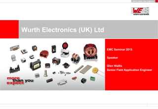
  • 1. Wurth Electronics (UK) Ltd 1 EMC Seminar 2015 Speaker Glen Wallis Senior Field Application Engineer
  • 2. Agenda - What is EMC? - Magnetic and Material Basics - Transmission Modes & Filter Topologies - Component Solutions - Design Guides 2
  • 4. EMC Standards and tests are seen by customers as HUGE PROBLEMS
  • 5. Economical point of view: Cost Pre-design Prototype Production Time EMC Effect • dependent on when EMC conformity is considered in a design phase
  • 6. EMC, what frequency range does it cover? 6
  • 9. Mai 10 AR 9 Electromagnetic Wave
  • 10. EMC – Electromagnetic Wave 1 cycle = 0o to 360o 360o Frequency (F) = 1 / Period = 1 / 20uS = 50 kHz Wavelength (λ) = Speed of Light (m/s) / Frequency = 3x10⁸ / 50x103 = 6000 metres 20us 0S Period (S) = 0 seconds to 20uS 0o Electric field Magnetic field
  • 11. The magnetic field Each electric powered wire generates an electro magnetic field Field model current I Magnetic field H
  • 13. 13 The magnetic field - Field model
  • 14. Magnetic Fields – The magnetic field
  • 15. N O R T H S O U T H Magnetic field H Current I 15 The magnetic field – Field Model
  • 16. R I mAH   2 )/( R IN mAH    2 )/( l IN mAH  )/( Straight wire Toroidal l R R solenoid I = Current N = Number of turns R = Radius L= Length H (A/m) = Field strength (A/m) 16 The magnetic field
  • 17. R I mAH   2 )/( R IN mAH    2 )/( Straight wire Toroidal R R The magnetic field strength is depending from: • Geometries • No. of turns • Current 17 But NOT MATERIAL e.g I = 5A, R = 0.2, N =10 =5 / 2 x 3.14 x 0.2 =3.978 A/m =10 x 5 / 2 x 3.14 x 0.2 =39.78 A/m The magnetic field
  • 18. averageR I HHH   2 21 1B 2B?   Current I averageR 1H 2H averageR The magnetic field
  • 19. What is permeability? • un ordered (random position) • soft magnetic • ordered • hard magnetic Ferrite material Permanent magnet Relative permeability • describe the capacity of concentration of the magnetic flux in the material. • it is a energy factor to magnetize the material Typical permeability µr : • Iron power : • Nickel Zinc : • Manganese Zinc : 50 ~ 150 40 ~ 1500 300 ~ 20000 19
  • 20. -50 50 150 250 1000 T / °C 500 540 670 770 +15 % -20 % - The magnetization depends from the temperature T therm. movement Alignment Alignment of elementary magnets Ferromagnetic change to Paramagnetic Point reached at µr = ?1 -40°C 23°C 85°C Curie-temperature Temperature influnce µr Permeability – Core material parameter 20
  • 21. Permeability – complex permeability =1 turn Core material-Parameter XL(NiZn) R(NiZn) Z X L__ 22 Z R R X L Z Replacement circuit 21
  • 22. 0% 10% 20% 30% 40% 50% 60% 70% 80% 90% 100% 0,01 0,1 1 10 100 1000 Core material – Inductors (Storage) f/MHz XL(NiZn)XL(MnZn)XL(Fe) Impedance 22
  • 23. 0% 10% 20% 30% 40% 50% 60% 70% 80% 90% 100% 0,01 0,1 1 10 100 1000 Core material – Choke (Filter) f/MHz R (NiZn)R (MnZn)R (Fe) Impedance 23
  • 24. Core Losses Electro Magnetic energy cannot disappear, it will be just transformed into other energy form energy conservation law e.g. electrical energy transformed into  thermal energy the core losses from ferrite transform the noise energy into heat
  • 26. Transmission modes Live (Positive) Earth (Ground)  Recognize the transmission mode: Differential Mode signals on a line(s) with a return path Common Mode noise on all lines propagating in the same direction with respect to earth Neutral (Return) Cs
  • 27. EMC - Coupling  Primary procedure …to aim at source a low noise  Secondary procedure … eliminate the noise thru interrupting the coupling way  Tertiary procedure … increase the noise immunity at load Noise source Load Coupling way
  • 28. Capacitive coupling • Effects are dominant when the dimensions are 10% below the wave length (l < /10) -> Why 1/10 ? -> Reduction ? - Increase the distance - harmonics Field model Network model EMC - Coupling
  • 29. Inductive coupling  Reduction? - Increase the distance • Antenna principle –> each piece of wire is a antenna fc   • Effects are dominant when the PCB traces are ca. 25% from the noise wave length (l < /4) Field model Network model EMC - Coupling
  • 30. Coupling - Wavelengths Frequency (MHz) Wavelength (m) H field 1/4 wavelength (m) E field 1/10 wavelength (m) 30 10 2.5 1 100 3 0.75 0.3 500 0.6 0.15 0.06 1000 0.3 0.075 0.03 2500 0.12 0.03 0.012 3000 0.1 0.025 0.01 6000 0.05 0.0125 0.005
  • 31. Recognizing the coupling mode  common mode noise ?  differential mode noise ?
  • 32. Common mode or differential mode? Take a Snap Ferrite and fix it on the cable (both lines e.g. VCC and GND) if noise is reduced or noise immunity increase you have Common Mode Interference If not you have Differential Mode Interference e.g. Common mode choke e.g. chip bead ferrite
  • 33. • Impedance BA BFA ZZ ZZZ A    log20 • System attenuation    BABA A F ZZZZZ        20 10 )(dBin )(in Insertion loss – Mathematical Definition LoadSource ZA ZF ZBU1U0 U2 Coupling way 33
  • 34. Insertion loss – recommended filter topology Pay attention to: SRF of used components  small C = higher SRF Choose ferrite bead or inductors L which = build no resonance with C = broadband filter Source Impedance Load Impedance low low low high high high high or unknow n low or unknow n low or unknow n C L CC L L C L high or unknow n
  • 35. Filter design How to?:  defined filter using 2 components  at least 1 component must be frequency dependant  Matching the working frequency for the signal  Matching the cut of frequency for the noise Filter input Z1 Z2 UE U A Filter output Conclusion: Filter are frequency dependant voltage divider 35
  • 36. Low pass filter …are most popular used filter for EMI UE U A L C 1UE U A LPF 1. rank LPF 2. rank C 1 R f ZC f ZL f ZC 36
  • 37. -40 -35 -30 -25 -20 -15 -10 -5 0 1 10 100 1000 Frequenz [MHz] Filter topologies – L-Filter • L-Filter Zmax= 3000 Ω @ 80 MHz • WE-CBF 742 792 093 AF = -29 dB @ 80 MHz Simulated Measured • instead of inductor use SMD-Ferrite
  • 38. -90 -81 -72 -63 -54 -45 -36 -27 -18 -9 0 1 10 100 1000 Frequenz [MHz] Filter topologies – Parallel-C-Filter • Parallel-C-Filter • Resonant freq.
  • 39. Filter topologies – LC-Filter • LC-Filter WE-CBF 742 792 093 C=100nF -90 -81 -72 -63 -54 -45 -36 -27 -18 -9 0 1 10 100 1000 Frequenz [MHz] Simulated Measured • Compare simulated vs. measured
  • 40. Design-Tip: avoid over current (load dump) Uin e.g. 12V DC SMD/Ferrite + Umax U(t) Imax I(t)  2 3 4 5  2 3 4 5 Filter topologies – LC-Filter
  • 41. Filter topologies – LC-Filter Uin e.g. 12V DC SMD/Ferrite + Design-Tip: avoid over load of bead ferrite! • Safety for SMD-Ferrite against low dump current • Not an PI-Filter  Capacity C1 is just for stabilizing
  • 42. Filter topologies – PI-Filter • Compare simulated vs. measured • π-Filter WE-CBF 742 792 093 C1=1nF C2=100nF -90 -81 -72 -63 -54 -45 -36 -27 -18 -9 0 1 10 100 1000 Frequenz [MHz] Simulated Measured
  • 43. Filter topologies – T-Filter • T-Filter C=100nF L1=742 792 040 L2=742 792 093 -90 -81 -72 -63 -54 -45 -36 -27 -18 -9 0 1 10 100 1000 Frequenz [MHz] Simulated Measured • Compare simulated vs. measured
  • 44. Common Mode Filter – Signal theories Transmitter/ Source Receiver/ Load differential common Data lines Noise mode: • Common mode noise • Differential mode noise D- D+ e.g.: USB 44
  • 45. It is a Bi-directional filter • From device to outside environment • From outside environment to inside device Conclusion: Common Mode Filter – How it works Intended Signal - Differential mode Interference Signal (noise) – Common Mode • “almost” no affect the signal - Differential mode • high attenuation to the interference signal (noise) – Common Mode
  • 46. Source LoadSignal path Common mode VCC GND D- D+ e.g.: USB Filtering WE-CNSW Type 0805 Common Mode Filter – Signal theories
  • 47. Filter with two inductors Filter input Filter output Filter with CMC Filter input Filter output • Signal not affected • Noise attenuated even close to the signal frequency Common mode choke - advantages
  • 48. USB1.0 IC USB1.0 IC Spektrum -80 -70 -60 -50 -40 -30 -20 -10 0 0 500 1000 1500 2000 2500 3000 Frequenz in MHz LeistungindBm D+ D- D+ D-  filtered  un filtered  Tx signal RF-Generator Common Mode Choke Common Mode Choke  Data source Common mode choke – application USB
  • 49. 32 Ohm 0.7 Ohm Increase ZFail rate: 3.4% Fail rate: 2.55% Fail rate: 0% Fail rate: 2.05% @ 12 MHz CM  DM  41 Ohm 0.7 Ohm @ 12 MHz CM  DM  363 Ohm 1 Ohm @ 12 MHz CM  DM  77 Ohm 1 Ohm @ 12 MHz CM  DM  Common Mode Choke D+ D- D+ D- Increase Z Common mode choke - construction
  • 50. SMD-Ferrite – application USB Fail rate: 0‰ Fail rate: 4.4% Fail rate: 7.5% 35 Ohm @ 12 MHzDM  110 Ohm @ 12 MHzDM  Using an WE-CBF instead of CMC 2 x SMD-Ferrit D+ D- D+ D- Increase Z
  • 52. How to resolve EMI using EMC counter measures 52
  • 53. PCB mounted EMC ferrites  Ideal time is to design these series of components in at the product design stage  Why? The benefits are as follows: 1. Small package size, thus footprint. 2. Saving valuable PCB space 3. Allows for positioning close to the EMI source or point of filtering
  • 54. PCB mounted EMC ferrites- Key points  Applications - DC power line filtering - Low voltage AC power line filtering - Data/Signal line filtering  EMC Phenomena – Radiated Emission – Radiated Immunity – Conducted Emissions – Conducted Immunity – Electro Static Discharge (ESD) – Electric Fast Transients (EFT)
  • 55. PCB mounted EMC ferrites  Majority are Differential mode filters – WE-CBF – WE-CBF HF – WE-MPSB – WE-PBF – WE-PF – WE-SUKW – WE-UKW – WE-WAFB  Maximum operating voltage - 80Vdc - 42Vac
  • 56. PCB mounted EMC ferrites WE-CBF (Chip Bead Ferrites) Three types in the series High Speed Wide Band High Current
  • 57. WE-CBF vs WE-CBF HF Both are 0603 package size, Z = 1k Ω @ 100MHz WE-CBF WE-CBF HF WE-CBF HF has greater than 3 times the impedance at 1GHz
  • 59. Retro fit EMC ferrites - Key points  Applications - AC power line filtering - DC power line filtering - Data/Signal line filtering  EMC Phenomena – Radiated Emission – Radiated Immunity – Conducted Emissions – Conducted Immunity – Electric Fast Transients (EFT)
  • 60. Retro fit EMC ferrites  These components are design to be fitted to cables or cable harnesses  These are all Split ferrites. Design for quick application to the cable  * Use a unique ‘key’ system that reduced unauthorised removal of the ferrite Snap ferrite sleeve Snap ferrite ring WE-NCF Split EMI ferrite ring Split EMI flat ferrite STAR-BUENO * STAR-FIX * STAR-LFS * STAR-TEC * STAR-GAP * STAR-RING * STAR-FLAT * Only manufacturer to offer this key system
  • 61. Retro fit EMC ferrites Mai 10 AR 61 STAR – xxx series FIX - LFS TEC / RING /FIX GAP
  • 62. 12 1 10 23 100 0 200 400 600 800 1000 1200 1400 1600 1800 2000 1 10 100 1000 f/MHz Retro fit EMC ferrites – Number of turns MnZn NiZn  2 turns
  • 63. Retro fit EMC ferrites  These ferrites are defined as solid core WE-SFA WE-FLAT WE-FAP WE-FLAT (Flexible PCB) WE-TOF WE-AFB WE-AFB LFS WE-SAFB Mutli-Aperture ferrite  Used largely to replace the split ferrites used during EMC testing  Have to be applied to the cable/cable harness prior to any connectors are crimped to the ends of the cables  These components are design to be fitted to cables and cable harnesses
  • 64. Where do we place the ferrite ? Design:  As close as possible to the source of the noise Ideally 20mm to 50mm from the point of cable connectivity
  • 65. Recognizing the coupling mode  common mode noise ?  differential mode noise ?
  • 66. How can we find out what interference we have? Common mode or differential mode? Take a Snap Ferrite and fix it on the cable (both lines e.g. VCC and GND) if noise is reduced or noise immunity increase you have Common Mode Interference If not you have Differential Mode Interference e.g. Common mode choke e.g. chip bead ferrite
  • 67. • Impedance BA BFA ZZ ZZZ A    log20• System attenuation    BABA A F ZZZZZ        20 10 )(dBin )(in Insertion loss - Definition LoadSource ZA ZF ZBU1U0 U2 Coupling way
  • 68. >90  1  10  System Impedances
  • 69. 1  50 - 90  10  System Impedances
  • 70. The problem  Example, Radiated Emission plot
  • 71. Mai 10 AR 71 Quick Solution Impedance of ferrite (Ω) Attenuation(dB) 1. 1.Require 20dB of attenuation at 125 MHz 2. Know that it is a power cable 3. Power port has 10 Ω impedance 180 • Result is a minimum impedance of 180Ω
  • 72. The result  Example with Ferrite fitted Example, Radiated Emission plot
  • 74. Current compensated common mode chokes - Key points  Applications – Power line - AC power line (110 to 250Vac rms) filtering - DC power (<250V) line filtering  Applications – Signal/Data line - Low voltage (<42V) AC power line filtering - DC power (<80V) line filtering - Data/Signal line filtering  EMC Phenomena – Radiated Emission – Radiated Immunity – Conducted Emissions – Discontinuous Conducted Emissions – Conducted Immunity
  • 75. Common mode choke - construction bifilar sectional
  • 76. Data/Signal lines Common mode chokes  Rated at 80Vdc or 42Vac (except WE-CNSW 50Vdc) WE-CNSW – 0603, 0805 & 1206 sizes. Bifilar wound WE-SLM - Bifilar wound WE-SL1 – Sectional wound WE-SL2 - Bifilar wound & Sectional wound (denoted with a S) WE-SL3 - Either 2 or 3 wire. Bifilar or Trifilar wound WE-SL5 - Maximum current 2.5A Bifilar wound & Sectional wound (denoted with a S) WE-SL5HC - Maximum current 5A Sectional wound WE-SL – Either 2 or 4 wire. Bifilar or Quadfilar wound
  • 77. P/N: EP-CBF-0805  SMD Ferrite 0805 EP-CBF-1206  SMD Ferrite 1206 EP-STROKO  WE-SLxy… Series SMD common mode chokes VPE 12 pcs.  Price £20 inclusive P&P Application demo boards
  • 78. Common mode chokes – Power lines  Rated at 250Vac rms @ 50/60Hz, maximum current is 35A  Also possible to pass high current DC through them  WE-CMB  WE-CMB HC  WE-CMB NiZn*  WE-LF  WE-LF SMD  WE-FC Mini  WE-FC  WE-TFC  Used for low frequency suppression in the frequency range of 150KHz to 30MHz.  * 30MHz to 300MHz due to NiZn core
  • 79. Common mode chokes – line card Insertion loss (common mode) WE-CMB XS: MnZn <=> NiZn 0 10 20 30 40 50 60 70 0,1 1 10 100 1000 frequency [MHz] attenuation[dB] 14 µH 30 µH 47 µH 100 µH 1 mH 5 mH 10 mH 20 mH 39 mH CMB NiZnCMB MnZn
  • 80. Nano Crystalline – WE-CMBNC 80
  • 82. WE-CMB Impedance vs Temperature 82 1 10 100 1000 10000 100 1000 10000 100000 Impedance(Ohm) f (kHz) CMB @ -40 CMB @ 80 CMB @ 120 CMB @ 150 CMB @ 180 2014-02-24 / IMA
  • 83. WE-CMBNC Impedance vs Temperature 83 1 10 100 1000 10000 100 1000 10000 100000 Impedance(Ohm) f (kHz) CMBNC @ -40 CMBNC @ 80 CMBNC @ 120 CMBNC @ 150 CMBNC @ 180 2014-02-24 / IMA
  • 84. Cost saving? Insertion loss (common mode) WE-CMB XS: MnZn <=> NiZn 0 10 20 30 40 50 60 70 0,1 1 10 100 1000 frequency [MHz] attenuation[dB] 14 µH 30 µH 47 µH 100 µH 1 mH 5 mH 10 mH 20 mH 39 mH CMB NiZnCMB MnZn CMB NC
  • 85. Circuit Protection – Key points  Applications - AC power line (14 to 1000Vac rms) protection - DC power line (18 to 1465Vdc) protection - Signal/Data line protection  EMC Phenomena – Electro Static Discharge (ESD) – Electrical Fast Transients (EFT) – High Energy Surges (HES) The EMC phenomena can be defined as a transient event, a phenomena that's presence is not constant  These products are for protection against over voltages
  • 86. Why do we need circuit protection? Mai 10 AR 86
  • 87. Circuit Protection  What is an over voltage? Typically 500V to 15kV AC voltage 230V ± 10% Over voltage > 260V
  • 88. Circuit Protection  The following components are WE-TVS Standard Series WE-TVS High Speed Series WE-TVS Super speed Series WE-VE WE-VE ULC WE-VEA WE-VEA ULC WE-VS WE-VD
  • 89. Circuit Protection – ESD/EFT  TVS Diodes – Transient Voltage Suppressors  WE-TVS Standard Series Application = USB 1.1 (12Mbps)  WE-TVS High Speed Series Application = USB 2.0 (480Mbps)  WE-TVS Super speed Series Application = USB 3.0 (4.8Gbps) These devices can be used to protect the DC power and also the signal lines in one package
  • 90. Waveshape - ESD  ESD  Maximum rise time = 1ns  Duration = approx 40ns  Maximum pk I (8kV) = 30A Mai 10 AR 90
  • 91. Waveshape - EFT  FTB/EFT  Rise time 5nS  Duration 50ns Mai 10 AR 91
  • 92. Circuit Protection - TVS  What do I need to know to be able to select one?
  • 93. USB – 2 Port solution (ESD/EFT solution) Mai 10 AR 93
  • 94. USB – 2 Port solution (ESD/EFT-EMI solution) Mai 10 AR 94
  • 96. Circuit Protection - ESD  The WE-VE series of components are suited for the ultra fast voltage pulses caused by Electro Static Discharge  The following components are WE-VE WE-VE ULC (Ultra Low capacitance) WE-VEA WE-VEA ULC (Ultra Low capacitance)  These devices are applied to the DC power and also signal/data lines
  • 97. Circuit Protection - ESD  What do I need to know to be able to select one?
  • 99. Mai 10 AR 99 USB 2.0 filter dongle P/N 829999 BAG
  • 100. Mai 10 AR 100 WE-USBH Connector with Integrated EMI & ESD function Full Speed – 480MHz P/N 8492121
  • 101. Mai 10 AR 101 WE-USBH Connector with Integrated EMI & ESD function
  • 102. Circuit Protection - HES  Surge protection devices  WE-VS Application - AC power line (4 to 40Vac rms) protection - DC power line (5.5 to 56Vdc) protection  WE-VD Application - AC power line (14 to 1000Vac rms) protection - DC power line (18 to 1465Vdc) protection
  • 103. What size of varistor to select?  Vrms or Vdc  Peak I (A)  Wmax (J)  Pdiss (W) It is necessary to calculate (estimate) the maximum surge current that could flow through the varistor Parameters to consider: Operating Voltage Maximum withstand surge current Maximum energy absorption Maximum Power dissipation
  • 104. Surge Test - Waveforms Mai 10 AR 104 Test waveforms as specifed by the test method EN 61000-4-5:2006: Open Circuit Rise Time : 1.2 µs Duration : 50 µs Short Circuit Rise Time : 8 µs Duration : 20 µs
  • 105. Varistor Characteristics – V I Curve +U +I VVar VCVM IL IVar Ic IMax Max. Operating Voltage Clamping Voltage Leakage Current 0,1mA or 1mA Current @ Clamping Voltage U-I Graph for SMD-Varistor 825 42 350 0 1 2 3 4 5 6 7 30 40 50 60 70 Voltage [V] Current[mA] max. Current Varistor Breakdown Voltage
  • 106. EUT  Common Mode Z = 12Ω E Power lines L1 L2 L3 Signal lines  Differential Mode Z = 2Ω  Signal lines Z = 42Ω Surge Test - Application
  • 107. Calculation of the current: Ic  According to Ohms Law Surge Voltage (kV) Z (Ohms) Supply Voltage (Vpk) Surge Clamping Ic Impedance of the generator according to the type of port (Power or Signal) I load I load is negligible =>
  • 108. Method 2  Second Method ( estimation)  Vclamp ~ 2*V breakdown 7mm Disk Varistor VRMS 275 V V breakdown : 430V 14mm Disk Varistor VRMS 275 V V breakdown : 430V
  • 110. Calculation of the Energy Absorption • The energy in Joules (Watt per second) is given by the following formula: W (J) = K * V (V) * I (A) * t (s) Surge Clamping I Max • It can be difficult to make an exact calculation of the energy. • We can make an approximation, in considering rectangular wave. • V = Vclamp (just calculated before) • I = Ic ( just calculated) • T = 20µS ( time duration of the surge current) W (J) = Vclamp(V) • Ic (A) • 20µ(s) 50µs 20µs T(s) Surge Voltage Surge Current
  • 111. Calculation of the Power dissipation 
  • 113. Circuit Protection - MOV  What do I need to know to be able to select one?
  • 114. Derating curve according to the number of applied pulses Numberofsurges Example: Surge spaced 30 seconds. Time (s) Temperature(C)
  • 115. Layout of varistor for surge protection  Safety standards disapprove for varistors to Earth  Also the product likely to fail the Hi-pot, earth leakage test  If using fuses they must be suitable rated against surges. i.e Anti-Surge (T) FAE Dez. 2011
  • 116. UL 1449 3rd Edition  The WE-VD are typically designed into a product to protect against an overvoltage situation that could potential damage the product  It therefore makes the WE-VD are “safety critical component”  Underwriters Laboratory Inc. (UL) is a US based testing and Certification organisation  UL 1449 3rd Edition is a safety standard for circuit protection devices  Has four classes listed Type 1 – Protection of the mains distribution network Type 2 – Protection of permanent connected devices the mains distribution network Type 3 - Protection of non permanent connected devices the mains distribution network Type 4 – Discrete components  WE-VD are approved for Type 2, 3 & 4
  • 117. EMI Shielding material  The products can be constructed of two classes of material when it comes to RF: 1. Metallic – Aluminium, Steel, Brass, Copper Natural shielding material 2. Non Metallic – Plastic, Nylon, Polystyrene, PVC. RF transparent materials
  • 118. EMI Shielding material – Key points  Applications Shielding of non metallic enclosures Bonding of metallic enclosures Absorbing (Attenuating)  EMC Phenomena – Radiated Emissions – Radiated Immunity  Effective frequency range – 30MHz to 18GHz
  • 119. EMI Shielding material  WE-LT- RF gasket  WE-LTS – Stamped gasket  WE-LS – Conductive foam  WE-ST – Conductive weave  WE-CF – Copper tape. Largest user of copper tape are the EMC Labs  WE-TS – Textile tape
  • 120. EMI Shielding material  Earthing cable connectors  Earthing nylon clips  Earthing belts  WE-FAS EMI  WE-FAS RFID  WE-FSFS  WE-SECF  WE-SHC
  • 121. EMI Shielding material RF Gasket, WE-LT and WE-GS can be used in the following configurations to establish a good bond To enable good electrical conductivity, gasket must make direct metal work to metal work contact Any painted surface will act as an insulator (high resistance to RF)
  • 122. EMI Shielding material  Surface resistance
  • 125. Ethernet EMI solution: WE-RJ45 HPLE
  • 126. Leakage inductance shielded vs. unshielded
  • 127. Radiation by inductor WE - PD2 unshielded 10µH, 2MHz clock, 1A
  • 128. Radiation by inductor WE – PD shielded 10µH, 2MHz clock, 1A 19dBm improvement
  • 129. • consider start of winding Inductors are two poles only  but start of winding is important  use effect of self shielding of the winding connection switch node “EMI hot side” Self sheilding
  • 131. Catalogue EMC Components Power Magnetics Signal & Communications Additional technical drawing data supplied (inc. tolerances) Also addition of QR codes
  • 132. Trilogy of Magnetics Now published as 4th edition Three sections:- Magnetic basics Components Application notes Filtering DC/DC PSU design
  • 133. Design Tools LT Spice Simulator WE Component Selector Inductor Selector WE-Flex transformer designer RF inductor Selector Chip Bead Ferrite Selector