Download to read offline

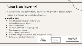
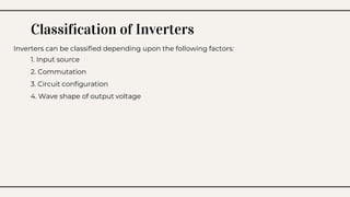
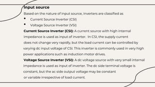
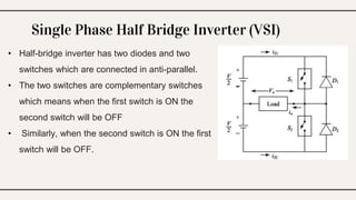
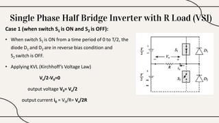
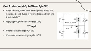
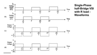
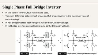
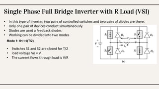
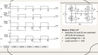
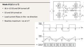
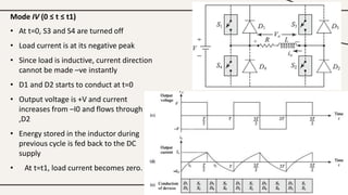
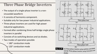
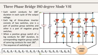
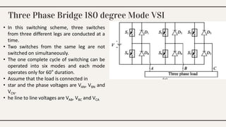
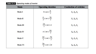
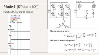
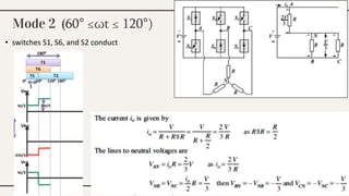
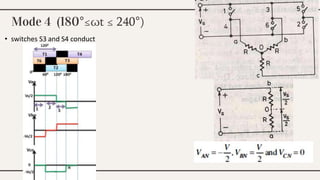
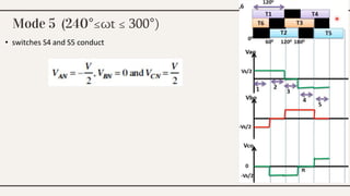
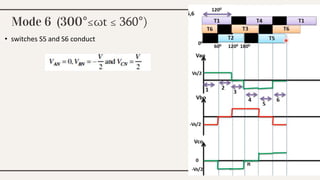
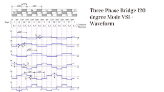
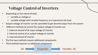
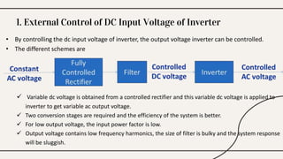
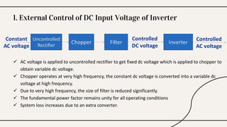
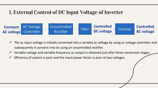
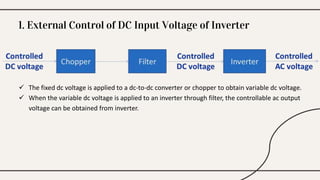
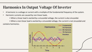
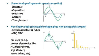
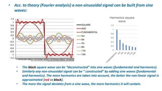
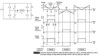
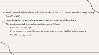
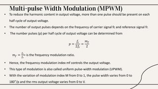
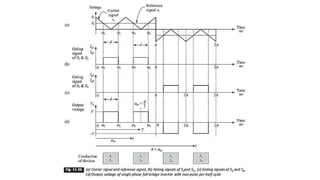
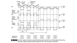
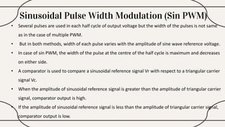
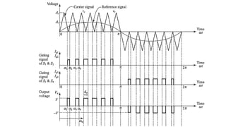
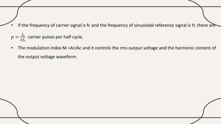
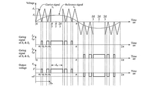
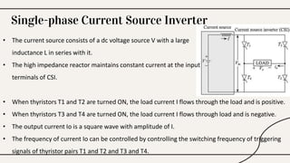
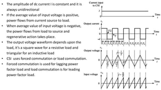
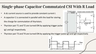
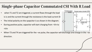
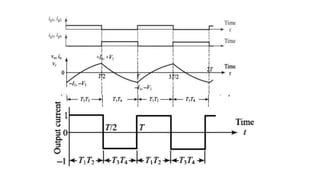
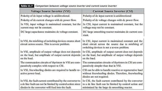


The document discusses inverters, which are static devices that convert DC power into AC power, detailing their applications, classifications, and types including current source and voltage source inverters. It also explains various circuit configurations and commutation methods, as well as operational modes for single-phase and three-phase inverters. Additionally, it covers voltage control methods for inverters, highlighting external and internal control techniques to achieve desired output voltages.


