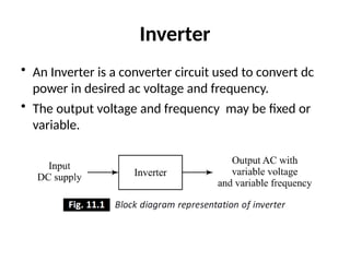
Inverter
• An Inverteris a converter circuit used to convert dc
power in desired ac voltage and frequency.
• The output voltage and frequency may be fixed or
variable.
3.
Inverters are mostcommonly used in the following
applications:
• Variable speed induction motor drives
• Adjustable speed ac drives
• Induction heating
• Uninterruptible power supply (UPS)
• Standby power supply
• HVDC power transmission
• Variable voltage and variable frequency power supply
• Battery operated vehicle drives
Inverter Applications
4.
Inverters can beclassified depending upon the following
factors:
• Input source
• Commutation
• Circuit Configuration
• Wave Shape of Voltage
Classification of Inverters
5.
Based on thenature of input source Inverters can be
classified as :
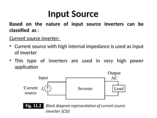
Current source inverter:
• Current source with high internal impedance is used as input
of inverter
• This type of inverters are used in very high power
application
Input Source
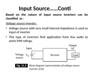
6.
Based on thenature of input source Inverters can be
classified as :
Voltage source inverter:
• Voltage source with very small internal impedance is used as
input of inverter
• This type of inverters find application from few watts to
some MW ratings.
Input Source……Conti
7.
Commutation
According to commutationmethod, inverters may be classified
as line commutated inverters or forced commutated inverters:
• Line commutated inverters
• Forced commutated inverters
• Auxiliary Commutated inverters
• Complementary commutated inverters
8.
Circuit Configuration
According tocircuit topology inverters can be classified as:
• Series inverters: L and C are connected in series with the load and the
performance of the inverter depends upon commutating components
i.e. L&C
• Parallel inverters: : L and C are connected in parallel with the load
• Half bridge and full bridge inverters: In half bridge only one leg of
bridge exists. In full bridge two or three legs are existing for 1-phase or
3-phase inverters respectively.
9.
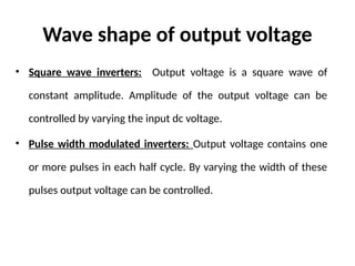
Wave shape ofoutput voltage
• Square wave inverters: Output voltage is a square wave of
constant amplitude. Amplitude of the output voltage can be
controlled by varying the input dc voltage.
• Pulse width modulated inverters: Output voltage contains one
or more pulses in each half cycle. By varying the width of these
pulses output voltage can be controlled.
10.
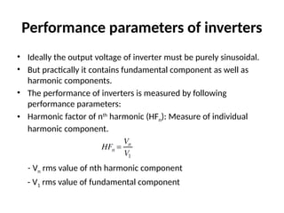
Performance parameters ofinverters
• Ideally the output voltage of inverter must be purely sinusoidal.
• But practically it contains fundamental component as well as
harmonic components.
• The performance of inverters is measured by following
performance parameters:
• Harmonic factor of nth
harmonic (HFn): Measure of individual
harmonic component.
- Vn rms value of nth harmonic component
- V1 rms value of fundamental component
11.
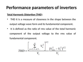
Total Harmonic Distortion(THD):
• THD It is a measure of closeness in the shape between the
output voltage wave form and its fundamental component.
• It is defined as the ratio of rms value of the total harmonic
component of the output voltage to the rms value of
fundamental component.
Performance parameters of inverters
12.
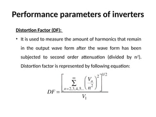
Distortion Factor (DF):
•It is used to measure the amount of harmonics that remain
in the output wave form after the wave form has been
subjected to second order attenuation (divided by n2
).
Distortion factor is represented by following equation:
Performance parameters of inverters
13.
Lowest order harmonics(LoH):
• It is the lowest frequency harmonic with a magnitude
greater than or equal to three percent of the magnitude of
the fundamental component of out put voltage.
• For higher frequency of LoH the distortion will be lower in
the current waveform.
Performance parameters of inverters
14.
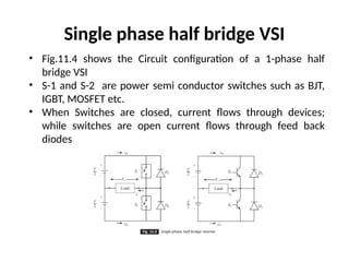
Single phase halfbridge VSI
• Fig.11.4 shows the Circuit configuration of a 1-phase half
bridge VSI
• S-1 and S-2 are power semi conductor switches such as BJT,
IGBT, MOSFET etc.
• When Switches are closed, current flows through devices;
while switches are open current flows through feed back
diodes
15.
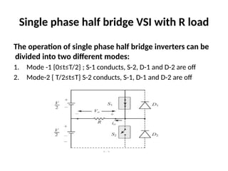
Single phase halfbridge VSI with R load
The operation of single phase half bridge inverters can be
divided into two different modes:
1. Mode -1 {0≤t≤T/2} ; S-1 conducts, S-2, D-1 and D-2 are off
2. Mode-2 { T/2≤t≤T} S-2 conducts, S-1, D-1 and D-2 are off
16.
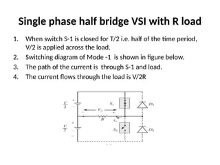
Single phase halfbridge VSI with R load
1. When switch S-1 is closed for T/2 i.e. half of the time period,
V/2 is applied across the load.
2. Switching diagram of Mode -1 is shown in figure below.
3. The path of the current is through S-1 and load.
4. The current flows through the load is V/2R
17.
Single phase halfbridge VSI with R load
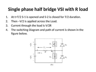
1. At t=T/2 S-1 is opened and S-2 is closed for T/2 duration.
2. Then –V/2 is applied across the Load.
3. Current through the load is V/2R
4. The switching Diagram and path of current is shown in the
figure below.
18.
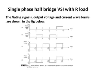
Single phase halfbridge VSI with R load
The Gating signals, output voltage and current wave forms
are shown in the fig below:
19.
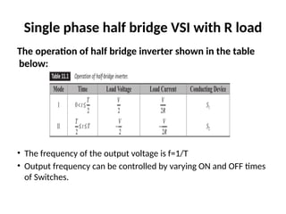
Single phase halfbridge VSI with R load
The operation of half bridge inverter shown in the table
below:
• The frequency of the output voltage is f=1/T
• Output frequency can be controlled by varying ON and OFF times
of Switches.
20.
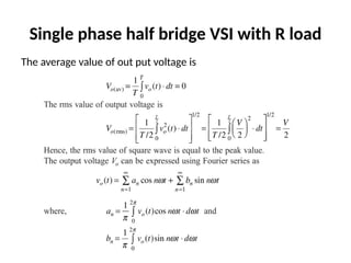
Single phase halfbridge VSI with R load
The average value of out put voltage is
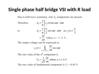
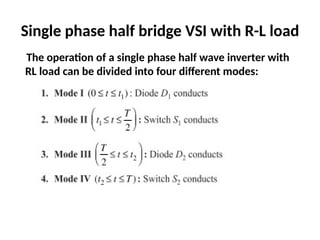
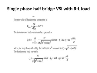
Single phase halfbridge VSI with R-L load
The operation of a single phase half wave inverter with
RL load can be divided into four different modes:
23.
Single phase halfbridge VSI with R-L load
Mode –I (0 ≤ t ≤ t1):
• At t=0, gating signal is removed from S2, it becomes off.
• At this instant load current io, isequal to its negative peak value
• Due to inductive load current does not change instantaneously,
Hence D1 start to conduct at t=0
• Subsequently voltage across the load is V/2 and load current io,
increases from negative peak i.e. –Io
• Load current flows through D1
• Voltage across the load is positive but load current is negative
• Hence the energy stored in the inductor L during previous cycle
is fed back to dc supply through D1
24.
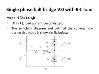
Single phase halfbridge VSI with R-L load
Mode –I (0 ≤ t ≤ t1):
• At t= t1, load current becomes zero
• The switching diagram and path of the current flow
during this mode is shown in fig below:
25.
Single phase halfbridge VSI with R-L load
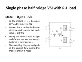
Mode –II (t1 ≤ t ≤ T/2):
• At the instant t= t1 D1 becomes
OFF and S1 is turned ON
• Current Starts to flow in the +ve
direction and reaches +ve peak
value Io at t=T/2
• During this interval both Voltage
and Current are +ve and energy
is stored in the inductor L.
• The switching diagram and path
of the current flow during this
mode is shown in fig(b):
26.
Single phase halfbridge VSI with R-L load
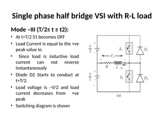
Mode –III (T/2≤ t ≤ t2):
• At t=T/2 S1 becomes OFF
• Load Current is equal to the +ve
peak value Io
• Since load is inductive load
current can not reverse
instantaneously
• Diode D2 Starts to conduct at
t=T/2.
• Load voltage is –V/2 and load
current decreases from +ve
peak
• Switching diagram is shown
27.
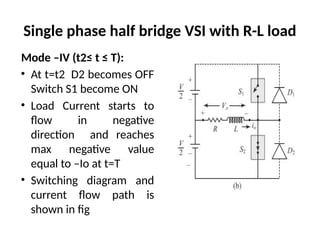
Single phase halfbridge VSI with R-L load
Mode –IV (t2≤ t ≤ T):
• At t=t2 D2 becomes OFF
Switch S1 become ON
• Load Current starts to
flow in negative
direction and reaches
max negative value
equal to –Io at t=T
• Switching diagram and
current flow path is
shown in fig
28.
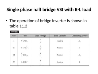
Single phase halfbridge VSI with R-L load
• The operation of bridge inverter is shown in
table 11.2
29.
Single phase halfbridge VSI with R-L load
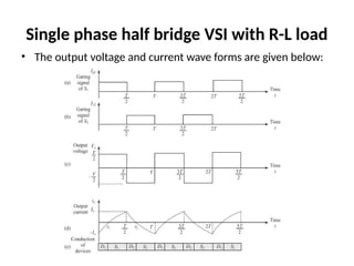
• The output voltage and current wave forms are given below:
30.
Single phase halfbridge VSI with R-L load
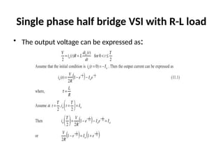
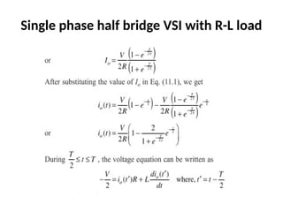
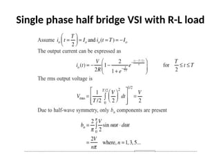
• The output voltage can be expressed as: