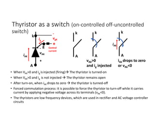
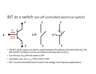
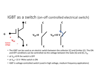
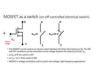
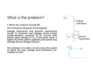
power electronics ssssssssssssssssssssssssssssssssssssssssssssssssssssssssssssssssssssssssssssssssssssssssssssssssssssssssssssssssssssssssssssssssssssssssssssssssssssssssssssssssssssssssssssssssssssssssssssssssssssssssssssssssssssssssssssssssssssssssssssssssssssssssssssssssssssssssssssssssssssssssssssssssssssssssssssssssssssssssssssssssssssssssssssssssssssssssssssssssssssssssssssssssssssssssssssssssssssssssssssssssssssssssssssssssssssssssssssssssssssssssssssssssssssssssssssssssssssssssssssssssssssssssssssssssssssssssssssssssssssssssssssssssssssssssssssssssssssssssssssssssssssssssssssssssssssssssssssssssssssssssssssssssssssssssssssssssssssssssssssssssssssssssssssssssssssssssssssssssssssssssssssssssssssssssssssssssssssssssssssssssssssssssssssssssssssssssssssssssssssssssssssssssssssssssssssssssssssssssssssssssssssssssssssssssssssssssssssssssssssssssssssssssssssssssssssssssssssssssssssssssssssssssssssssssssssssssssssssssssssssssssssssssssssssssssssssssssssssssssssssssssssssssssssssssssssssssssssssssssssssssssssssssssssssssssssssssssssssssssssssssssssssssssssssssssssssssssssssssssssssssssssssssssssssssssssssssssssssssssssssssssssssssssssssssssssssssssssssssssssssssssssssssssssssssssssssssssssssssssssssssssssssssssssssssssssssssssssssssssssssssssssssssssssssssssssssssssssssssssssssssssssssssssssssssssssssssssssssssssssssssssssssssssssssssssssssssssssssssssssssssssssssssssssssssssssssssssssssssssssssssssssssssssssssssssssssssssssssssssssssssssssssssssssssssssssssssssssssssssssssssssssssssssssssssssssssssssssssssssssssssssssssssssssssssssssssssssssssssssssssssssssssssssssssssssssssssssssssssssssssssssssssssssssssssssssssssssssssssssssssssssssssssssssssssssssssssssssssssssssssssssssssssssssssssssssssssssssssssssssssssssssssssssssssssssssssssssssssssssssssssssssssssssssssssssssssssssssssssssssssssssssssssssssssssssssssssssssssssssssssssssssssssssssssssssssssssssssssssssssssssssssssssssssssssssssssssssssssssssssssssssssssssssssssssssssssssssssssssssssssssssssssssssssssssssssssssssssssssssssssssssssssssssssssssssssssssssssssssssssssssssssssssssssssssssssssssssssssssssssssssssssssssssssssssssssssssssssssssssssssssssssssssssssssssssssssssssssssssssssssssssssssssssssssssssssssssssssssssssssssssssssssssssssssssssssssssssssssssssssssssssssssssssssssssssssssssssssssssssssssssssssssssssssssssssssssssssssssssssssssssssssssssssssssssssssssssssssssssssssssssssssssssssssssssssssssssssssssssssssssssssssssssssssssssssssssssssssssssssssssssssssssssssssssssssssssssssssssssssssssssssssssssssssssssssssssssssssssssssssssssssssssssssssssssssssssssssssssssssssssssssssssssssssssssssssssssssssssssssssssssssssssssssssssssssssssssssssssssssssssssssssssssssssssssssssssssssssssssssssssssssssssssssssssssssssssssssssssssssssssssssssssssssssssssssssssssssssssssssssssssssssssssssssssssssssssssssssssssssssssssssssssssssssssssssssssssssssssssssssssssssssssssssssssssssssssssssssssssssssssssssssssssssssssssssssssssssssssssssssssssssssssssssssssssssssssssssssssssssssssssssssssssssssssssssssss


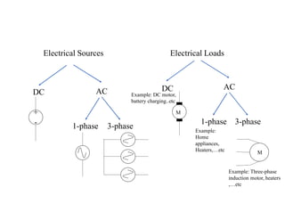
![Industrial/Power Electronics Converters
DC AC
Inverters
Rectifiers
AC voltage
Controllers
-On/Off control
-phase angle control
DC choppers
-Buck Vout=DVin
-Boost Vout=Vin/[1-D]
-Buck Boost |Vout|=D*Vin/[1-D]
D: controlled switch duty cycle 0<D<1](https://image.slidesharecdn.com/4thpowerpeapps-250317150423-64c6a466/85/4th_power_PE-App-enginering-electricql-pdf-5-320.jpg)


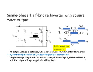
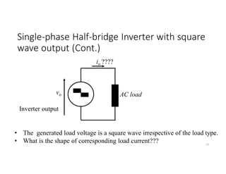
![Single-phase Half-bridge Inverter with square
wave output (Cont.)
In case of inductive load (RL with τ = L/R):
Based on the step response of the 1st order RL
circuit, load current peak is given by;
Imax= (Vd/2R)*[(1-e-T/2τ)/(1+e-T/2τ)]
vo +Vd/2
-Vd/2
t
io
t
po
t
D2
T1
D1 T2 D1 T1
iD1
T/2 T
+Imax
-Imax
iT1
32](https://image.slidesharecdn.com/4thpowerpeapps-250317150423-64c6a466/85/4th_power_PE-App-enginering-electricql-pdf-32-320.jpg)
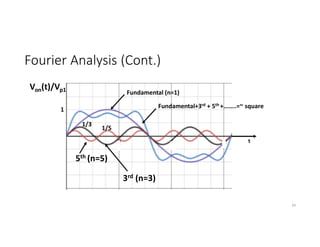
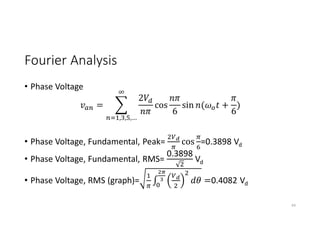
![Fourier Analysis
vo +Vd/2
-Vd/2
t
T/2 T
Odd function
Fundamental
component
Harmonics
(not desired) 33
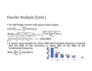
• The square-wave output of the single phase half-bridge inverter can be
extracted to summation of sinusoidal functions using Fourier series.
• vo(t)=∑ Vpn sin (nωot)
, , ,..
Where ωo is the fundamental angular velocity (rad/s),
Vpn=peak voltage of nth harmonics= ∫ ( )∗sin (nωot) dωot
i.e. , Vpn=
2Vd
nπ
• vo(t)=
2Vd
π
[sin (ωot) + sin (3ωot)+ sin (5ωot)+……]](https://image.slidesharecdn.com/4thpowerpeapps-250317150423-64c6a466/85/4th_power_PE-App-enginering-electricql-pdf-33-320.jpg)

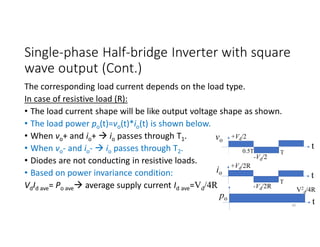
![Single-phase Half-bridge Inverter with square
wave output (Cont.)
In case of inductive load (RL with τ = L/R):
Based on the step response of the 1st order RL
circuit, load current peak is given by;
Imax= (Vd/R)*[(1-e-T/2τ)/(1+e-T/2τ)]
vo +Vd
-Vd
t
io
t
T/2 T
+Imax
-Imax
47](https://image.slidesharecdn.com/4thpowerpeapps-250317150423-64c6a466/85/4th_power_PE-App-enginering-electricql-pdf-47-320.jpg)
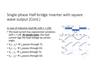
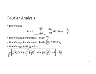
![Fourier Analysis
vo +Vd
-Vd
t
T/2 T
Odd function
Fundamental
component
Harmonics
(not desired)
48
• vo(t)=∑ Vpn sin (nωot)
, , ,..
Vpn=peak voltage of nth harmonics= ∫ ∗sin (nωot) dωot
i.e. , Vpn=
4Vd
nπ
• vo(t)=
4Vd
π [sin (ωot) + sin (3ωot)+ sin (5ωot)+……]](https://image.slidesharecdn.com/4thpowerpeapps-250317150423-64c6a466/85/4th_power_PE-App-enginering-electricql-pdf-48-320.jpg)


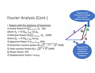
![Example
• Find the switching and conduction losses of single-phase half-bridge
inverter feeding resistive load of 10 Ω where Vd=200V, ton=toff=1 µs ,
on-state voltage of IGBT = 2V, On-state resistance of IGBT=5 mΩ and
switching frequency of 1kHz.
Solution:
• Ps per switch = 0.5IoVo fs(ton+ toff)=0.5(Vd/2R)(Vd) fs(ton+ toff)
• PC per switch = Von Iswitch average + I2
switch RMS Ron=
Von [0.5(Vd/2R)] + [0.5(Vd/2R)2]Ron
86](https://image.slidesharecdn.com/4thpowerpeapps-250317150423-64c6a466/85/4th_power_PE-App-enginering-electricql-pdf-86-320.jpg)


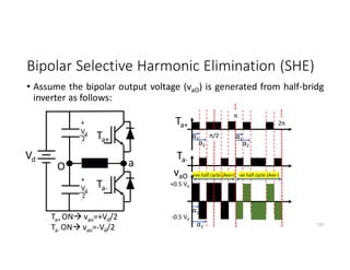
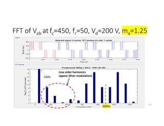
![Bipolar Selective Harmonic Elimination (Cont.)
The Fourier analysis for the shown output
voltage is given by;
Vpn= ∫ sin −
∫ sin + ∫ sin
/
i.e.,
Vpn= [1 − 2 cos + 2 cos ]
111
Ta+
Ta-
α1
α2
α1
α2
vaO
α2
α1
π/2
π
2π
α1
α2
+0.5 Vd
-0.5 Vd](https://image.slidesharecdn.com/4thpowerpeapps-250317150423-64c6a466/85/4th_power_PE-App-enginering-electricql-pdf-111-320.jpg)
![Bipolar Selective Harmonic Elimination (Cont.)
As Vpn= [1 − 2 cos + 2 cos ],
the angles and can be selected to control two voltage components of
the output voltage FFT spectrum while keeping the switching frequency low.
For example: To achieve certain fundamental voltage magnitude (=A) and
eliminate one component of the harmonic components ( let it 3rd harmonic).
Vp1= [1 − 2 cos + 2 cos ]=A,
i.e. [1 − 2 cos + 2 cos ]-A=0 ----(1)
To eliminate 3rd harmonic Vp3 should =0, i.e.
Vp3= 1 − 2 cos 3 + 2 cos 3 =0 -----(2)
By solving Eqs (1) and (2) , suitable values of and can be estimated.
112](https://image.slidesharecdn.com/4thpowerpeapps-250317150423-64c6a466/85/4th_power_PE-App-enginering-electricql-pdf-112-320.jpg)

![Bipolar Selective Harmonic Elimination (Cont.)
Newton Raphson Method
If f(x)=0, find x=? .. Assume initial guess of x=xo
1st iterationx1= xo-[f(xo)/f’(xo)]
2nd iterationx2= x1-[f(x1)/f’(x1)]
3rd iterationx3= x2-[f(x2)/f’(x2)]
Example: f(x)=x2-4x-7=0 , find x=? Assume xo=5
Solution: f’(x)=2x-4
x1=5-[(52-4(5)-7)/(2(5)-4)]=5.33
x2=5.33-[(5.332-4(5.33)-7)/(2(5.33)-4)]=5.3166 ….. etc
114](https://image.slidesharecdn.com/4thpowerpeapps-250317150423-64c6a466/85/4th_power_PE-App-enginering-electricql-pdf-114-320.jpg)
![Bipolar Selective Harmonic Elimination (Cont.)
Newton Raphson Method
System of non-linear equations:
If f1(x,y)=0 and f2(x,y)=0, find x, y=? .. Assume initial guess of x=xo and
y=yo
1st iteration
115
= − [J] ,
( , )
( , )
[J] =](https://image.slidesharecdn.com/4thpowerpeapps-250317150423-64c6a466/85/4th_power_PE-App-enginering-electricql-pdf-115-320.jpg)
![Bipolar Selective Harmonic Elimination (Cont.)
Newton Raphson Method for solving SHE equations to eliminate 3rd
and 5th Harmonics:
Assume initial guess α1(0)=200 , α2(0)=300
1st iteration:
116
f1(α1 , α2)= 1 − 2 cos 3 + 2 cos 3 =0 -----(1)
f2(α1 , α2)= 1 − 2 cos 5 + 2 cos 5 =0 -----(2)
α ( )
α ( )
=
α ( )
α ( )
− [J] α ( ),α ( )
(α ( ), α ( ))
(α ( ), α ( ))
[J] =
α
α
α
α](https://image.slidesharecdn.com/4thpowerpeapps-250317150423-64c6a466/85/4th_power_PE-App-enginering-electricql-pdf-116-320.jpg)
![Bipolar Selective Harmonic Elimination (Cont.)
Note:
Bipolar Output voltage with higher number of angles (α1 to αN) can be
generated. As a result, N component of output voltage Fourier components
can be controlled. Bipolar Output voltage with four angles (α1 to α4) are
shown below.
117
0.5Vd
-0.5Vd
VaO
2π
π
0.5π
α1
α2
α3
α4
Vpn= [1 − 2 cos + 2 cos − 2 cos + 2 cos ]](https://image.slidesharecdn.com/4thpowerpeapps-250317150423-64c6a466/85/4th_power_PE-App-enginering-electricql-pdf-117-320.jpg)


![Unipolar SHE
• Assume the Unipolar output voltage (vab) is generated for Full-bridge
inverter as follows:
121
Vd
b
T3
T2
a
T1
T4
T1, T2 ON vab= +Vd
T3, T4 ON vab= -Vd
T1, T3 ON vab= 0
T2, T4 ON vab= 0
T1
T2
T3
T4
2π
π
0 π/2
α1
α2
α3
vab
Vpn= [cos − cos + cos ]
+vd
-vd
0](https://image.slidesharecdn.com/4thpowerpeapps-250317150423-64c6a466/85/4th_power_PE-App-enginering-electricql-pdf-121-320.jpg)
![Unipolar SHE (Cont.)
• Vpn= [cos − cos + cos ]
the angles , and can be selected to control three voltage components
of the output voltage FFT spectrum.
For Example: if the desired fundamental voltage =A and it is desired to remove
3rd and 5th harmonics, following equations can be used to find angles values;
• Vp1= cos − cos + cos =A cos − cos + cos -A=0 --(1)
• Vp3= cos 3 − cos 3 + cos 3 =0 --(2)
• Vp5= [cos 5 − cos 5 + cos 5 ]=0 --(3)
Eqs (1), (2), (3) are solved using Newton Raphson Method to get values of angles
122](https://image.slidesharecdn.com/4thpowerpeapps-250317150423-64c6a466/85/4th_power_PE-App-enginering-electricql-pdf-122-320.jpg)
![Unipolar SHE (Cont.)
Note: if it is desired to remove 3rd , 5th and 7th harmonics, following equations
can be used to find angles values;
• Vp3= cos 3 − cos 3 + cos 3 =0 --(1)
• Vp5= [cos 5 − cos 5 + cos 5 ]=0 --(2)
• Vp7= [cos 7 − cos 7 + cos 7 ]=0 --(3)
Eqs (1), (2), (3) are solved using Newton Raphson Method to get values of angles.
The corresponding fundamental voltage is given by;
Vp1= cos − cos + cos “Uncontrolled in this case”
123](https://image.slidesharecdn.com/4thpowerpeapps-250317150423-64c6a466/85/4th_power_PE-App-enginering-electricql-pdf-123-320.jpg)

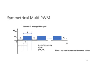
![Symmetrical Multi-PWM (Cont.): Fourier
137
vab
γ-(δ/2)
γ
δ
For 2 pulse per half cycle: vab(t)= Ʃn=1,3,5,… Vpn sin (nwot)
π
0
2π
γ+(δ/2)
δ
δ δ
=
2
2 ∗ sin =
8
sin sin
2
• Example: if δ= 360 γ= [(180-72)/3] +(36/2) =540
The corresponding fundamental peak
Vp1= (8Vd/ π) sin 540 sin 180= 0.637 Vd
+Vd
-Vd](https://image.slidesharecdn.com/4thpowerpeapps-250317150423-64c6a466/85/4th_power_PE-App-enginering-electricql-pdf-137-320.jpg)


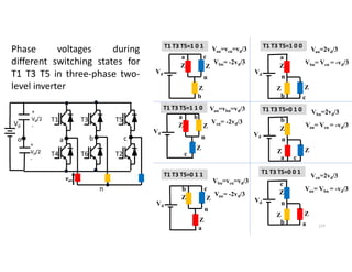
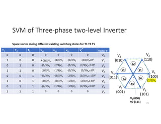
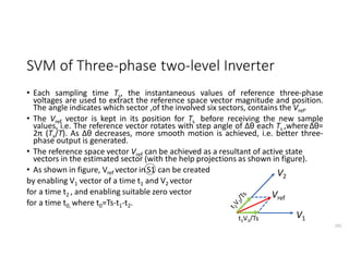
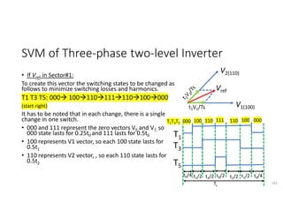
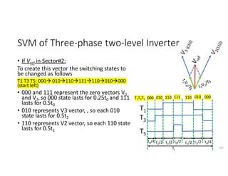
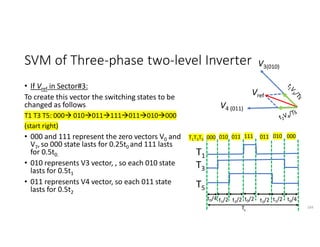
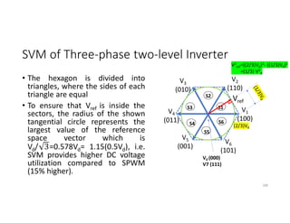
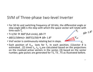
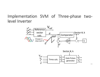
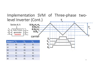
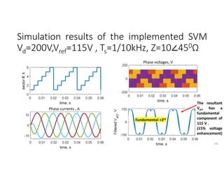
![SVM of Three-phase two-level Inverter
• Any three phase set of variables that add up to zero in the stationary a-b-c
frame can be represented in a complex plane by a complex vector that
contains a real α and imaginary β component.
• Space vector definition of three-phase voltages:
vs = (2/3)[va ej0+ vb ej(2π/3)+ vc ej(4π/3)]
• Space vector represents three phase quantities as a single rotating vector
where the three phases are assumed as only one quantity.
• For the balanced three-phase voltages, the space vector is continuously
rotating with a speed of (2πf) rad/s, where f is the frequency. So If we
create a rotating space vector via changing switching states of the inverter,
three-phase output voltages will be generated successfully.
176](https://image.slidesharecdn.com/4thpowerpeapps-250317150423-64c6a466/85/4th_power_PE-App-enginering-electricql-pdf-176-320.jpg)