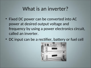
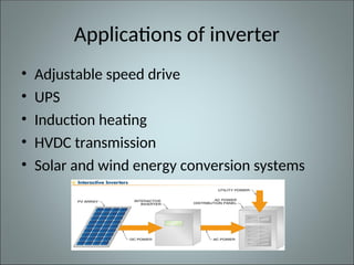
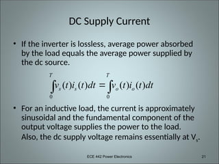
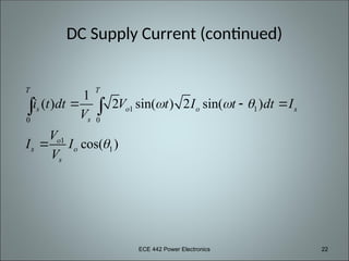
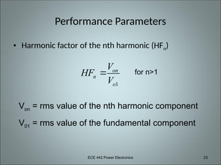
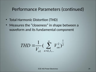
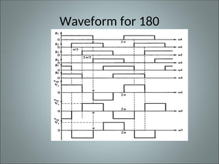
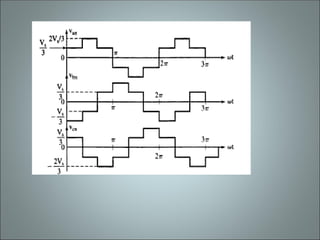
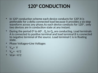
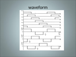
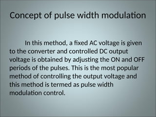
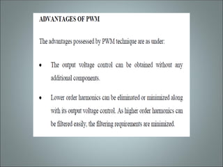
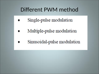
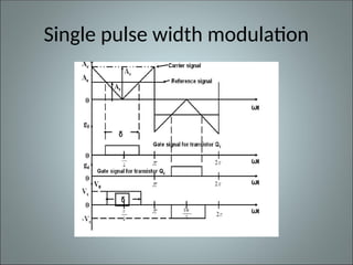
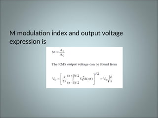
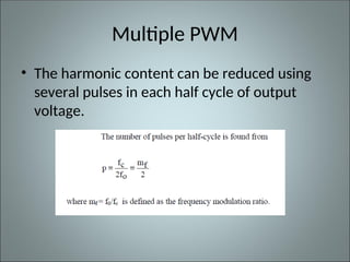
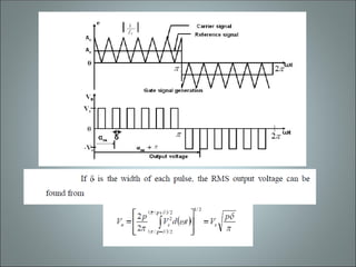
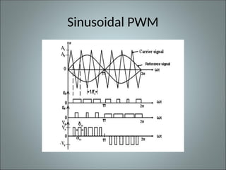
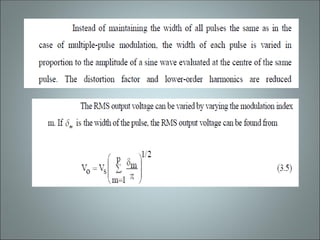
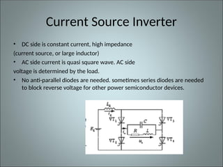
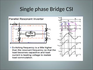
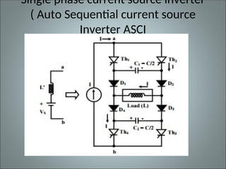
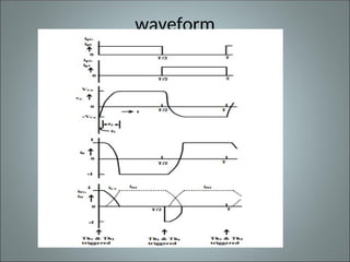
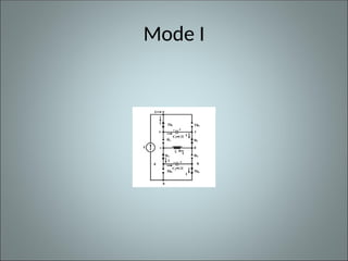
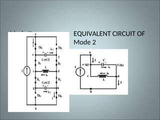
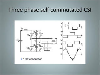
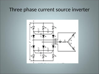
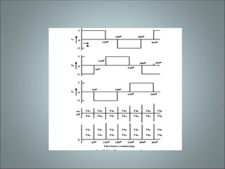
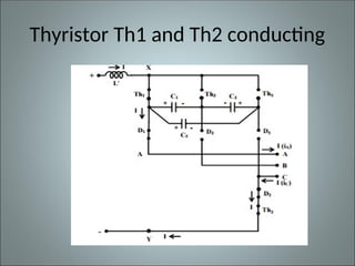
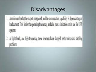
UNIT IV
INVERTERS
What is an inverter?
• Fixed DC power can be converted into AC
power at desired output voltage and
frequency by using a power electronics circuit,
called an inverter.
• DC input can be a rectifier, battery or fuel cell
Applications of inverter
• Adjustable speed drive
• UPS
• Induction heating
• HVDC transmission
• Solar and wind energy conversion systems
Types of inverter
There are two common types of inverters,
• i) Voltage Source Inverters and
•ii) Current Source Inverters.
Single Phase Inverter
Half bridge inverter
Full Bridge Inverter
Three phase inverter
Series and parallel Inverter
Why thyristors are not preferred in
inverter circuit?
The reverse withstanding capability of thyristor
is very less.
Thyristors in inverter circuit requires forced
commutation.
Difference between voltage and
current source inverter
S.No Voltage Source Inverter Current Source Inverter
1. DC source with small resistance
forms fixed dc voltage
DC Source with high resistance forms
fixed dc current
2. Large value of capacitor connected
across the source to maintain
constant voltage
Large value of inductor connected in
series with the source to maintain
constant current
3. Any change in load voltage does
not affect the source voltage
Any change in load current does not
affect the source current
ECE 442 Power Electronics 7
Single-phase half-bridge inverter
ECE 442 Power Electronics 8
Operational Details
• Consists of 2 choppers, 3-wire DC source
• Transistors switched on and off alternately
• Need to isolate the gate signal for Q1 (upper device)
• Each provides opposite polarity of Vs/2 across the load
3-wire DC source
ECE 442 Power Electronics 9
Q1 on, Q2 off, vo = Vs/2
Peak Reverse Voltage of Q2 = Vs
ECE 442 Power Electronics 10
Q1 off, Q2 on, vo = -Vs/2
ECE 442 Power Electronics 11
Waveforms with resistive load
ECE 442 Power Electronics 12
Look at the output voltage
1
2
2
2
0
2
4 2
o
T
s s
o
o
V V
V dt
T
 
 
 
 
 
 

rms value of the output voltage, Vo
ECE 442 Power Electronics 13
Fourier Series of the instantaneous output
voltage
 
1
0
0
1,3,5,..
cos( ) sin( )
2
, 0
1
sin( ) ( ) sin( ) ( )
2 2
2
1,3,5,...
2
sin( )
o
o n n
n
o n
s s
n
s
n
s
o
n
a
v a n t b n t
a a
V V
b n t d t n t d t
V
b n
n
V
v n t
n


 
   









  

 

 
 
 
  


 

ECE 442 Power Electronics 14
rms value of the fundamental component
1,3,5,..
1
1
2
sin
2
1
2
0.45
s
o
n
s
o
o s
V
v n t
n
V
V
V V









ECE 442 Power Electronics 15
When the load is highly inductive
ECE 442 Power Electronics 16
Turn off Q1 at t = To/2
Current falls to 0 via D2, L, Vs/2 lower
+
Vs/2
-
+
Vs/2
-
ECE 442 Power Electronics 17
Turn off Q2 at t = To
Current falls to 0 via D1, L, Vs/2 upper
+
Vs/2
-
+
Vs/2
-
ECE 442 Power Electronics 18
Load Current for a highly inductive load
Transistors are only switched on for a quarter-cycle, or 90
ECE 442 Power Electronics 19
Fourier Series of the output current for an RL
load
2 2
1,3,5,...
1
2
sin( )
( )
tan ( )
o o s
o n
n
n
v v V
i n t
Z R jn L n R n L
n L
R
 
  





   
 


ECE 442 Power Electronics 20
Fundamental Output Power
In most cases, the useful power
2
1 1 1 1 1
2
1 2 2
cos
2
2 ( )
o o o o
s
o
P V I I R
V
P R
R L

 
 
 
 
  
 
ECE 442 Power Electronics 21
DC Supply Current
• If the inverter is lossless, average power absorbed
by the load equals the average power supplied by
the dc source.
• For an inductive load, the current is approximately
sinusoidal and the fundamental component of the
output voltage supplies the power to the load.
Also, the dc supply voltage remains essentially at Vs.
0 0
( ) ( ) ( ) ( )
T T
s s o o
v t i t dt v t i t dt

 
ECE 442 Power Electronics 22
1 1
0 0
1
1
1
( ) 2 sin( ) 2 sin( )
cos( )
T T
s o o s
s
o
s o
s
i t dt V t I t dt I
V
V
I I
V
  

  

 
DC Supply Current (continued)
ECE 442 Power Electronics 23
Performance Parameters
• Harmonic factor of the nth harmonic (HFn)
1
on
n
o
V
HF
V
 for n>1
Von = rms value of the nth harmonic component
V01 = rms value of the fundamental component
ECE 442 Power Electronics 24
Performance Parameters (continued)
• Total Harmonic Distortion (THD)
• Measures the “closeness” in shape between a
waveform and its fundamental component
1
2 2
2,3,...
1
1
( )
on
n
o
THD V
V


 
ECE 442 Power Electronics 25
Performance Parameters (continued)
• Distortion Factor (DF)
• Indicates the amount of HD that remains in a
particular waveform after the harmonics have been
subjected to second-order attenuation.
1
2 2
2
2,3,...
1
2
1
1 on
n
o
on
n
o
V
DF
V n
V
DF
V n


 
 
  
 
 
 
 


for n>1
ECE 442 Power Electronics 26
Performance Parameters (continued)
• Lowest order harmonic (LOH)
• The harmonic component whose frequency is
closest to the fundamental, and its amplitude
is greater than or equal to 3% of the
amplitude of the fundamental component.
ECE 442 Power Electronics 27
Single-phase full-bridge inverter
ECE 442 Power Electronics 28
Operational Details
• Consists of 4 choppers and a 3-wire DC source
• Q1-Q2 and Q3-Q4 switched on and off alternately
• Need to isolate the gate signal for Q1 and Q3 (upper)
• Each pair provide opposite polarity of Vsacross the load
ECE 442 Power Electronics 29
Q1-Q2 on, Q3-Q4 off, vo = Vs
+ Vs -
ECE 442 Power Electronics 30
Q3-Q4 on, Q1-Q2 off, vo = -Vs
- Vs +
ECE 442 Power Electronics 31
When the load is highly inductive
Turn Q1-Q2 off – Q3-Q4 off
ECE 442 Power Electronics 32
Turn Q3-Q4 off – Q1-Q2 off
ECE 442 Power Electronics 33
Load current for a highly inductive load
Three Phase Bridge Inverter
180 degree mode of operation
• In 1800
conduction scheme,each device
conducts for 1800
. They are turned ON at
regular interval of 600
in the sequence
Q1,Q2,Q3,Q4,Q5,Q6.The output terminals A B and
C of this bridge are connected to the terminals
of a 3-phase star or delta connected load.
Hence, load voltages are
VAN=V/3,
VBN=-2V/3,
VCN=V/3
Line volages are
VAB=VAN-VBN=V,
VBC=VBN-VCN=-V ,
VCA=VCN-VAN=0
Waveform for 180
1200
CONDUCTION
• In 1200
conduction scheme each device conducts for 1200
.It is
preferable for a delta connected load because it provides a six step
waveform across any phase.As each device conducts for 1200 , only
two devices are in conduction state at any instant.
• During the period 00
to 600
, Q1 to Q6 are conducting. Load terminals
A is connected to positive terminal and load terminal B is connected
to negative terminal of the source. Load terminal C is in floating
state.
• Phase Voltages=Line Voltages
• VAB= V
• VBC= -V/2
• Vca= -V/2
Equivalent circuit
waveform
Concept of pulse width modulation
In this method, a fixed AC voltage is given
to the converter and controlled DC output
voltage is obtained by adjusting the ON and OFF
periods of the pulses. This is the most popular
method of controlling the output voltage and
this method is termed as pulse width
modulation control.
Different PWM method
Single pulse width modulation
M modulation index and output voltage
expression is
Multiple PWM
• The harmonic content can be reduced using
several pulses in each half cycle of output
voltage.
Sinusoidal PWM
Current Source Inverter
• DC side is constant current, high impedance
(current source, or large inductor)
• AC side current is quasi square wave. AC side
voltage is determined by the load.
• No anti-parallel diodes are needed. sometimes series diodes are needed
to block reverse voltage for other power semiconductor devices.
Single phase Bridge CSI
Single phase current source inverter
( Auto Sequential current source
Inverter ASCI
0
waveform
Mode I
Mode II EQUIVALENT CIRCUIT OF
Mode 2
Three phase self commutated CSI
Three phase current source inverter
Thyristor Th1 and Th2 conducting
Mode I
Mode 2
Th3 and Th2 Conduction
Advantages
Disadvantages

power electronics engineering UNIT IV.ppt

  • 1.
  • 2.
    What is aninverter? • Fixed DC power can be converted into AC power at desired output voltage and frequency by using a power electronics circuit, called an inverter. • DC input can be a rectifier, battery or fuel cell
  • 3.
    Applications of inverter •Adjustable speed drive • UPS • Induction heating • HVDC transmission • Solar and wind energy conversion systems
  • 4.
    Types of inverter Thereare two common types of inverters, • i) Voltage Source Inverters and •ii) Current Source Inverters. Single Phase Inverter Half bridge inverter Full Bridge Inverter Three phase inverter Series and parallel Inverter
  • 5.
    Why thyristors arenot preferred in inverter circuit? The reverse withstanding capability of thyristor is very less. Thyristors in inverter circuit requires forced commutation.
  • 6.
    Difference between voltageand current source inverter S.No Voltage Source Inverter Current Source Inverter 1. DC source with small resistance forms fixed dc voltage DC Source with high resistance forms fixed dc current 2. Large value of capacitor connected across the source to maintain constant voltage Large value of inductor connected in series with the source to maintain constant current 3. Any change in load voltage does not affect the source voltage Any change in load current does not affect the source current
  • 7.
    ECE 442 PowerElectronics 7 Single-phase half-bridge inverter
  • 8.
    ECE 442 PowerElectronics 8 Operational Details • Consists of 2 choppers, 3-wire DC source • Transistors switched on and off alternately • Need to isolate the gate signal for Q1 (upper device) • Each provides opposite polarity of Vs/2 across the load 3-wire DC source
  • 9.
    ECE 442 PowerElectronics 9 Q1 on, Q2 off, vo = Vs/2 Peak Reverse Voltage of Q2 = Vs
  • 10.
    ECE 442 PowerElectronics 10 Q1 off, Q2 on, vo = -Vs/2
  • 11.
    ECE 442 PowerElectronics 11 Waveforms with resistive load
  • 12.
    ECE 442 PowerElectronics 12 Look at the output voltage 1 2 2 2 0 2 4 2 o T s s o o V V V dt T              rms value of the output voltage, Vo
  • 13.
    ECE 442 PowerElectronics 13 Fourier Series of the instantaneous output voltage   1 0 0 1,3,5,.. cos( ) sin( ) 2 , 0 1 sin( ) ( ) sin( ) ( ) 2 2 2 1,3,5,... 2 sin( ) o o n n n o n s s n s n s o n a v a n t b n t a a V V b n t d t n t d t V b n n V v n t n                                      
  • 14.
    ECE 442 PowerElectronics 14 rms value of the fundamental component 1,3,5,.. 1 1 2 sin 2 1 2 0.45 s o n s o o s V v n t n V V V V         
  • 15.
    ECE 442 PowerElectronics 15 When the load is highly inductive
  • 16.
    ECE 442 PowerElectronics 16 Turn off Q1 at t = To/2 Current falls to 0 via D2, L, Vs/2 lower + Vs/2 - + Vs/2 -
  • 17.
    ECE 442 PowerElectronics 17 Turn off Q2 at t = To Current falls to 0 via D1, L, Vs/2 upper + Vs/2 - + Vs/2 -
  • 18.
    ECE 442 PowerElectronics 18 Load Current for a highly inductive load Transistors are only switched on for a quarter-cycle, or 90
  • 19.
    ECE 442 PowerElectronics 19 Fourier Series of the output current for an RL load 2 2 1,3,5,... 1 2 sin( ) ( ) tan ( ) o o s o n n n v v V i n t Z R jn L n R n L n L R                  
  • 20.
    ECE 442 PowerElectronics 20 Fundamental Output Power In most cases, the useful power 2 1 1 1 1 1 2 1 2 2 cos 2 2 ( ) o o o o s o P V I I R V P R R L              
  • 21.
    ECE 442 PowerElectronics 21 DC Supply Current • If the inverter is lossless, average power absorbed by the load equals the average power supplied by the dc source. • For an inductive load, the current is approximately sinusoidal and the fundamental component of the output voltage supplies the power to the load. Also, the dc supply voltage remains essentially at Vs. 0 0 ( ) ( ) ( ) ( ) T T s s o o v t i t dt v t i t dt   
  • 22.
    ECE 442 PowerElectronics 22 1 1 0 0 1 1 1 ( ) 2 sin( ) 2 sin( ) cos( ) T T s o o s s o s o s i t dt V t I t dt I V V I I V           DC Supply Current (continued)
  • 23.
    ECE 442 PowerElectronics 23 Performance Parameters • Harmonic factor of the nth harmonic (HFn) 1 on n o V HF V  for n>1 Von = rms value of the nth harmonic component V01 = rms value of the fundamental component
  • 24.
    ECE 442 PowerElectronics 24 Performance Parameters (continued) • Total Harmonic Distortion (THD) • Measures the “closeness” in shape between a waveform and its fundamental component 1 2 2 2,3,... 1 1 ( ) on n o THD V V    
  • 25.
    ECE 442 PowerElectronics 25 Performance Parameters (continued) • Distortion Factor (DF) • Indicates the amount of HD that remains in a particular waveform after the harmonics have been subjected to second-order attenuation. 1 2 2 2 2,3,... 1 2 1 1 on n o on n o V DF V n V DF V n                    for n>1
  • 26.
    ECE 442 PowerElectronics 26 Performance Parameters (continued) • Lowest order harmonic (LOH) • The harmonic component whose frequency is closest to the fundamental, and its amplitude is greater than or equal to 3% of the amplitude of the fundamental component.
  • 27.
    ECE 442 PowerElectronics 27 Single-phase full-bridge inverter
  • 28.
    ECE 442 PowerElectronics 28 Operational Details • Consists of 4 choppers and a 3-wire DC source • Q1-Q2 and Q3-Q4 switched on and off alternately • Need to isolate the gate signal for Q1 and Q3 (upper) • Each pair provide opposite polarity of Vsacross the load
  • 29.
    ECE 442 PowerElectronics 29 Q1-Q2 on, Q3-Q4 off, vo = Vs + Vs -
  • 30.
    ECE 442 PowerElectronics 30 Q3-Q4 on, Q1-Q2 off, vo = -Vs - Vs +
  • 31.
    ECE 442 PowerElectronics 31 When the load is highly inductive Turn Q1-Q2 off – Q3-Q4 off
  • 32.
    ECE 442 PowerElectronics 32 Turn Q3-Q4 off – Q1-Q2 off
  • 33.
    ECE 442 PowerElectronics 33 Load current for a highly inductive load
  • 34.
  • 35.
    180 degree modeof operation • In 1800 conduction scheme,each device conducts for 1800 . They are turned ON at regular interval of 600 in the sequence Q1,Q2,Q3,Q4,Q5,Q6.The output terminals A B and C of this bridge are connected to the terminals of a 3-phase star or delta connected load.
  • 36.
    Hence, load voltagesare VAN=V/3, VBN=-2V/3, VCN=V/3 Line volages are VAB=VAN-VBN=V, VBC=VBN-VCN=-V , VCA=VCN-VAN=0
  • 37.
  • 39.
    1200 CONDUCTION • In 1200 conductionscheme each device conducts for 1200 .It is preferable for a delta connected load because it provides a six step waveform across any phase.As each device conducts for 1200 , only two devices are in conduction state at any instant. • During the period 00 to 600 , Q1 to Q6 are conducting. Load terminals A is connected to positive terminal and load terminal B is connected to negative terminal of the source. Load terminal C is in floating state. • Phase Voltages=Line Voltages • VAB= V • VBC= -V/2 • Vca= -V/2
  • 40.
  • 41.
  • 42.
    Concept of pulsewidth modulation In this method, a fixed AC voltage is given to the converter and controlled DC output voltage is obtained by adjusting the ON and OFF periods of the pulses. This is the most popular method of controlling the output voltage and this method is termed as pulse width modulation control.
  • 44.
  • 45.
  • 46.
    M modulation indexand output voltage expression is
  • 47.
    Multiple PWM • Theharmonic content can be reduced using several pulses in each half cycle of output voltage.
  • 49.
  • 51.
    Current Source Inverter •DC side is constant current, high impedance (current source, or large inductor) • AC side current is quasi square wave. AC side voltage is determined by the load. • No anti-parallel diodes are needed. sometimes series diodes are needed to block reverse voltage for other power semiconductor devices.
  • 52.
  • 53.
    Single phase currentsource inverter ( Auto Sequential current source Inverter ASCI 0
  • 54.
  • 55.
  • 56.
    Mode II EQUIVALENTCIRCUIT OF Mode 2
  • 57.
    Three phase selfcommutated CSI
  • 58.
    Three phase currentsource inverter
  • 60.
    Thyristor Th1 andTh2 conducting
  • 61.
  • 62.
  • 63.
    Th3 and Th2Conduction
  • 64.
  • 65.