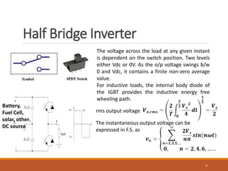
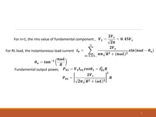
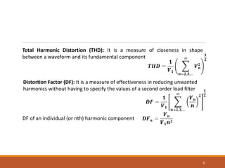
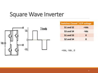
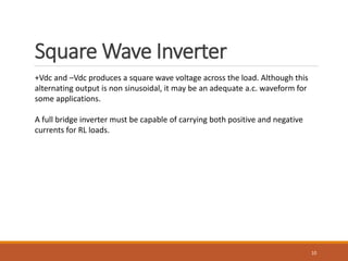
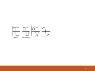
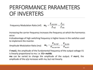
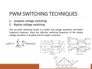
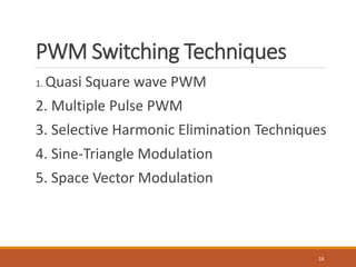
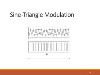
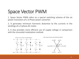
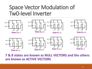
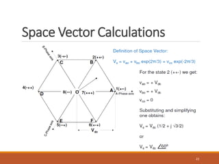
HIGH POWER INVERTERS
TWO LEVEL INVERTERS
NAME : UDAYA BHASKER MANTHATI
DESIGNATION: ASSOCIATE PROFESSOR
DEPARTMENT: ELECTRICAL ENGINEERING
CONTENT
2
Introduction
Principle of Operation
Classification of Inverters
Half Bridge Inverters
Full Bridge Inverters
Applications
3-Ph,2-Level VSI Schemes
PWM switching Techniques
Problems
INTRODUCTION
3
An a.c. output is synthesized from a d.c. input by closing and opening the
switches in an appropriate sequence.
Switching transition times must be accommodated in the control of the
switches. Overlap of switch ‘ON’ times will result in a short circuit, sometimes
called a shoot through fault, across the DC voltage source.
The current waveform in the load depends on the load components. For the
resistive load, the current waveform matches the shape of the output voltage.
An inductive load will have a current that has more of a sinusoidal quality than
the voltage because of the filtering property of the inductance.
Classification of Inverters
4
1. Single phase inverters and 2. Three phase inverters
An inverter is called a voltage fed inverter (VFI) if the input
voltage remains constant.
A current fed inverter (CFI) if the input current is
maintained constant.
A variable dc linked inverter if the input voltage is
controllable.
5
Typical 1-ph o/p’s are: i) 220V/380V at 50Hz
ii) 120V/208V at 60Hz
iii) 115V/200V at 400Hz
Inverters use PWM control signals for producing an AC output voltage.
Low and medium power applications, square wave or quasi square
wave voltage may be acceptable. For high power applications, low
distorted sinusoidal waveforms are required.
Applications: 1. Adjustable speed a.c. motor drives.
2.Uninterruptable power supplies,
3. Induction heating.
4. Running A.C. appliances from an automobile battery
5. Electric Vehicles
6. Control and Protection
Half Bridge Inverter
6
The voltage across the load at any given instant
is dependent on the switch position. Two levels
either Vdc or 0V. As the o/p voltage swings b/w
0 and Vdc, it contains a finite non-zero average
value.
For inductive loads, the internal body diode of
the IGBT provides the inductive energy free
wheeling path.
rms output voltage
The instantaneous output voltage can be
expressed in F.S. as
Battery,
Fuel Cell,
solar, other
DC source
7
For n=1, the rms value of fundamental component ,
For RL load, the instantaneous load current
Fundamental output power,
8
Total Harmonic Distortion (THD): It is a measure of closeness in shape
between a waveform and its fundamental component
Distortion Factor (DF): It is a measure of effectiveness in reducing unwanted
harmonics without having to specify the values of a second order load filter
DF of an individual (or nth) harmonic component
Square Wave Inverter
Switches Closed O/P voltage
S1 and S2 +Vdc
S3 and S4 -Vdc
S1 and S3 0
S2 and S4 0
9
+Vdc, -Vdc , 0
Square Wave Inverter
10
+Vdc and –Vdc produces a square wave voltage across the load. Although this
alternating output is non sinusoidal, it may be an adequate a.c. waveform for
some applications.
A full bridge inverter must be capable of carrying both positive and negative
currents for RL loads.
11
PERFORMANCE PARAMETERS
OF INVERTERS
12
Frequency Modulation Ratio (mf)
Increasing the carrier frequency increases the frequency at which the harmonics
occur.
A disadvantage of high switching frequency is higher losses in the switches used
to implement the inverter.
Amplitude Modulation Ratio (ma)
If ma≤1, the amplitude of the fundamental frequency of the output voltage V1
is linearly proportional to ma. i.e. V1= maVdc
ma can be varied to change the amplitude of the output. If ma>1, the
amplitude of the o/p increases with ma, but not linearly.
PWM SWITCHING TECHNIQUES
13
1. Unipolar voltage switching
2. Bipolar voltage switching
The uni polar switching results in a better o/p voltage waveform and better
frequency response. Since the effective switching frequency of the output
voltage waveform is doubled and the ripple is reduced.
Uni polar Switching
14
The triangular carrier waveform is compared with two reference
signals which are positive and negative signal.
Bipolar Switching
15
16
Unipolar voltage switching scheme has better harmonic profile
compare to bipolar voltage switching.
The output is switched either from high to zero and low to zero,
rather than between high and low as in bipolar switching
3-PHASE, 2-LEVEL VOLTAGE
SOURCE INVERTERS
Objectives of PWM Techniques:
1. One must be able to exercise control over the magnitude and
frequency of the fundamental component to suit the control objectives.
2. The spectral performance (THD) should be acceptable.
3. Good utilization of DC supplies voltage possibly a high voltage gain.
17
PWM Switching Techniques
1. Quasi Square wave PWM
2. Multiple Pulse PWM
3. Selective Harmonic Elimination Techniques
4. Sine-Triangle Modulation
5. Space Vector Modulation
18
Sine-Triangle Modulation
19
Space Vector PWM
1. Space Vector PWM refers to a special switching scheme of the six
power transistors of a 3-Phase power converter.
2. It generates minimum harmonic distortion to the currents in the
windings of a 3-phase AC motor.
3. It also provides more efficient use of supply voltage in comparison
with the sinusoidal modulation method.
20
Space Vector Modulation of
Tw0-level Inverter
7 & 8 states are known as NULL VECTORS and the others
are known as ACTIVE VECTORS
21
Space Vector Calculations
22
Advantages of Space Vector
Modulation
1. The switching is automatic
2. No need of sector identification.
3.Depends only on the magnitudes of
instantaneous three phase reference voltages.
23
24
A single phase half bridge inverter has a resistive
load of R =2.4 Ohm and DC input voltage is 48V.
Determine a) the rms output voltage at the
fundamental frequency b) the output power c)
the average and peak currents of each transistor
d) the peak reverse blocking voltage of each
transistor d) the total THD f) Distortion Factor
25
The full-bridge inverter is used to produce a 60Hz voltage across a
series RL load using bipolar PWM. The dc input to the bridge is
100V, the amplitude modulation ration is 0.8 and the frequency
modulation ratio is 21. The load has a resistance of R= 100Ohm and
series inductance L =20mH. Determine a) the amplitude of the 60Hz
component of the output voltage and load current b) the power
absorbed by the load resistor and c) the THD of the load current.
ma= 1 0.9 0.8 0.7 0.6 0.5 0.4 0.3 0.2 0.1
n = 1 1 0.9 0.8 0.7 0.6 0.5 0.4 0.3 0.2 0.1
n = mf 0.6 0.71 0.82 0.92 1.01 1.08 1.15 1.2 1.24 1.27
n = mf
±2
0.32 0.27 0.22 0.17 0.13 0.09 0.06 0.03 0.02 0
Fourierco-efficients(Vn/VDC)areas follows:
THANK YOU
26

High power Inverters Introduction & Applications

  • 1.
    HIGH POWER INVERTERS TWOLEVEL INVERTERS NAME : UDAYA BHASKER MANTHATI DESIGNATION: ASSOCIATE PROFESSOR DEPARTMENT: ELECTRICAL ENGINEERING
  • 2.
    CONTENT 2 Introduction Principle of Operation Classificationof Inverters Half Bridge Inverters Full Bridge Inverters Applications 3-Ph,2-Level VSI Schemes PWM switching Techniques Problems
  • 3.
    INTRODUCTION 3 An a.c. outputis synthesized from a d.c. input by closing and opening the switches in an appropriate sequence. Switching transition times must be accommodated in the control of the switches. Overlap of switch ‘ON’ times will result in a short circuit, sometimes called a shoot through fault, across the DC voltage source. The current waveform in the load depends on the load components. For the resistive load, the current waveform matches the shape of the output voltage. An inductive load will have a current that has more of a sinusoidal quality than the voltage because of the filtering property of the inductance.
  • 4.
    Classification of Inverters 4 1.Single phase inverters and 2. Three phase inverters An inverter is called a voltage fed inverter (VFI) if the input voltage remains constant. A current fed inverter (CFI) if the input current is maintained constant. A variable dc linked inverter if the input voltage is controllable.
  • 5.
    5 Typical 1-ph o/p’sare: i) 220V/380V at 50Hz ii) 120V/208V at 60Hz iii) 115V/200V at 400Hz Inverters use PWM control signals for producing an AC output voltage. Low and medium power applications, square wave or quasi square wave voltage may be acceptable. For high power applications, low distorted sinusoidal waveforms are required. Applications: 1. Adjustable speed a.c. motor drives. 2.Uninterruptable power supplies, 3. Induction heating. 4. Running A.C. appliances from an automobile battery 5. Electric Vehicles 6. Control and Protection
  • 6.
    Half Bridge Inverter 6 Thevoltage across the load at any given instant is dependent on the switch position. Two levels either Vdc or 0V. As the o/p voltage swings b/w 0 and Vdc, it contains a finite non-zero average value. For inductive loads, the internal body diode of the IGBT provides the inductive energy free wheeling path. rms output voltage The instantaneous output voltage can be expressed in F.S. as Battery, Fuel Cell, solar, other DC source
  • 7.
    7 For n=1, therms value of fundamental component , For RL load, the instantaneous load current Fundamental output power,
  • 8.
    8 Total Harmonic Distortion(THD): It is a measure of closeness in shape between a waveform and its fundamental component Distortion Factor (DF): It is a measure of effectiveness in reducing unwanted harmonics without having to specify the values of a second order load filter DF of an individual (or nth) harmonic component
  • 9.
    Square Wave Inverter SwitchesClosed O/P voltage S1 and S2 +Vdc S3 and S4 -Vdc S1 and S3 0 S2 and S4 0 9 +Vdc, -Vdc , 0
  • 10.
    Square Wave Inverter 10 +Vdcand –Vdc produces a square wave voltage across the load. Although this alternating output is non sinusoidal, it may be an adequate a.c. waveform for some applications. A full bridge inverter must be capable of carrying both positive and negative currents for RL loads.
  • 11.
  • 12.
    PERFORMANCE PARAMETERS OF INVERTERS 12 FrequencyModulation Ratio (mf) Increasing the carrier frequency increases the frequency at which the harmonics occur. A disadvantage of high switching frequency is higher losses in the switches used to implement the inverter. Amplitude Modulation Ratio (ma) If ma≤1, the amplitude of the fundamental frequency of the output voltage V1 is linearly proportional to ma. i.e. V1= maVdc ma can be varied to change the amplitude of the output. If ma>1, the amplitude of the o/p increases with ma, but not linearly.
  • 13.
    PWM SWITCHING TECHNIQUES 13 1.Unipolar voltage switching 2. Bipolar voltage switching The uni polar switching results in a better o/p voltage waveform and better frequency response. Since the effective switching frequency of the output voltage waveform is doubled and the ripple is reduced.
  • 14.
    Uni polar Switching 14 Thetriangular carrier waveform is compared with two reference signals which are positive and negative signal.
  • 15.
  • 16.
    16 Unipolar voltage switchingscheme has better harmonic profile compare to bipolar voltage switching. The output is switched either from high to zero and low to zero, rather than between high and low as in bipolar switching
  • 17.
    3-PHASE, 2-LEVEL VOLTAGE SOURCEINVERTERS Objectives of PWM Techniques: 1. One must be able to exercise control over the magnitude and frequency of the fundamental component to suit the control objectives. 2. The spectral performance (THD) should be acceptable. 3. Good utilization of DC supplies voltage possibly a high voltage gain. 17
  • 18.
    PWM Switching Techniques 1.Quasi Square wave PWM 2. Multiple Pulse PWM 3. Selective Harmonic Elimination Techniques 4. Sine-Triangle Modulation 5. Space Vector Modulation 18
  • 19.
  • 20.
    Space Vector PWM 1.Space Vector PWM refers to a special switching scheme of the six power transistors of a 3-Phase power converter. 2. It generates minimum harmonic distortion to the currents in the windings of a 3-phase AC motor. 3. It also provides more efficient use of supply voltage in comparison with the sinusoidal modulation method. 20
  • 21.
    Space Vector Modulationof Tw0-level Inverter 7 & 8 states are known as NULL VECTORS and the others are known as ACTIVE VECTORS 21
  • 22.
  • 23.
    Advantages of SpaceVector Modulation 1. The switching is automatic 2. No need of sector identification. 3.Depends only on the magnitudes of instantaneous three phase reference voltages. 23
  • 24.
    24 A single phasehalf bridge inverter has a resistive load of R =2.4 Ohm and DC input voltage is 48V. Determine a) the rms output voltage at the fundamental frequency b) the output power c) the average and peak currents of each transistor d) the peak reverse blocking voltage of each transistor d) the total THD f) Distortion Factor
  • 25.
    25 The full-bridge inverteris used to produce a 60Hz voltage across a series RL load using bipolar PWM. The dc input to the bridge is 100V, the amplitude modulation ration is 0.8 and the frequency modulation ratio is 21. The load has a resistance of R= 100Ohm and series inductance L =20mH. Determine a) the amplitude of the 60Hz component of the output voltage and load current b) the power absorbed by the load resistor and c) the THD of the load current. ma= 1 0.9 0.8 0.7 0.6 0.5 0.4 0.3 0.2 0.1 n = 1 1 0.9 0.8 0.7 0.6 0.5 0.4 0.3 0.2 0.1 n = mf 0.6 0.71 0.82 0.92 1.01 1.08 1.15 1.2 1.24 1.27 n = mf ±2 0.32 0.27 0.22 0.17 0.13 0.09 0.06 0.03 0.02 0 Fourierco-efficients(Vn/VDC)areas follows:
  • 26.