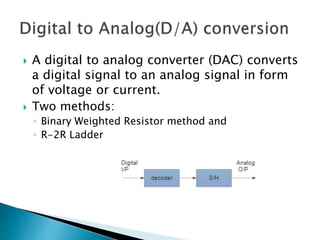
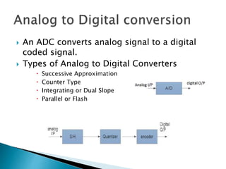
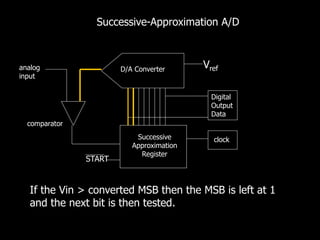
Done by,
S.PRAVEENKUMAR.
 A digital to analog converter (DAC) converts
a digital signal to an analog signal in form
of voltage or current.
 Two methods:
◦ Binary Weighted Resistor method and
◦ R-2R Ladder
 Depending upon the digital input bit Logic
circuit performs switching of resistor
networks between Vref and ground.
 Transistors are used to switch between Vref
and ground (bit high or low)
 weighted resistors are used to distinguish
each bit from the MSB to LSB.
Resistors are connected to Vref if
corresponding bit is high or
ground if corresponding bit is
low
The output voltage is,
rf1-n
1-n210
ffo
242
ER
R
a
R
a
R
a
R
a
RIE 





 
ffo RIE 
R
RE
E fr
o 
If R is connected to Er,
For a code of 1001
The general expression is,
 Advantages
◦ Simple Construction/Analysis
◦ Fast Conversion
 Disadvantages
◦ A 10 bit DAC needs resistors ranging from R to
R/1024.
◦ Requires low switch resistances in transistors
◦ Can be expensive. Therefore, usually limited
to 8-bit resolution.
 An ADC converts analog signal to a digital
coded signal.
 Types of Analog to Digital Converters
 Successive Approximation
 Counter Type
 Integrating or Dual Slope
 Parallel or Flash
 Sampling - the analog signal is first sampled
at periodic intervals.
 Quantizing - breaking down analog value into
a set of finite states
 Encoding - assigning a digital word or
number to each state and matching it to the
input signal
Successive Approximation method
Successive
Approximation
Register
D/A Converter Vref
clock
analog
input
Digital
Output
Data
At initialization, all bits from the SAR are set to
zero(clearing), and conversion begins by taking START
line low.
comparator
START
+ -
Successive
Approximation
Register
D/A Converter Vref
clock
analog
input
Digital
Output
Data
comparator
START
Successive-Approximation A/D
First the logic circuit in the SAR sets the MSB bit
equal to 1 (+5 V). The MSB representing one half
of full scale is converted by D/A converter.
Successive
Approximation
Register
D/A Converter Vref
clock
analog
input
Digital
Output
Data
comparator
START
Successive-Approximation A/D
If the Vin > converted MSB then the MSB is left at 1
and the next bit is then tested.
Successive
Approximation
Register
D/A Converter Vref
clock
analog
input
Digital
Output
Data
comparator
START
Successive-Approximation A/D
If the Vin < converted MSB then the MSB is left at 1
and the next bit is then tested.
CLOCK PERIOD
¼FS
½FS
¾FS
1 2 3 4 5 6 7 8
analog input
voltage(Vin)
D/A output for 8-bit
conversion with output
code 1011 0101
Advantages
 Medium accuracy compared to
other ADC types
 Capable of outputting the binary
number in serial (one bit at a time)
format.
 increasing the resolution which
improves the accuracy
 increasing the sampling time
which increases the maximum
frequency that can be
measured.
Disadvantages
 Higher resolution successive
approximation ADC’s will be
slower
 Speed limited to ~5Msps

(D/A) and (A/D)conversion