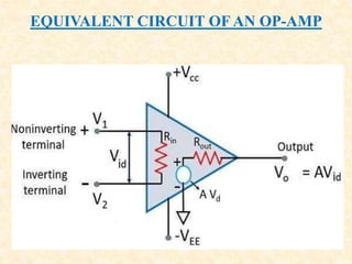
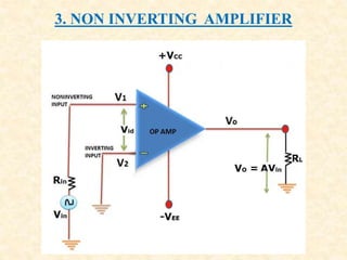
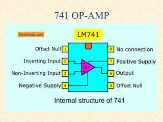
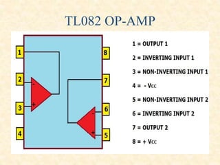
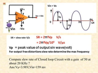
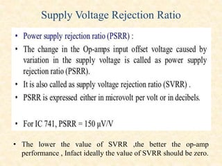
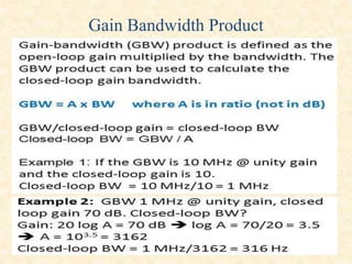
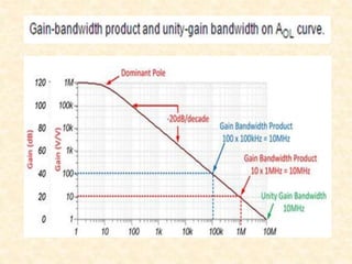
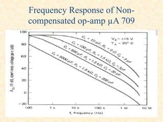
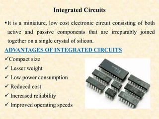
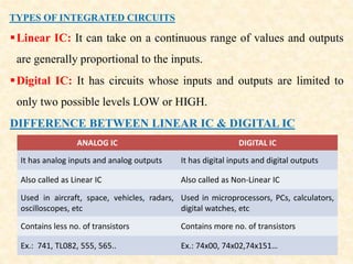
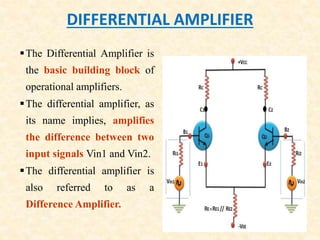
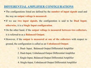
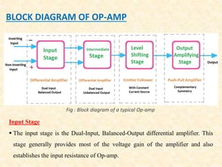
SlideShare a Scribd company logo
INTEGRATED CIRCUITS
AND APPLICATIONS
UNIT-I
OPERATIONALAMPLIFIER
Integrated Circuits
It is a miniature, low cost electronic circuit consisting of both
active and passive components that are irreparably joined
together on a single crystal of silicon.
ADVANTAGES OF INTEGRATED CIRCUITS
Compact size
 Lesser weight
 Low power consumption
 Reduced cost
 Increased reliability
 Improved operating speeds
TYPES OF INTEGRATED CIRCUITS
Linear IC: It can take on a continuous range of values and outputs
are generally proportional to the inputs.
Digital IC: It has circuits whose inputs and outputs are limited to
only two possible levels LOW or HIGH.
DIFFERENCE BETWEEN LINEAR IC & DIGITAL IC
ANALOG IC DIGITAL IC
It has analog inputs and analog outputs It has digital inputs and digital outputs
Also called as Linear IC Also called as Non-Linear IC
Used in aircraft, space, vehicles, radars,
oscilloscopes, etc
Used in microprocessors, PCs, calculators,
digital watches, etc
Contains less no. of transistors Contains more no. of transistors
Ex.: 741, TL082, 555, 565.. Ex.: 74x00, 74x02,74x151…
• Digital IC’s are used to form circuits such as Gates,
Counters, Multiplexers, De multiplexers ,shift registers
and others..,
• Linear IC’s are used to form circuits such as amplifiers,
filters, frequency multipliers and modulators that often
require additional components for satisfactory operation.
Also referred as analog circuits.
• OP-Amps are again classified as
• General purpose: used for variety of applications such as
Integrator , Differentiator, summing amplifier etc.., Ex:
741 IC
• Special purpose: used for the specific applications they
are designed.Ex:LM380 can be used only for audio
applications
• Integrated circuits may be classified as either Monolithic
or Hybrid.
• Most linear IC’s are produced by the monolithic process
in that all transistors and passive elements are fabricated
on a single piece of semiconductor material usually
silicon.
• In Hybrid IC’s passive components and the
interconnections between them are formed on an
insulating substrate. Active components as well as
Monolithic IC’s are then connected to form a complete
circuit.
IC MANUFACTURING COMPANIES
COMPANY SERIES
Fair child μA, μAF
Motorola MC, MFC
Burrbrown BB
Signetics N/S, NE/SE
Texas Instruments SN
National Semiconductor LH, LM, LF
RCA CA, CD
• IC’s are classified according to number of
components as
Introduction
• An operational Amplifier(Op-Amp) is a direct-coupled
high gain amplifier usually followed by a level translator
and an output stage.
• The Op-Amp is a versatile device that can be used to
amplify DC as well as AC input signals and was originally
designed for performing mathematical operations such as
addition, subtraction, multiplication and integration.
• With the addition of suitable external feedback
components, the modern day op-amp can be used for a
variety of applications such as AC & DC signal
amplification , active filters, oscillators, comparators,
regulators etc..,
DIFFERENTIAL AMPLIFIER
The Differential Amplifier is
the basic building block of
operational amplifiers.
The differential amplifier, as
its name implies, amplifies
the difference between two
input signals Vin1 and Vin2.
The differential amplifier is
also referred to as a
Difference Amplifier.
DIFFERENTIAL AMPLIFIER CONFIGURATIONS
 The configurations listed are defined by the number of input signals used and
the way an output voltage is measured.
 If we use two input signals, the configuration is said to be Dual Input;
otherwise, it is a Single Input configuration.
 On the other hand, if the output voltage is measured between two collectors,
it is referred to as a Balanced Output.
 However, if the output is measured at one of the collectors with respect to
ground, the configuration is called as an Unbalanced Output.
1. Dual- Input, Balanced Output Differential Amplifier
2. Dual-Input, Unbalanced Output Differential Amplifier
3. Single-Input, Balanced Output Differential Amplifier
4. Single-Input, Unbalanced Output Differential Amplifier
BLOCK DIAGRAM OF OP-AMP
Fig : Block diagram of a typical Op-amp
Input Stage
 The input stage is the Dual-Input, Balanced-Output differential amplifier. This
stage generally provides most of the voltage gain of the amplifier and also
establishes the input resistance of Op-amp.
Intermediate Stage
 The intermediate stage is Dual-Input, Unbalanced (Single-Ended) Output.
Because direct coupling is used, the DC voltage at the output of the intermediate
stage is well above ground potential.
Level Shifting Stage
 The level translator (Shifting) circuit is used after the intermediate stage to shift
the DC level at the output of the intermediate stage downward to zero volts with
respect to ground.
Output Stage
 The final stage is usually a push pull complementary amplifier output stage; it
increases the output voltage swing and raises the current supplying capability of
the Op-amp. A well designed output stage also provides low output resistance.
CURRENT MIRROR (or) CONSTANT CURRENT
SOURCE
A constant current source makes use of
fact that for a transistor in the active
mode of operation, the collector
current is relatively independent of
collector voltage.
 Since both transistors are matched
their collector currents and base
currents are equal,
i.e. IC1 = IC2 and IB1 = IB2
 Since ‘β’ is very large value,
IREF = IC2 and
LEVEL TRANSLATOR
In the cascade arrangement because of direct coupling no
coupling capacitors are used. Therefore, the DC voltage at the
output terminals tends to rise above the ground.
If several amplifiers are cascaded, the effect is cumulative. This
affects the output voltage swing and causes amplitude
distortion.
This is not desirable; therefore the DC level is brought down to
ground level (i.e., Zero) by means of a level translator.
Basically the level translator is an emitter follower(Common
Collector Amplifier). A simple level translator is shown in
figure.
CIRCUIT SYMBOL OF AN OPEARTIONALAMPLIFIER
 The circuit symbol of an Op-Amp is a triangular as shown in figure.
 It has two input terminals and one output terminal.
 The +VCC and –VEE power supply terminals are connected to two DC Voltage
sources.
• *Estimate ICQ, VCEQ, re, voltage gain, input and output resistances
for a dual-input, balanced-output differential amplifier with circuit
parameters RC = 2.2 kΩ, RE = 4.7 kΩ, Rin1 = Rin2 = 50 Ω,
VCC = +10 V, ‫׀‬-VEE‫׀‬ = 10 V, 𝛽𝐷𝐶 = 𝛽𝐴𝐶 = 100 and 𝑉𝐵𝐸 = 0.71V.
• Solution: ICQ=IE =[(VEE-VBE)/(2RE+Rin/β)]
– ICQ=IE =[10-0.71]/[2*4700+(50/100)] = 0.988mA
• VCEQ = VCE = VCC + VBE - ICQ RC
• VCEQ = VCE =10 + 0.71- 0.988*10-3 = 8.53V
• The ac emitter resistance re=VT/IE=25mV/IE =25mV/0.988mA =
25.3 Ω
• Voltage Gain Ad=Vo/Vid=RC/re =2200/25.3 = 86.96
• Input Resistance Ri=2βac re =2*100*25.3 = 5.06KΩ
• Output Resistance Ro =RC = 2.2KΩ
• *A dual input, unbalanced-output differential amplifier has
the following specification: |Vcc| = 10 V,|-VEE| = 10 V, Rc1 =
Rc2 = 2.7 kΩ, Rin = 50 Ω and RE = 3.9 kΩ and the transistor
is CA3086 with βac = βdc = 100 and VBE = 0.715 V.
Calculate: (i) ICQ and VCEQ values. (ii) Voltage gain. (iii)
Input and output resistances.
• Solution: ICQ=IE =[(VEE-VBE)/(2RE+Rin/β)]
– ICQ=IE =[10-0.71]/[2*3900+(50/100)] = 1.19mA
• VCEQ = VCE = VCC + VBE - ICQ RC
• VCEQ = VCE =10 + 0.71 - 1.19*10-3 = 7.502V
• The ac emitter resistance re=VT/IE=25mV/IE
=25mV/1.19mA = 21 Ω
• Voltage Gain Ad=Vo/Vid=RC/2re =2700/(2*21) = 64.28
• Input Resistance Ri=2βac re =2*100*21 = 4.2KΩ
• Output Resistance Ro =RC = 2.7KΩ
THE IDEAL OP-AMP
 An Ideal Op-amp would exhibit the following electrical characteristics:
1. Infinite open loop voltage gain (AOL = ∞).
2. Infinite input resistance (Ri) so that almost any signal source can drive it
and there is no loading of the preceding stage (Ri = ∞).
3. Zero output resistance (RO) so that output can drive an infinite number of
other devices (RO = 0).
4. Zero output voltage when input voltage is zero.(Zero offset i.e. VO = 0
when V1 = V2 =0).
5. Infinite bandwidth so that any frequency signal from 0 to ∞ Hz can be
amplified without attenuation (BW = ∞).
6. Infinite Common-mode rejection ratio so that the output common-mode
noise voltage is zero (CMMR= ∞).
7. Infinite slew rate so that output voltage changes occur simultaneously with
input voltage changes (SR= ∞).
EQUIVALENT CIRCUIT OF AN OP-AMP
EQUIVALENT CIRCUIT OF AN OP-AMP (CONT…)
 The equivalent circuit is useful in analyzing the basic operating principles of
Op-amps and in observing the effects of feedback arrangements.
• Output voltage, VO = A Vid
VO = A (V1- V2) ---------①
Where A=Large Signal Voltage Gain
Vid=Difference input voltage
V1=Voltage at the Non-Inverting terminal wrt to Ground.
V2=Voltage at the Inverting terminal wrt to Ground.
 Equation ① indicates that the output voltage VO is directly proportional to
the algebraic difference between the two input voltages.
 In other words, the Op-amp amplifies the difference between the two input
voltages; it does not amplify the input voltages themselves. For this reason
the polarity of the output voltage depends on the polarity of the difference
voltage.
OPEN-LOOP OP-AMP CONFIGURATIONS
 In the case of amplifiers the term open loop indicates that, the output
signal is not feedback in any form as part of the input signal and the
loop that would have been formed with feedback is open.
 When connected in open-loop connection, the Op-amp simply
functions as a high-gain amplifier.
 There are three open-loop Op-amp configurations:
1. Differential Amplifier
2. Inverting Amplifier
3. Non Inverting Amplifier
 These configurations are classified according to the number of inputs
used and the terminal to which the input is applied when single input
is used.
1. THE DIFFERENTIALAMPLIFIER
THE DIFFERENTIAL AMPLIFIER (CONT…)
Figure shows the open-loop differential amplifier in which input
signals Vin1 and Vin2 are applied to the positive and negative
input terminals.
Since the Op-amp amplifies the difference between the two
input signals, this configuration is called the differential
amplifier.
The source resistances Rin1 and Rin2 are normally negligible
compared to the input resistance Ri.
Therefore, the voltage drops across these resistors can be
assumed to be zero, which implies that V1 = Vin1 and Vin2.
VO = A (Vin1 - Vin2)
2. INVERTING AMPLIFIER
2. INVERTING AMPLIFIER(Contd..,)
In the Inverting Amplifier only one input is applied and that is
to the inverting input terminal. The Non Inverting input terminal
is grounded.
– Here, V1 = 0 and V2 = Vin
– The basic Op-amp equation,
– VO = AVid
– VO = A (V1 - V2) = A (0 - Vin)
– VO = - A Vin
The negative sign indicates the output voltage is out of phase
with respect to input.
3. NON INVERTING AMPLIFIER
3. NON INVERTING AMPLIFIER(Contd..,)
In this configuration the input is applied to the non
inverting input terminal, and the inverting terminal is
connected to ground.
In this circuit, V1 = Vin and V2 = 0V.
The basic Op-amp equation,
– VO = A Vid
– VO = A (V1 - V2) = A(Vin - 0)
– VO = A Vin
In this configuration, the output voltage is in phase with
the input voltage.
OP-AMP APPLICATIONS
• Adder
• Integrator and Differentiator
• Instrumentation Amplifier
• Active Filters
• Precision Rectifiers
• Comparator
• Schmitt Trigger
• Oscillator
• Sample and Hold Circuit
• Multivibrator
• Regulators etc..,
Power Supply Configurations of OP-Amp
• Most linear ICs use one or more differential amplifier stages, and
differential amplifiers require both a positive and negative power supplies
for proper operation of the circuit.
• This means that most linear ICs need both a positive and a negative power
supplies.
• Some linear ICs need both a positive and a negative power supply. A few
linear ICs use unequal power supplies.
• Ex:702 op-amp IC requires unequal power supplies
324 op-amp IC requires only a positive power supply .
• 741 op-amp IC requires two power supplies with equal in magnitude.
• Thus, for 741 op-amp pin7 is a positive supply pin and pin4 is a negative
supply pin.
741 OP-AMP
TL082 OP-AMP
Features of 741 OP-Amp
• No External frequency compensation required.
• Short Circuit Protection
• Offset null Capability
• Large common mode differential voltage ranges
• Low Power Consumption
• No Latch-up Problem
Input Offset Voltage
• It is the voltage that must be applied between the two
input terminals of an op-amp to null the output.
• Here V1 and V2 are dc voltages and Ra represents the
source resistance.
• We denote the input Offset voltage by Vio. This
voltage vio could be positive or negative.
• Therefore its absolute value is listed on the data sheet
For a 741C the maximum value of Vio is 6mv DC.
• The smaller the value of Vio, the better the input
terminals are matched.
• For instance, the 741C precision op-amp has
Vio=150μv.
Input Offset Current
• The algebraic difference between the currents in to the inverting
and non inverting terminals is referred to as input offset current Iio.
Iio=|IB1-IB2|
• Where IB1 is the current in to the Non Inverting Input.
IB2 is the current in to the Inverting Input.
• The Input Offset Current for the 741C is 200nA maximum.
• As the matching between the two input terminals is improved,
the difference between the IB1 and IB2 becomes smaller.
• For instance, the precision op-amp 741C has a maximum value
of Iio equal to 6nA.
Input Bias Current
• It is defined as the average of the two input bias currents
that flow in to the inverting and non-inverting input
terminals of the op-amp.
• Actually the input bias currents IB1 and IB2 are the base
bias currents of the two transistors in the input differential
amplifier stage of the op-amp.
• IB=500nA maximum at supply voltages for = ±15v dc for
the 741C op-amp,
Common Mode Rejection Ratio(CMRR)
• When the same input voltage is applied to both input terminals of
an op-amp, then the op-amp is said to be operating in common
mode configuration. A common mode voltage vcm can be ac or dc.
• Thus the common mode voltage gain Acm is much smaller than
1.Ideally it is zero.
• Generally it can be defined as the ratio of the differential gain AD
to the common mode gain Acm, that is
Generally, the CMRR is very large and is therefore usually specified
in decibles (dB).
Calculate the CMRR for the circuit below
Slew Rate
• It is defined as the maximum rate of change of output voltage with
respect to time , usually specified in V/µs.
• For example , a 1V/ µs slew rate means that the output raises or
falls no faster than 1 V every microsecond.
• We would like an infinite slew rate so that the op-amps output
voltage would change simultaneously with the input.
• The practical op-amps are available with slew rates from 0.1 V/µs
to above 1000 V/µs.
Slew Rate
Thermal Voltage Drift
• The average rate of change of input offset voltage per unit change
in temperature is called thermal voltage drift . It is expressed in
µv/ºC.
=15 µv/ºC maximum
Input Bias Current Drift
• It is defined as the average rate of change of
input bias current per unit change in
temperature. It is measured in pA/ºC.
=200 pA/ºC maximum
Causes of Slew Rate
• Slew rate is caused by current limiting and the saturation of internal
stages of an op-amp when a high frequency, large amplitude signal
is applied.
• We know that the capacitor requires a finite amount of time to
charge and discharge. Thus the internal capacitors prevent the
output voltage from responding immediately to a fast changing
input.
Thus slew rate limiting is caused by the capacitor charging rate , in
which the voltage across the capacitor is the output voltage.
Effect of Slew Rate
• The slew rate has important effects on both open loop and closed
loop op-amp circuits.
Compute slew rate of Closed loop Circuit with a gain of 50 at
about 20 KHz ?
Ans:Vp=3.98V,Vin=159 mv
Supply Voltage Rejection Ratio
• The lower the value of SVRR ,the better the op-amp
performance , Infact ideally the value of SVRR should be zero.
Gain Bandwidth Product
Frequency Response
• The manner in which the gain of the op-amp responds
to different frequencies is called the frequency
response.
• Thus variation in operating frequency will cause
variation in gain magnitude and its phase angle.
• Remember that to accommodate large frequency
ranges the frequency the assigned to logarithmic
scale, just as the gain magnitude is assigned a linear
scale and is expressed in decibels to accommodate
very high gain on the order of 105 or higher.
Compensating Networks
• Generally for an amplifier ,as the operating frequency increases, two
effects become more evident.
• (a).The gain of the amplifier decreases.
• (b).The phase shift between the input and output signals increases.
• Above two effects are due to the internally integrated capacitors as
well as stray capacitances.
• These capacitances are due to the physical characteristics of
semiconductor devices(BJTs & FETs) and internal construction of
op-amp.
• The rate of change of gain as well as the phase shift of an op-amp
can be changed by using resistors and capacitors.
• The circuit formed by such components and used for modifying the
rate of change of gain and phase shift is called compensating Circuit.
• Thus the main purpose of compensating network is to modify the
performance of an op-amp over the desired frequency range by
controlling its gain and phase shift.
• There are two types of op-amps:
• (a)Internally Compensated (b) Externally Compensated
• In the Internally compensated op-amps ,the compensating circuit is
designed in the circuit to control the gain and phase shift of an op-
amp.
• Examples: Later generation’s of amp such as 741and 351.
• In Externally compensated op-amps, the compensating components
such as resistors and capacitors are added at designated terminals
for proper operation.
• Examples : First generation op-amps such as 709 requires external
compensating network.
Compensating Networks (contd..,)
Frequency Response of Internally
compensated op-amp 741
Frequency Response of Non-
compensated op-amp µA 709
Transient Response
• The transient response is that portion of the
complete response before the output attains some
fixed value i.e.., steady state value.
• The transient response is time variant. The rise
time and over shoot are characteristics of transient
response.
• The transient response of any practically useful
network to given input is composed of Transient
and steady state response.
Transient Response

More Related Content

What's hot

Linear Integrated Circuits -LIC!
Linear Integrated Circuits -LIC!Linear Integrated Circuits -LIC!
Linear Integrated Circuits -LIC!
PRABHAHARAN429
 
Project report of designing VCO
Project report of designing VCOProject report of designing VCO
Project report of designing VCOvaibhav jindal
 
Frequency response(1)
Frequency response(1)Frequency response(1)
Frequency response(1)
Istanbul Technical University
 
Operational amplifier
Operational amplifierOperational amplifier
Operational amplifier
Mussayyab Alam
 
Types of klystron Amplifier
Types of klystron AmplifierTypes of klystron Amplifier
Types of klystron Amplifier
NupurRathi7
 
Bjt
BjtBjt
Op amp
Op ampOp amp
Op-amp.pptx
Op-amp.pptxOp-amp.pptx
Op-amp.pptx
DebasishMohanta16
 
Microwave hybrid circuits
Microwave hybrid circuitsMicrowave hybrid circuits
Microwave hybrid circuits
Vikram Bansal
 
LICA- DIFFERENTIAL APLIFIERS
LICA- DIFFERENTIAL APLIFIERSLICA- DIFFERENTIAL APLIFIERS
LICA- DIFFERENTIAL APLIFIERS
SIVA NAGENDRA REDDY
 
Power amplifiers
Power amplifiersPower amplifiers
Power amplifiers
mofassair
 
Oscillator
OscillatorOscillator
Oscillator
sarunkutti
 
Transistor history and types
Transistor history and typesTransistor history and types
Transistor history and types
ram kumar
 
CS301ES: ANALOG AND DIGITAL ELECTRONICS
CS301ES: ANALOG AND DIGITAL ELECTRONICSCS301ES: ANALOG AND DIGITAL ELECTRONICS
CS301ES: ANALOG AND DIGITAL ELECTRONICS
ACE ENGINEERING COLLEGE
 
Tunnel diode
Tunnel diodeTunnel diode
Tunnel diode
Sohel Sarker
 
High efficiency power amplifiers
High efficiency power amplifiersHigh efficiency power amplifiers
High efficiency power amplifiers
Abhishek Kadam
 
Pulse amplitude modulation
Pulse amplitude modulationPulse amplitude modulation
Pulse amplitude modulationVishal kakade
 
Precision current sources - Low noise current mirrors
Precision current sources - Low noise current mirrorsPrecision current sources - Low noise current mirrors
Precision current sources - Low noise current mirrors
Javed G S, PhD
 
Transistor Fundamentals
Transistor FundamentalsTransistor Fundamentals
Transistor Fundamentals
Jay Baria
 

What's hot (20)

Linear Integrated Circuits -LIC!
Linear Integrated Circuits -LIC!Linear Integrated Circuits -LIC!
Linear Integrated Circuits -LIC!
 
Project report of designing VCO
Project report of designing VCOProject report of designing VCO
Project report of designing VCO
 
Frequency response(1)
Frequency response(1)Frequency response(1)
Frequency response(1)
 
Operational amplifier
Operational amplifierOperational amplifier
Operational amplifier
 
Types of klystron Amplifier
Types of klystron AmplifierTypes of klystron Amplifier
Types of klystron Amplifier
 
Bjt
BjtBjt
Bjt
 
Op amp
Op ampOp amp
Op amp
 
Op-amp.pptx
Op-amp.pptxOp-amp.pptx
Op-amp.pptx
 
Microwave hybrid circuits
Microwave hybrid circuitsMicrowave hybrid circuits
Microwave hybrid circuits
 
LICA- DIFFERENTIAL APLIFIERS
LICA- DIFFERENTIAL APLIFIERSLICA- DIFFERENTIAL APLIFIERS
LICA- DIFFERENTIAL APLIFIERS
 
Power amplifiers
Power amplifiersPower amplifiers
Power amplifiers
 
Oscillator
OscillatorOscillator
Oscillator
 
Transistor history and types
Transistor history and typesTransistor history and types
Transistor history and types
 
Operation amplifier
Operation amplifierOperation amplifier
Operation amplifier
 
CS301ES: ANALOG AND DIGITAL ELECTRONICS
CS301ES: ANALOG AND DIGITAL ELECTRONICSCS301ES: ANALOG AND DIGITAL ELECTRONICS
CS301ES: ANALOG AND DIGITAL ELECTRONICS
 
Tunnel diode
Tunnel diodeTunnel diode
Tunnel diode
 
High efficiency power amplifiers
High efficiency power amplifiersHigh efficiency power amplifiers
High efficiency power amplifiers
 
Pulse amplitude modulation
Pulse amplitude modulationPulse amplitude modulation
Pulse amplitude modulation
 
Precision current sources - Low noise current mirrors
Precision current sources - Low noise current mirrorsPrecision current sources - Low noise current mirrors
Precision current sources - Low noise current mirrors
 
Transistor Fundamentals
Transistor FundamentalsTransistor Fundamentals
Transistor Fundamentals
 

Similar to Integrated Circuit Applications

Ec6412 linear-integrated-circuit-laboratory
Ec6412 linear-integrated-circuit-laboratoryEc6412 linear-integrated-circuit-laboratory
Ec6412 linear-integrated-circuit-laboratory
PRADEEPJ30
 
UNIT-3 OPAMP.pptx
UNIT-3 OPAMP.pptxUNIT-3 OPAMP.pptx
UNIT-3 OPAMP.pptx
yogitapatil87
 
Electronic circuit design lab manual
Electronic circuit design lab manualElectronic circuit design lab manual
Electronic circuit design lab manual
awais ahmad
 
Bipolar junction transistor characterstics biassing and amplification, lab 9
Bipolar junction transistor characterstics biassing and amplification, lab 9Bipolar junction transistor characterstics biassing and amplification, lab 9
Bipolar junction transistor characterstics biassing and amplification, lab 9kehali Haileselassie
 
Bipolar junction transistor characterstics biassing and amplification, lab 9
Bipolar junction transistor characterstics biassing and amplification, lab 9Bipolar junction transistor characterstics biassing and amplification, lab 9
Bipolar junction transistor characterstics biassing and amplification, lab 9
kehali Haileselassie
 
Opertional amplifier khiri elrmali libya
Opertional amplifier khiri elrmali  libyaOpertional amplifier khiri elrmali  libya
Opertional amplifier khiri elrmali libya
Web Design & Development
 
Operational Amplifire.pptx
Operational Amplifire.pptxOperational Amplifire.pptx
Operational Amplifire.pptx
ProfVilasShamraoPati
 
Unit-I Characteristics of opamp
Unit-I Characteristics of opampUnit-I Characteristics of opamp
Unit-I Characteristics of opamp
Dr.Raja R
 
101495802 ee2258-lm-1
101495802 ee2258-lm-1101495802 ee2258-lm-1
101495802 ee2258-lm-1
homeworkping7
 
computer architecture notes
computer architecture notes computer architecture notes
computer architecture notes
tatendakapuya
 
EC3451 LINEAR INTEGRATED CIRCUITS UNIT 1 .pdf
EC3451 LINEAR INTEGRATED CIRCUITS UNIT 1 .pdfEC3451 LINEAR INTEGRATED CIRCUITS UNIT 1 .pdf
EC3451 LINEAR INTEGRATED CIRCUITS UNIT 1 .pdf
VanithaR25
 
Pre Final Year project/ mini project for Electronics and communication engine...
Pre Final Year project/ mini project for Electronics and communication engine...Pre Final Year project/ mini project for Electronics and communication engine...
Pre Final Year project/ mini project for Electronics and communication engine...
Shirshendu Das
 
Bjt amplifiers
Bjt amplifiersBjt amplifiers
Bjt amplifiers
Gastarot
 
ADE unit 2 jntu hyderabad
ADE unit 2 jntu hyderabad ADE unit 2 jntu hyderabad
ADE unit 2 jntu hyderabad
ACE ENGINEERING COLLEGE
 
chapter 3_bem.pptx
chapter 3_bem.pptxchapter 3_bem.pptx
chapter 3_bem.pptx
VadivelMuniyappan2
 
addeunit-2-191121144848.pptx
addeunit-2-191121144848.pptxaddeunit-2-191121144848.pptx
addeunit-2-191121144848.pptx
KUMARS641064
 
OP-AMP.pptx
OP-AMP.pptxOP-AMP.pptx
OP-AMP.pptx
rahul143341
 
Class a power amplifiers
Class a power amplifiersClass a power amplifiers
Class a power amplifiers
Adarsh Raj
 
1&2.pptx
1&2.pptx1&2.pptx
1&2.pptx
ragu nath
 

Similar to Integrated Circuit Applications (20)

Ec6412 linear-integrated-circuit-laboratory
Ec6412 linear-integrated-circuit-laboratoryEc6412 linear-integrated-circuit-laboratory
Ec6412 linear-integrated-circuit-laboratory
 
UNIT-3 OPAMP.pptx
UNIT-3 OPAMP.pptxUNIT-3 OPAMP.pptx
UNIT-3 OPAMP.pptx
 
Electronic circuit design lab manual
Electronic circuit design lab manualElectronic circuit design lab manual
Electronic circuit design lab manual
 
Bipolar junction transistor characterstics biassing and amplification, lab 9
Bipolar junction transistor characterstics biassing and amplification, lab 9Bipolar junction transistor characterstics biassing and amplification, lab 9
Bipolar junction transistor characterstics biassing and amplification, lab 9
 
Bipolar junction transistor characterstics biassing and amplification, lab 9
Bipolar junction transistor characterstics biassing and amplification, lab 9Bipolar junction transistor characterstics biassing and amplification, lab 9
Bipolar junction transistor characterstics biassing and amplification, lab 9
 
Opertional amplifier khiri elrmali libya
Opertional amplifier khiri elrmali  libyaOpertional amplifier khiri elrmali  libya
Opertional amplifier khiri elrmali libya
 
Operational Amplifire.pptx
Operational Amplifire.pptxOperational Amplifire.pptx
Operational Amplifire.pptx
 
Unit-I Characteristics of opamp
Unit-I Characteristics of opampUnit-I Characteristics of opamp
Unit-I Characteristics of opamp
 
101495802 ee2258-lm-1
101495802 ee2258-lm-1101495802 ee2258-lm-1
101495802 ee2258-lm-1
 
computer architecture notes
computer architecture notes computer architecture notes
computer architecture notes
 
EC3451 LINEAR INTEGRATED CIRCUITS UNIT 1 .pdf
EC3451 LINEAR INTEGRATED CIRCUITS UNIT 1 .pdfEC3451 LINEAR INTEGRATED CIRCUITS UNIT 1 .pdf
EC3451 LINEAR INTEGRATED CIRCUITS UNIT 1 .pdf
 
Op amp
Op ampOp amp
Op amp
 
Pre Final Year project/ mini project for Electronics and communication engine...
Pre Final Year project/ mini project for Electronics and communication engine...Pre Final Year project/ mini project for Electronics and communication engine...
Pre Final Year project/ mini project for Electronics and communication engine...
 
Bjt amplifiers
Bjt amplifiersBjt amplifiers
Bjt amplifiers
 
ADE unit 2 jntu hyderabad
ADE unit 2 jntu hyderabad ADE unit 2 jntu hyderabad
ADE unit 2 jntu hyderabad
 
chapter 3_bem.pptx
chapter 3_bem.pptxchapter 3_bem.pptx
chapter 3_bem.pptx
 
addeunit-2-191121144848.pptx
addeunit-2-191121144848.pptxaddeunit-2-191121144848.pptx
addeunit-2-191121144848.pptx
 
OP-AMP.pptx
OP-AMP.pptxOP-AMP.pptx
OP-AMP.pptx
 
Class a power amplifiers
Class a power amplifiersClass a power amplifiers
Class a power amplifiers
 
1&2.pptx
1&2.pptx1&2.pptx
1&2.pptx
 

Recently uploaded

Planning Of Procurement o different goods and services
Planning Of Procurement o different goods and servicesPlanning Of Procurement o different goods and services
Planning Of Procurement o different goods and services
JoytuBarua2
 
Student information management system project report ii.pdf
Student information management system project report ii.pdfStudent information management system project report ii.pdf
Student information management system project report ii.pdf
Kamal Acharya
 
WATER CRISIS and its solutions-pptx 1234
WATER CRISIS and its solutions-pptx 1234WATER CRISIS and its solutions-pptx 1234
WATER CRISIS and its solutions-pptx 1234
AafreenAbuthahir2
 
Gen AI Study Jams _ For the GDSC Leads in India.pdf
Gen AI Study Jams _ For the GDSC Leads in India.pdfGen AI Study Jams _ For the GDSC Leads in India.pdf
Gen AI Study Jams _ For the GDSC Leads in India.pdf
gdsczhcet
 
road safety engineering r s e unit 3.pdf
road safety engineering  r s e unit 3.pdfroad safety engineering  r s e unit 3.pdf
road safety engineering r s e unit 3.pdf
VENKATESHvenky89705
 
HYDROPOWER - Hydroelectric power generation
HYDROPOWER - Hydroelectric power generationHYDROPOWER - Hydroelectric power generation
HYDROPOWER - Hydroelectric power generation
Robbie Edward Sayers
 
Industrial Training at Shahjalal Fertilizer Company Limited (SFCL)
Industrial Training at Shahjalal Fertilizer Company Limited (SFCL)Industrial Training at Shahjalal Fertilizer Company Limited (SFCL)
Industrial Training at Shahjalal Fertilizer Company Limited (SFCL)
MdTanvirMahtab2
 
ethical hacking in wireless-hacking1.ppt
ethical hacking in wireless-hacking1.pptethical hacking in wireless-hacking1.ppt
ethical hacking in wireless-hacking1.ppt
Jayaprasanna4
 
Sachpazis:Terzaghi Bearing Capacity Estimation in simple terms with Calculati...
Sachpazis:Terzaghi Bearing Capacity Estimation in simple terms with Calculati...Sachpazis:Terzaghi Bearing Capacity Estimation in simple terms with Calculati...
Sachpazis:Terzaghi Bearing Capacity Estimation in simple terms with Calculati...
Dr.Costas Sachpazis
 
Nuclear Power Economics and Structuring 2024
Nuclear Power Economics and Structuring 2024Nuclear Power Economics and Structuring 2024
Nuclear Power Economics and Structuring 2024
Massimo Talia
 
MCQ Soil mechanics questions (Soil shear strength).pdf
MCQ Soil mechanics questions (Soil shear strength).pdfMCQ Soil mechanics questions (Soil shear strength).pdf
MCQ Soil mechanics questions (Soil shear strength).pdf
Osamah Alsalih
 
DESIGN A COTTON SEED SEPARATION MACHINE.docx
DESIGN A COTTON SEED SEPARATION MACHINE.docxDESIGN A COTTON SEED SEPARATION MACHINE.docx
DESIGN A COTTON SEED SEPARATION MACHINE.docx
FluxPrime1
 
weather web application report.pdf
weather web application report.pdfweather web application report.pdf
weather web application report.pdf
Pratik Pawar
 
Top 10 Oil and Gas Projects in Saudi Arabia 2024.pdf
Top 10 Oil and Gas Projects in Saudi Arabia 2024.pdfTop 10 Oil and Gas Projects in Saudi Arabia 2024.pdf
Top 10 Oil and Gas Projects in Saudi Arabia 2024.pdf
Teleport Manpower Consultant
 
Pile Foundation by Venkatesh Taduvai (Sub Geotechnical Engineering II)-conver...
Pile Foundation by Venkatesh Taduvai (Sub Geotechnical Engineering II)-conver...Pile Foundation by Venkatesh Taduvai (Sub Geotechnical Engineering II)-conver...
Pile Foundation by Venkatesh Taduvai (Sub Geotechnical Engineering II)-conver...
AJAYKUMARPUND1
 
Event Management System Vb Net Project Report.pdf
Event Management System Vb Net  Project Report.pdfEvent Management System Vb Net  Project Report.pdf
Event Management System Vb Net Project Report.pdf
Kamal Acharya
 
CFD Simulation of By-pass Flow in a HRSG module by R&R Consult.pptx
CFD Simulation of By-pass Flow in a HRSG module by R&R Consult.pptxCFD Simulation of By-pass Flow in a HRSG module by R&R Consult.pptx
CFD Simulation of By-pass Flow in a HRSG module by R&R Consult.pptx
R&R Consult
 
Hybrid optimization of pumped hydro system and solar- Engr. Abdul-Azeez.pdf
Hybrid optimization of pumped hydro system and solar- Engr. Abdul-Azeez.pdfHybrid optimization of pumped hydro system and solar- Engr. Abdul-Azeez.pdf
Hybrid optimization of pumped hydro system and solar- Engr. Abdul-Azeez.pdf
fxintegritypublishin
 
LIGA(E)11111111111111111111111111111111111111111.ppt
LIGA(E)11111111111111111111111111111111111111111.pptLIGA(E)11111111111111111111111111111111111111111.ppt
LIGA(E)11111111111111111111111111111111111111111.ppt
ssuser9bd3ba
 
ASME IX(9) 2007 Full Version .pdf
ASME IX(9)  2007 Full Version       .pdfASME IX(9)  2007 Full Version       .pdf
ASME IX(9) 2007 Full Version .pdf
AhmedHussein950959
 

Recently uploaded (20)

Planning Of Procurement o different goods and services
Planning Of Procurement o different goods and servicesPlanning Of Procurement o different goods and services
Planning Of Procurement o different goods and services
 
Student information management system project report ii.pdf
Student information management system project report ii.pdfStudent information management system project report ii.pdf
Student information management system project report ii.pdf
 
WATER CRISIS and its solutions-pptx 1234
WATER CRISIS and its solutions-pptx 1234WATER CRISIS and its solutions-pptx 1234
WATER CRISIS and its solutions-pptx 1234
 
Gen AI Study Jams _ For the GDSC Leads in India.pdf
Gen AI Study Jams _ For the GDSC Leads in India.pdfGen AI Study Jams _ For the GDSC Leads in India.pdf
Gen AI Study Jams _ For the GDSC Leads in India.pdf
 
road safety engineering r s e unit 3.pdf
road safety engineering  r s e unit 3.pdfroad safety engineering  r s e unit 3.pdf
road safety engineering r s e unit 3.pdf
 
HYDROPOWER - Hydroelectric power generation
HYDROPOWER - Hydroelectric power generationHYDROPOWER - Hydroelectric power generation
HYDROPOWER - Hydroelectric power generation
 
Industrial Training at Shahjalal Fertilizer Company Limited (SFCL)
Industrial Training at Shahjalal Fertilizer Company Limited (SFCL)Industrial Training at Shahjalal Fertilizer Company Limited (SFCL)
Industrial Training at Shahjalal Fertilizer Company Limited (SFCL)
 
ethical hacking in wireless-hacking1.ppt
ethical hacking in wireless-hacking1.pptethical hacking in wireless-hacking1.ppt
ethical hacking in wireless-hacking1.ppt
 
Sachpazis:Terzaghi Bearing Capacity Estimation in simple terms with Calculati...
Sachpazis:Terzaghi Bearing Capacity Estimation in simple terms with Calculati...Sachpazis:Terzaghi Bearing Capacity Estimation in simple terms with Calculati...
Sachpazis:Terzaghi Bearing Capacity Estimation in simple terms with Calculati...
 
Nuclear Power Economics and Structuring 2024
Nuclear Power Economics and Structuring 2024Nuclear Power Economics and Structuring 2024
Nuclear Power Economics and Structuring 2024
 
MCQ Soil mechanics questions (Soil shear strength).pdf
MCQ Soil mechanics questions (Soil shear strength).pdfMCQ Soil mechanics questions (Soil shear strength).pdf
MCQ Soil mechanics questions (Soil shear strength).pdf
 
DESIGN A COTTON SEED SEPARATION MACHINE.docx
DESIGN A COTTON SEED SEPARATION MACHINE.docxDESIGN A COTTON SEED SEPARATION MACHINE.docx
DESIGN A COTTON SEED SEPARATION MACHINE.docx
 
weather web application report.pdf
weather web application report.pdfweather web application report.pdf
weather web application report.pdf
 
Top 10 Oil and Gas Projects in Saudi Arabia 2024.pdf
Top 10 Oil and Gas Projects in Saudi Arabia 2024.pdfTop 10 Oil and Gas Projects in Saudi Arabia 2024.pdf
Top 10 Oil and Gas Projects in Saudi Arabia 2024.pdf
 
Pile Foundation by Venkatesh Taduvai (Sub Geotechnical Engineering II)-conver...
Pile Foundation by Venkatesh Taduvai (Sub Geotechnical Engineering II)-conver...Pile Foundation by Venkatesh Taduvai (Sub Geotechnical Engineering II)-conver...
Pile Foundation by Venkatesh Taduvai (Sub Geotechnical Engineering II)-conver...
 
Event Management System Vb Net Project Report.pdf
Event Management System Vb Net  Project Report.pdfEvent Management System Vb Net  Project Report.pdf
Event Management System Vb Net Project Report.pdf
 
CFD Simulation of By-pass Flow in a HRSG module by R&R Consult.pptx
CFD Simulation of By-pass Flow in a HRSG module by R&R Consult.pptxCFD Simulation of By-pass Flow in a HRSG module by R&R Consult.pptx
CFD Simulation of By-pass Flow in a HRSG module by R&R Consult.pptx
 
Hybrid optimization of pumped hydro system and solar- Engr. Abdul-Azeez.pdf
Hybrid optimization of pumped hydro system and solar- Engr. Abdul-Azeez.pdfHybrid optimization of pumped hydro system and solar- Engr. Abdul-Azeez.pdf
Hybrid optimization of pumped hydro system and solar- Engr. Abdul-Azeez.pdf
 
LIGA(E)11111111111111111111111111111111111111111.ppt
LIGA(E)11111111111111111111111111111111111111111.pptLIGA(E)11111111111111111111111111111111111111111.ppt
LIGA(E)11111111111111111111111111111111111111111.ppt
 
ASME IX(9) 2007 Full Version .pdf
ASME IX(9)  2007 Full Version       .pdfASME IX(9)  2007 Full Version       .pdf
ASME IX(9) 2007 Full Version .pdf
 

Integrated Circuit Applications

  • 2. Integrated Circuits It is a miniature, low cost electronic circuit consisting of both active and passive components that are irreparably joined together on a single crystal of silicon. ADVANTAGES OF INTEGRATED CIRCUITS Compact size  Lesser weight  Low power consumption  Reduced cost  Increased reliability  Improved operating speeds
  • 3. TYPES OF INTEGRATED CIRCUITS Linear IC: It can take on a continuous range of values and outputs are generally proportional to the inputs. Digital IC: It has circuits whose inputs and outputs are limited to only two possible levels LOW or HIGH. DIFFERENCE BETWEEN LINEAR IC & DIGITAL IC ANALOG IC DIGITAL IC It has analog inputs and analog outputs It has digital inputs and digital outputs Also called as Linear IC Also called as Non-Linear IC Used in aircraft, space, vehicles, radars, oscilloscopes, etc Used in microprocessors, PCs, calculators, digital watches, etc Contains less no. of transistors Contains more no. of transistors Ex.: 741, TL082, 555, 565.. Ex.: 74x00, 74x02,74x151…
  • 4. • Digital IC’s are used to form circuits such as Gates, Counters, Multiplexers, De multiplexers ,shift registers and others.., • Linear IC’s are used to form circuits such as amplifiers, filters, frequency multipliers and modulators that often require additional components for satisfactory operation. Also referred as analog circuits. • OP-Amps are again classified as • General purpose: used for variety of applications such as Integrator , Differentiator, summing amplifier etc.., Ex: 741 IC • Special purpose: used for the specific applications they are designed.Ex:LM380 can be used only for audio applications
  • 5. • Integrated circuits may be classified as either Monolithic or Hybrid. • Most linear IC’s are produced by the monolithic process in that all transistors and passive elements are fabricated on a single piece of semiconductor material usually silicon. • In Hybrid IC’s passive components and the interconnections between them are formed on an insulating substrate. Active components as well as Monolithic IC’s are then connected to form a complete circuit.
  • 6. IC MANUFACTURING COMPANIES COMPANY SERIES Fair child μA, μAF Motorola MC, MFC Burrbrown BB Signetics N/S, NE/SE Texas Instruments SN National Semiconductor LH, LM, LF RCA CA, CD
  • 7. • IC’s are classified according to number of components as
  • 8. Introduction • An operational Amplifier(Op-Amp) is a direct-coupled high gain amplifier usually followed by a level translator and an output stage. • The Op-Amp is a versatile device that can be used to amplify DC as well as AC input signals and was originally designed for performing mathematical operations such as addition, subtraction, multiplication and integration. • With the addition of suitable external feedback components, the modern day op-amp can be used for a variety of applications such as AC & DC signal amplification , active filters, oscillators, comparators, regulators etc..,
  • 9. DIFFERENTIAL AMPLIFIER The Differential Amplifier is the basic building block of operational amplifiers. The differential amplifier, as its name implies, amplifies the difference between two input signals Vin1 and Vin2. The differential amplifier is also referred to as a Difference Amplifier.
  • 10. DIFFERENTIAL AMPLIFIER CONFIGURATIONS  The configurations listed are defined by the number of input signals used and the way an output voltage is measured.  If we use two input signals, the configuration is said to be Dual Input; otherwise, it is a Single Input configuration.  On the other hand, if the output voltage is measured between two collectors, it is referred to as a Balanced Output.  However, if the output is measured at one of the collectors with respect to ground, the configuration is called as an Unbalanced Output. 1. Dual- Input, Balanced Output Differential Amplifier 2. Dual-Input, Unbalanced Output Differential Amplifier 3. Single-Input, Balanced Output Differential Amplifier 4. Single-Input, Unbalanced Output Differential Amplifier
  • 11. BLOCK DIAGRAM OF OP-AMP Fig : Block diagram of a typical Op-amp Input Stage  The input stage is the Dual-Input, Balanced-Output differential amplifier. This stage generally provides most of the voltage gain of the amplifier and also establishes the input resistance of Op-amp.
  • 12. Intermediate Stage  The intermediate stage is Dual-Input, Unbalanced (Single-Ended) Output. Because direct coupling is used, the DC voltage at the output of the intermediate stage is well above ground potential. Level Shifting Stage  The level translator (Shifting) circuit is used after the intermediate stage to shift the DC level at the output of the intermediate stage downward to zero volts with respect to ground. Output Stage  The final stage is usually a push pull complementary amplifier output stage; it increases the output voltage swing and raises the current supplying capability of the Op-amp. A well designed output stage also provides low output resistance.
  • 13. CURRENT MIRROR (or) CONSTANT CURRENT SOURCE A constant current source makes use of fact that for a transistor in the active mode of operation, the collector current is relatively independent of collector voltage.  Since both transistors are matched their collector currents and base currents are equal, i.e. IC1 = IC2 and IB1 = IB2  Since ‘β’ is very large value, IREF = IC2 and
  • 14. LEVEL TRANSLATOR In the cascade arrangement because of direct coupling no coupling capacitors are used. Therefore, the DC voltage at the output terminals tends to rise above the ground. If several amplifiers are cascaded, the effect is cumulative. This affects the output voltage swing and causes amplitude distortion. This is not desirable; therefore the DC level is brought down to ground level (i.e., Zero) by means of a level translator. Basically the level translator is an emitter follower(Common Collector Amplifier). A simple level translator is shown in figure.
  • 15. CIRCUIT SYMBOL OF AN OPEARTIONALAMPLIFIER  The circuit symbol of an Op-Amp is a triangular as shown in figure.  It has two input terminals and one output terminal.  The +VCC and –VEE power supply terminals are connected to two DC Voltage sources.
  • 16. • *Estimate ICQ, VCEQ, re, voltage gain, input and output resistances for a dual-input, balanced-output differential amplifier with circuit parameters RC = 2.2 kΩ, RE = 4.7 kΩ, Rin1 = Rin2 = 50 Ω, VCC = +10 V, ‫׀‬-VEE‫׀‬ = 10 V, 𝛽𝐷𝐶 = 𝛽𝐴𝐶 = 100 and 𝑉𝐵𝐸 = 0.71V. • Solution: ICQ=IE =[(VEE-VBE)/(2RE+Rin/β)] – ICQ=IE =[10-0.71]/[2*4700+(50/100)] = 0.988mA • VCEQ = VCE = VCC + VBE - ICQ RC • VCEQ = VCE =10 + 0.71- 0.988*10-3 = 8.53V • The ac emitter resistance re=VT/IE=25mV/IE =25mV/0.988mA = 25.3 Ω • Voltage Gain Ad=Vo/Vid=RC/re =2200/25.3 = 86.96 • Input Resistance Ri=2βac re =2*100*25.3 = 5.06KΩ • Output Resistance Ro =RC = 2.2KΩ
  • 17. • *A dual input, unbalanced-output differential amplifier has the following specification: |Vcc| = 10 V,|-VEE| = 10 V, Rc1 = Rc2 = 2.7 kΩ, Rin = 50 Ω and RE = 3.9 kΩ and the transistor is CA3086 with βac = βdc = 100 and VBE = 0.715 V. Calculate: (i) ICQ and VCEQ values. (ii) Voltage gain. (iii) Input and output resistances. • Solution: ICQ=IE =[(VEE-VBE)/(2RE+Rin/β)] – ICQ=IE =[10-0.71]/[2*3900+(50/100)] = 1.19mA • VCEQ = VCE = VCC + VBE - ICQ RC • VCEQ = VCE =10 + 0.71 - 1.19*10-3 = 7.502V • The ac emitter resistance re=VT/IE=25mV/IE =25mV/1.19mA = 21 Ω • Voltage Gain Ad=Vo/Vid=RC/2re =2700/(2*21) = 64.28 • Input Resistance Ri=2βac re =2*100*21 = 4.2KΩ • Output Resistance Ro =RC = 2.7KΩ
  • 18. THE IDEAL OP-AMP  An Ideal Op-amp would exhibit the following electrical characteristics: 1. Infinite open loop voltage gain (AOL = ∞). 2. Infinite input resistance (Ri) so that almost any signal source can drive it and there is no loading of the preceding stage (Ri = ∞). 3. Zero output resistance (RO) so that output can drive an infinite number of other devices (RO = 0). 4. Zero output voltage when input voltage is zero.(Zero offset i.e. VO = 0 when V1 = V2 =0). 5. Infinite bandwidth so that any frequency signal from 0 to ∞ Hz can be amplified without attenuation (BW = ∞). 6. Infinite Common-mode rejection ratio so that the output common-mode noise voltage is zero (CMMR= ∞). 7. Infinite slew rate so that output voltage changes occur simultaneously with input voltage changes (SR= ∞).
  • 20. EQUIVALENT CIRCUIT OF AN OP-AMP (CONT…)  The equivalent circuit is useful in analyzing the basic operating principles of Op-amps and in observing the effects of feedback arrangements. • Output voltage, VO = A Vid VO = A (V1- V2) ---------① Where A=Large Signal Voltage Gain Vid=Difference input voltage V1=Voltage at the Non-Inverting terminal wrt to Ground. V2=Voltage at the Inverting terminal wrt to Ground.  Equation ① indicates that the output voltage VO is directly proportional to the algebraic difference between the two input voltages.  In other words, the Op-amp amplifies the difference between the two input voltages; it does not amplify the input voltages themselves. For this reason the polarity of the output voltage depends on the polarity of the difference voltage.
  • 21. OPEN-LOOP OP-AMP CONFIGURATIONS  In the case of amplifiers the term open loop indicates that, the output signal is not feedback in any form as part of the input signal and the loop that would have been formed with feedback is open.  When connected in open-loop connection, the Op-amp simply functions as a high-gain amplifier.  There are three open-loop Op-amp configurations: 1. Differential Amplifier 2. Inverting Amplifier 3. Non Inverting Amplifier  These configurations are classified according to the number of inputs used and the terminal to which the input is applied when single input is used.
  • 23. THE DIFFERENTIAL AMPLIFIER (CONT…) Figure shows the open-loop differential amplifier in which input signals Vin1 and Vin2 are applied to the positive and negative input terminals. Since the Op-amp amplifies the difference between the two input signals, this configuration is called the differential amplifier. The source resistances Rin1 and Rin2 are normally negligible compared to the input resistance Ri. Therefore, the voltage drops across these resistors can be assumed to be zero, which implies that V1 = Vin1 and Vin2. VO = A (Vin1 - Vin2)
  • 25. 2. INVERTING AMPLIFIER(Contd..,) In the Inverting Amplifier only one input is applied and that is to the inverting input terminal. The Non Inverting input terminal is grounded. – Here, V1 = 0 and V2 = Vin – The basic Op-amp equation, – VO = AVid – VO = A (V1 - V2) = A (0 - Vin) – VO = - A Vin The negative sign indicates the output voltage is out of phase with respect to input.
  • 26. 3. NON INVERTING AMPLIFIER
  • 27. 3. NON INVERTING AMPLIFIER(Contd..,) In this configuration the input is applied to the non inverting input terminal, and the inverting terminal is connected to ground. In this circuit, V1 = Vin and V2 = 0V. The basic Op-amp equation, – VO = A Vid – VO = A (V1 - V2) = A(Vin - 0) – VO = A Vin In this configuration, the output voltage is in phase with the input voltage.
  • 28. OP-AMP APPLICATIONS • Adder • Integrator and Differentiator • Instrumentation Amplifier • Active Filters • Precision Rectifiers • Comparator • Schmitt Trigger • Oscillator • Sample and Hold Circuit • Multivibrator • Regulators etc..,
  • 29. Power Supply Configurations of OP-Amp • Most linear ICs use one or more differential amplifier stages, and differential amplifiers require both a positive and negative power supplies for proper operation of the circuit. • This means that most linear ICs need both a positive and a negative power supplies. • Some linear ICs need both a positive and a negative power supply. A few linear ICs use unequal power supplies. • Ex:702 op-amp IC requires unequal power supplies 324 op-amp IC requires only a positive power supply . • 741 op-amp IC requires two power supplies with equal in magnitude. • Thus, for 741 op-amp pin7 is a positive supply pin and pin4 is a negative supply pin.
  • 32. Features of 741 OP-Amp • No External frequency compensation required. • Short Circuit Protection • Offset null Capability • Large common mode differential voltage ranges • Low Power Consumption • No Latch-up Problem
  • 33. Input Offset Voltage • It is the voltage that must be applied between the two input terminals of an op-amp to null the output. • Here V1 and V2 are dc voltages and Ra represents the source resistance. • We denote the input Offset voltage by Vio. This voltage vio could be positive or negative. • Therefore its absolute value is listed on the data sheet For a 741C the maximum value of Vio is 6mv DC. • The smaller the value of Vio, the better the input terminals are matched. • For instance, the 741C precision op-amp has Vio=150μv.
  • 34.
  • 35. Input Offset Current • The algebraic difference between the currents in to the inverting and non inverting terminals is referred to as input offset current Iio. Iio=|IB1-IB2| • Where IB1 is the current in to the Non Inverting Input. IB2 is the current in to the Inverting Input. • The Input Offset Current for the 741C is 200nA maximum. • As the matching between the two input terminals is improved, the difference between the IB1 and IB2 becomes smaller. • For instance, the precision op-amp 741C has a maximum value of Iio equal to 6nA.
  • 36. Input Bias Current • It is defined as the average of the two input bias currents that flow in to the inverting and non-inverting input terminals of the op-amp. • Actually the input bias currents IB1 and IB2 are the base bias currents of the two transistors in the input differential amplifier stage of the op-amp. • IB=500nA maximum at supply voltages for = ±15v dc for the 741C op-amp,
  • 37. Common Mode Rejection Ratio(CMRR) • When the same input voltage is applied to both input terminals of an op-amp, then the op-amp is said to be operating in common mode configuration. A common mode voltage vcm can be ac or dc. • Thus the common mode voltage gain Acm is much smaller than 1.Ideally it is zero. • Generally it can be defined as the ratio of the differential gain AD to the common mode gain Acm, that is Generally, the CMRR is very large and is therefore usually specified in decibles (dB).
  • 38. Calculate the CMRR for the circuit below
  • 39. Slew Rate • It is defined as the maximum rate of change of output voltage with respect to time , usually specified in V/µs. • For example , a 1V/ µs slew rate means that the output raises or falls no faster than 1 V every microsecond. • We would like an infinite slew rate so that the op-amps output voltage would change simultaneously with the input. • The practical op-amps are available with slew rates from 0.1 V/µs to above 1000 V/µs.
  • 41. Thermal Voltage Drift • The average rate of change of input offset voltage per unit change in temperature is called thermal voltage drift . It is expressed in µv/ºC. =15 µv/ºC maximum
  • 42. Input Bias Current Drift • It is defined as the average rate of change of input bias current per unit change in temperature. It is measured in pA/ºC. =200 pA/ºC maximum
  • 43. Causes of Slew Rate • Slew rate is caused by current limiting and the saturation of internal stages of an op-amp when a high frequency, large amplitude signal is applied. • We know that the capacitor requires a finite amount of time to charge and discharge. Thus the internal capacitors prevent the output voltage from responding immediately to a fast changing input. Thus slew rate limiting is caused by the capacitor charging rate , in which the voltage across the capacitor is the output voltage.
  • 44. Effect of Slew Rate • The slew rate has important effects on both open loop and closed loop op-amp circuits.
  • 45.
  • 46. Compute slew rate of Closed loop Circuit with a gain of 50 at about 20 KHz ? Ans:Vp=3.98V,Vin=159 mv
  • 47. Supply Voltage Rejection Ratio • The lower the value of SVRR ,the better the op-amp performance , Infact ideally the value of SVRR should be zero.
  • 49.
  • 50. Frequency Response • The manner in which the gain of the op-amp responds to different frequencies is called the frequency response. • Thus variation in operating frequency will cause variation in gain magnitude and its phase angle. • Remember that to accommodate large frequency ranges the frequency the assigned to logarithmic scale, just as the gain magnitude is assigned a linear scale and is expressed in decibels to accommodate very high gain on the order of 105 or higher.
  • 51. Compensating Networks • Generally for an amplifier ,as the operating frequency increases, two effects become more evident. • (a).The gain of the amplifier decreases. • (b).The phase shift between the input and output signals increases. • Above two effects are due to the internally integrated capacitors as well as stray capacitances. • These capacitances are due to the physical characteristics of semiconductor devices(BJTs & FETs) and internal construction of op-amp. • The rate of change of gain as well as the phase shift of an op-amp can be changed by using resistors and capacitors. • The circuit formed by such components and used for modifying the rate of change of gain and phase shift is called compensating Circuit.
  • 52. • Thus the main purpose of compensating network is to modify the performance of an op-amp over the desired frequency range by controlling its gain and phase shift. • There are two types of op-amps: • (a)Internally Compensated (b) Externally Compensated • In the Internally compensated op-amps ,the compensating circuit is designed in the circuit to control the gain and phase shift of an op- amp. • Examples: Later generation’s of amp such as 741and 351. • In Externally compensated op-amps, the compensating components such as resistors and capacitors are added at designated terminals for proper operation. • Examples : First generation op-amps such as 709 requires external compensating network. Compensating Networks (contd..,)
  • 53. Frequency Response of Internally compensated op-amp 741
  • 54. Frequency Response of Non- compensated op-amp µA 709
  • 55. Transient Response • The transient response is that portion of the complete response before the output attains some fixed value i.e.., steady state value. • The transient response is time variant. The rise time and over shoot are characteristics of transient response. • The transient response of any practically useful network to given input is composed of Transient and steady state response.