Download to read offline


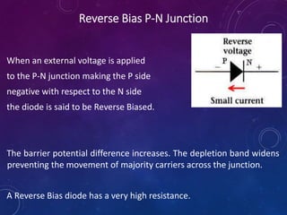
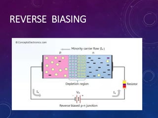


The document discusses various semiconductor concepts including n-type semiconductors, reverse biasing in diodes, and the operation of full wave bridge rectifiers. It emphasizes the advantages and disadvantages of full wave bridge rectifiers and describes the functioning and characteristics of Zener diodes. The document provides a comprehensive overview of diode operation, including their usage in different applications.


![[FULL ANIMATED(Download to view)] Unbiased diode, Forward biased , reverse bi...](https://cdn.slidesharecdn.com/ss_thumbnails/edc-141002103245-phpapp02-thumbnail.jpg?width=640&height=640&fit=bounds)