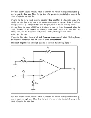
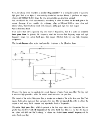
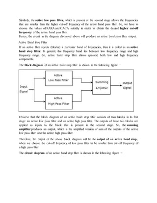
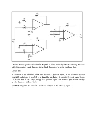
This document provides information about semiconductor materials and semiconductor devices. It discusses:
1. Semiconductors like silicon have electrical properties between conductors and insulators, with few free electrons. Doping semiconductors by adding impurity atoms can produce more free electrons or holes.
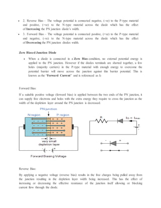
2. A PN junction diode is formed by joining a p-type and n-type semiconductor. It allows current to pass easily in one direction but blocks it in the other direction.
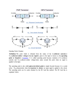
3. A transistor is a three-terminal semiconductor device that can amplify or switch electronic signals. Bipolar junction transistors (BJTs) have three terminals - base, collector, and emitter - and come in NPN
![From the above equation we can understand that when Vno-load occurs the load resistance is
infinite, that is, the out terminals are open circuited. Vfull-load occurs when the load resistance is
of the minimum value where voltage regulation is lost.
% Load Regulation = [(Vno-load - Vfull-load)/Vfull-load] * 100
2. Minimum Load Resistance – The load resistance at which a power supply delivers its full-
load rated current at rated voltage is referred to as minimum load resistance.
Minimum Load Resistance = Vfull-load/Ifull-load
The value of Ifull-load, full load current should never increase than that mentioned in the
datasheet of the power supply.
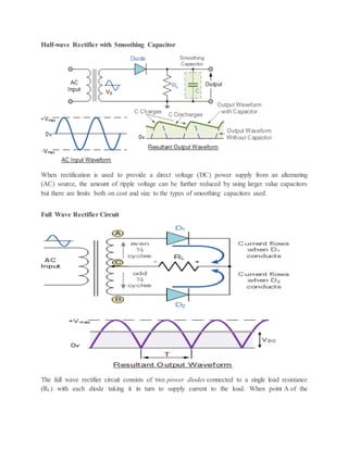
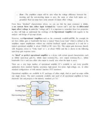
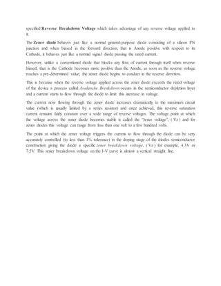
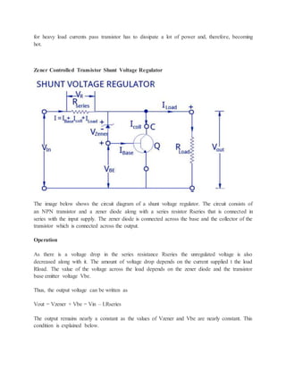
The Zener Diode:
A Semiconductor Diode blocks current in the reverse direction, but will suffer from premature
breakdown or damage if the reverse voltage applied across becomes too high
the Zener Diode or “Breakdown Diode”, as they are sometimes referred too, are basically the
same as the standard PN junction diode but they are specially designed to have a low and](https://image.slidesharecdn.com/appliedelectronicsstudymaterials-191117164535/85/Basic-of-Electronics-study-materials-59-320.jpg)
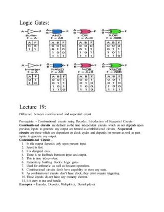
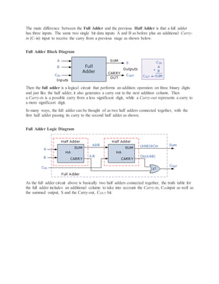
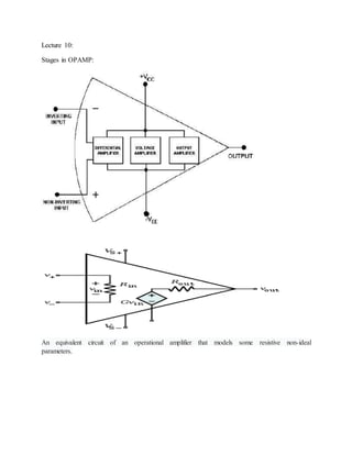
![Full Adder Truth Table with Carry
Then the Boolean expression for a full adder is as follows.
For the SUM (S) bit:
SUM = (A XOR B) XOR Cin = (A ⊕ B) ⊕ Cin
For the CARRY-OUT (Cout) bit:
CARRY-OUT = A AND B OR Cin(A XOR B
Flip Flops:
Flip flops are actually an application of logic gates. With the help of Boolean logic you can
create memory with them. Flip flops can also be considered as the most basic idea of a Random
Access Memory [RAM]. When a certain input value is given to them, they will be remembered
and executed, if the logic gates are designed correctly. A higher application of flip flops is
helpful in designing better electronic circuits.
The most commonly used application of flip flops is in the implementation of a feedback circuit.
As a memory relies on the feedback concept, flip flops can be used to design it.
There are mainly four types of flip flops that are used in electronic circuits. They are
1. The basic Flip Flop or S-R Flip Flop
2. Delay Flip Flop [D Flip Flop]
3. J-K Flip Flop
4. T Flip Flop
1. S-R Flip Flop
The SET-RESET flip flop is designed with the help of two NOR gates and also two NAND
gates. These flip flops are also called S-R Latch.](https://image.slidesharecdn.com/appliedelectronicsstudymaterials-191117164535/85/Basic-of-Electronics-study-materials-93-320.jpg)
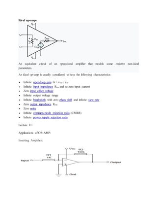
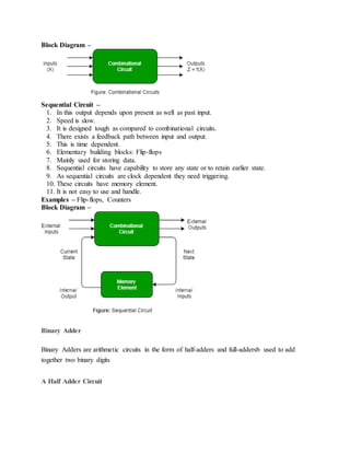
![ S-R Flip Flop using NOR Gate
The design of such a flip flop includes two inputs, called the SET [S] and RESET [R]. There are
also two outputs, Q and Q’. The diagram and truth table is shown below.
S-R Flip Flop using NOR Gate
From the diagram it is evident that the flip flop has mainly four states. They are
S=1, R=0—Q=1, Q’=0
This state is also called the SET state.
S=0, R=1—Q=0, Q’=1
This state is known as the RESET state.
In both the states you can see that the outputs are just compliments of each other and that the
value of Q follows the value of S.
S=0, R=0—Q & Q’ = Remember
If both the values of S and R are switched to 0, then the circuit remembers the value of S and R
in their previous state.](https://image.slidesharecdn.com/appliedelectronicsstudymaterials-191117164535/85/Basic-of-Electronics-study-materials-94-320.jpg)
![S=1, R=1—Q=0, Q’=0 [Invalid]
This is an invalid state because the values of both Q and Q’ are 0. They are supposed to be
compliments of each other. Normally, this state must be avoided.
S-R Flip Flop using NAND Gate
The circuit of the S-R flip flop using NAND Gate and its truth table is shown below.
S-R Flip Flop using NAND Gate
Like the NOR Gate S-R flip flop, this one also has four states. They are
S=1, R=0—Q=0, Q’=1
This state is also called the SET state.
S=0, R=1—Q=1, Q’=0
This state is known as the RESET state.
In both the states you can see that the outputs are just compliments of each other and that the
value of Q follows the compliment value of S.](https://image.slidesharecdn.com/appliedelectronicsstudymaterials-191117164535/85/Basic-of-Electronics-study-materials-95-320.jpg)
![S=0, R=0—Q=1, & Q’ =1 [Invalid]
If both the values of S and R are switched to 0 it is an invalid state because the values of both Q
and Q’ are 1. They are supposed to be compliments of each other. Normally, this state must
be avoided.
S=1, R=1—Q & Q’= Remember
If both the values of S and R are switched to 1, then the circuit remembers the value of S and R
in their previous state.
Clocked S-R Flip Flop
It is also called a Gated S-R flip flop.
The problems with S-R flip flops using NOR and NAND gate is the invalid state. This problem
can be overcome by using a bistable SR flip-flop that can change outputs when certain invalid
states are met, regardless of the condition of either the Set or the Reset inputs. For this, a clocked
S-R flip flop is designed by adding two AND gates to a basic NOR Gate flip flop. The circuit
diagram and truth table is shown below.](https://image.slidesharecdn.com/appliedelectronicsstudymaterials-191117164535/85/Basic-of-Electronics-study-materials-96-320.jpg)
![Clocked S-R Flip Flop
A clock pulse [CP] is given to the inputs of the AND Gate. When the value of the clock pulse is
‘0’, the outputs of both the AND Gates remain ‘0’. As soon as a pulse is given the value of CP
turns ‘1’. This makes the values at S and R to pass through the NOR Gate flip flop. But when the
values of both S and R values turn ‘1’, the HIGH value of CP causes both of them to turn to ‘0’
for a short moment. As soon as the pulse is removed, the flip flop state becomes intermediate.
Thus either of the two states may be caused, and it depends on whether the set or reset input of
the flip-flop remains a ‘1’ longer than the transition to ‘0’ at the end of the pulse. Thus the
invalid states can be eliminated.
2. D Flip Flop
The circuit diagram and truth table is given below.](https://image.slidesharecdn.com/appliedelectronicsstudymaterials-191117164535/85/Basic-of-Electronics-study-materials-97-320.jpg)
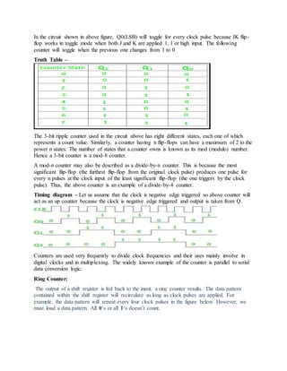
![J-K Flip Flop
A J-K flip flop can also be defined as a modification of the S-R flip flop. The only difference is
that the intermediate state is more refined and precise than that of a S-R flip flop.
The behavior of inputs J and K is same as the S and R inputs of the S-R flip flop. The letter J
stands for SET and the letter K stands for CLEAR.
When both the inputs J and K have a HIGH state, the flip-flop switch to the complement state.
So, for a value of Q = 1, it switches to Q=0 and for a value of Q = 0, it switches to Q=1.
The circuit includes two 3-input AND gates. The output Q of the flip flop is returned back as a
feedback to the input of the AND along with other inputs like K and clock pulse [CP]. So, if
the value of CP is ‘1’, the flip flop gets a CLEAR signal and with the condition that the value of](https://image.slidesharecdn.com/appliedelectronicsstudymaterials-191117164535/85/Basic-of-Electronics-study-materials-99-320.jpg)
![Q was earlier 1. Similarly output Q’ of the flip flop is given as a feedback to the input of the
AND along with other inputs like J and clock pulse [CP]. So the output becomes SET when the
value of CP is 1 only if the value of Q’ was earlier 1.
The output may be repeated in transitions once they have been complimented for J=K=1 because
of the feedback connection in the JK flip-flop. This can be avoided by setting a time duration
lesser than the propagation delay through the flip-flop. The restriction on the pulse width can be
eliminated with a master-slave or edge-triggered construction.
Lecture 20:
Counters:
A counter is basically used to count the number of clock pulses applied to a flip-flop. It can also
be used for Frequency divider, time measurement, frequency measurement, distance
measurement and also for generating square waveforms. In this, the flip-flops are asynchronous
counters and are supplied with different clock signals, there may be a delay in producing output.
Also, a few numbers of logic gates are needed to design asynchronous counters. So they are
elementary in design and also are less expensive.
Ripple counter –
A n-bit ripple counter can count up to 2n states. It is also known as MOD n counter. It is known
as ripple counter because of the way the clock pulse ripples its way through the flip-flops. Some
of the features of ripple counter are:
1. It is an asynchronous counter.
2. Different flip-flops are used with a different clock pulse.
3. All the flip-flops are used in toggle mode.
4. Only one flip-flop is applied with an external clock pulse and another flip-flop clock is
obtained from the output of the previous flip-flop.
5. The flip-flop applied with external clock pulse act as LSB (Least Significant Bit) in the
counting sequence.
A counter may be an up counter that counts upwards or can be a down counter that counts
downwards or can do both i.e.count up as well as count downwards depending on the input
control. The sequence of counting usually gets repeated after a limit. When counting up, for n-bit
counter the count sequence goes from 000, 001, 010, … 110, 111, 000, 001, … etc. When
counting down the count sequence goes in the opposite manner: 111, 110, … 010, 001, 000, 111,
110, … etc.
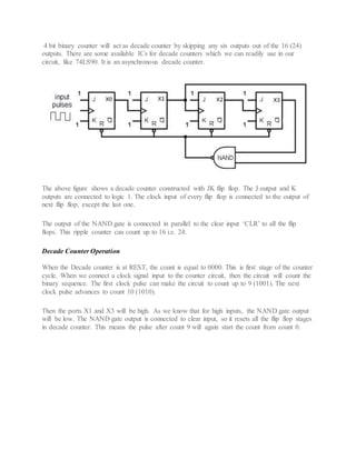
A 3-bit Ripple counter using JK flip-flop –](https://image.slidesharecdn.com/appliedelectronicsstudymaterials-191117164535/85/Basic-of-Electronics-study-materials-100-320.jpg)
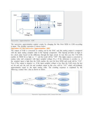
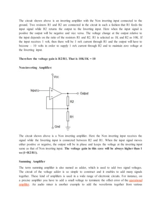
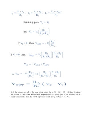
![The inverting input terminal of the op amp work as a summing amplifier for the ladder inputs. So
we can get out put voltage by bellow equation.
V0 = VR*(RF/R)[b1/21 + b2/22 + b3/23 + b4/24]
Successive Approximation ADC (Analog to Digital Converter)
Successive approximation ADC is the advanced version of Digital ramp type ADC which is
designed to reduce the conversion and to increase speed of operation. The major draw of digital
ramp ADC is the counter used to produce the digital output will be reset after every sampling
interval. The normal counter starts counting from 0 and increments by one LSB in each count,
this result in 2N clock pulses to reach its maximum value.
In successive approximation ADC the normal counter is replaced with successive approximation
register as shown in below figure.](https://image.slidesharecdn.com/appliedelectronicsstudymaterials-191117164535/85/Basic-of-Electronics-study-materials-114-320.jpg)