Diode Applications & Transistor Basics
•
6 likes•3,215 views

1. The document discusses the V-I characteristics of a p-n junction diode and describes its behavior under zero external voltage, forward bias, and reverse bias. 2. Rectifiers are introduced as circuits that convert AC to DC. Half-wave and full-wave rectifiers are described, including their circuit arrangements and operations. Centre-tap and bridge configurations are covered for full-wave rectification. 3. Zener diodes are discussed as properly doped diodes with a sharp breakdown voltage. They are always connected in reverse bias and have a defined zener voltage.

Recommended
More Related Content
What's hot
What's hot (20)
Similar to Diode Applications & Transistor Basics
Similar to Diode Applications & Transistor Basics (20)
More from A B Shinde
More from A B Shinde (20)
Recently uploaded
Recently uploaded (20)
Diode Applications & Transistor Basics
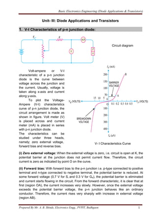
- 1. Basic Electronics Engineering (Diode Applications & Transistors) Prepared By Mr. A. B. Shinde, Electronics Engg., PVPIT, Budhgaon 1 Unit- III: Diode Applications and Transistors 1. V-I Characteristics of p-n junction diode: Circuit diagram Volt-ampere or V-I characteristic of a p-n junction diode is the curve between voltage across the junction and the current. Usually, voltage is taken along x-axis and current along y-axis. To plot the Voltage- Ampere (V-I) characteristics curve of p-n junction diode, the circuit arrangement is made as shown in figure. Volt meter (V) is placed across and current meter (mA) is placed in series with p-n junction diode. The characteristics can be studied under three heads, namely; zero external voltage, forward bias and reverse bias. V- I Characteristics Curve (i) Zero external voltage: When the external voltage is zero, i.e. circuit is open at K, the potential barrier at the junction does not permit current flow. Therefore, the circuit current is zero as indicated by point O on the curve. (ii) Forward bias: With forward bias to the p-n junction i.e. p-type connected to positive terminal and n-type connected to negative terminal, the potential barrier is reduced. At some forward voltage (0.7 V for Si and 0.3 V for Ge), the potential barrier is eliminated and current starts flowing in the circuit. From the forward characteristic, it is clear that at first (region OA), the current increases very slowly. However, once the external voltage exceeds the potential barrier voltage, the p-n junction behaves like an ordinary conductor. Therefore, the current rises very sharply with increase in external voltage (region AB).
- 2. Basic Electronics Engineering (Diode Applications & Transistors) Prepared By Mr. A. B. Shinde, Electronics Engg., PVPIT, Budhgaon 2 (iii) Reverse bias: With reverse bias to the p-n junction i.e. p-type connected to negative terminal and n-type connected to positive terminal, potential barrier at the junction is increased; hence junction resistance becomes very high hence, a very small current (few μA) flows in the circuit. If reverse voltage is increased continuously, the kinetic energy of electrons (minority carriers) may become high enough to knock out electrons from the semiconductor atoms. At this stage breakdown of the junction occurs, characterised by a sudden rise of reverse current. Important Terms (i) Breakdown voltage: It is the minimum reverse voltage at which p-n junction breaks down with sudden rise in reverse current. (ii) Knee voltage: It is the forward voltage at which the current through the junction starts to increase rapidly. It is clear from the above graph that knee voltage for silicon diode is 0.7 V and 0.3 V for germanium diode. If the forward voltage exceeds the knee voltage, the current starts increasing rapidly. 2. Rectifiers: Rectifier is circuit which converts a.c. signal into d.c. signal. The supply voltage is sinusoidal and has a frequency of 50 HZ. It is used for lighting, heating and electric motors. But there are many applications (e.g. electronic circuits) where d.c. supply is needed. The following two rectifier circuits can be used: i. Half-wave rectifier ii. Full-wave rectifier 2.1. Half-Wave Rectifier: Here, the rectifier conducts current only during the positive half-cycles of input a.c. supply. The negative half-cycles of a.c. supply are suppressed i.e. during negative half- cycles, no current is conducted and hence no voltage appears across the load. Therefore, current always flows in one direction (i.e. d.c.) through the load though after every half-cycle.
- 3. Basic Electronics Engineering (Diode Applications & Transistors) Prepared By Mr. A. B. Shinde, Electronics Engg., PVPIT, Budhgaon 3 Input ac signal Rectified output Half wave rectifier circuit diagram Circuit Arrangement: The circuit diagram of half wave rectifier is as shown in figure. The a.c. supply is applied in series with the diode and load resistance RL. Input, a.c. supply is given through a transformer. The use of transformer permits two advantages. Firstly, it allows us to step up or step down the a.c. input voltage as the situation demands. Secondly, the transformer isolates the rectifier circuit from power line and thus reduces the risk of electric shock. Operation: The a.c. voltage across the secondary winding AB changes polarities after every half-cycle. During the positive half cycle of input a.c. voltage, end A becomes positive w.r.t. end B. This makes the diode forward biased and hence it conducts current. During the negative half cycle, end A is negative w.r.t. end B. Under this condition, the diode is reverse biased and it conducts no current. Therefore, current flows through the diode during positive half-cycles of input a.c. voltage only. In this way, current flows through load RL always in the same direction. Hence d.c. output is obtained across RL. It may be noted that output across the load is pulsating d.c. Advantages: 1. Simple circuit arrangement. 2. Low cost Disadvantages: 1. The pulsating current in the load contains alternating component whose basic frequency is equal to the supply frequency. 2. The a.c. supply delivers power only half the time.
- 4. Basic Electronics Engineering (Diode Applications & Transistors) Prepared By Mr. A. B. Shinde, Electronics Engg., PVPIT, Budhgaon 4 2.2. Full-Wave Rectifier: In full-wave rectification, current flows through the load in the same direction for both half-cycles of input a.c. voltage. For the positive half cycle of input voltage, one diode supplies current to the load and for the negative half-cycle, the other diode does so; current being always in the same direction through the load. Therefore, a full-wave rectifier utilises both half-cycles of input a.c. voltage to produce the d.c. output. The following two circuits are commonly used for full-wave rectification: i. Centre-tap full-wave rectifier ii. Full-wave bridge rectifier 2.2.1. Centre-Tap Full-Wave Rectifier: Circuit arrangement: The circuit has two diodes D1 and D2 as shown in figure. A centre tapped secondary winding AB is used with two diodes connected so that each uses one half-cycle of input a.c. voltage. The load resistance RL is connected between the common point of cathode of both diodes and centre tap of transformer. Operation: During positive half cycle During negative half cycle During the positive half-cycle, the point A becomes positive and point B becomes negative. This makes the diode D1 forward biased and diode D2 reverse biased. Therefore, diode D1 conducts while diode D2 does not. The conventional current flow is through diode D1, load resistor RL and the upper half of secondary winding as shown by the dotted arrows. During the negative half-cycle, point A becomes negative and point B becomes positive. Therefore, diode D2 conducts while diode D1 does not. The conventional current flow is through diode D2, load RL and lower half winding as shown by solid arrows. From the figure, it is clear that current in the load RL flows in the same direction for both half-cycles of input a.c. voltage. Therefore, d.c. is obtained across the load RL.
- 5. Basic Electronics Engineering (Diode Applications & Transistors) Prepared By Mr. A. B. Shinde, Electronics Engg., PVPIT, Budhgaon 5 Advantages: 1. Full wave rectification i.e. high efficiency Disadvantages 1. It is difficult to locate the centre tap on the secondary winding. 2. The d.c. output is small as each diode utilises only one-half of the transformer secondary voltage. 3. The diodes used must have high peak inverse voltage. 2.2.2. Full-Wave Bridge Rectifier: Circuit arrangement: The need for a centre tapped transformer is eliminated in the bridge rectifier. It contains four diodes D1, D2, D3 and D4 connected to form bridge as shown in figure. The a.c. input is applied to the diagonally opposite ends of the bridge through the transformer. Between other two ends of the bridge, the load resistance RL is connected. Operation: During the positive half-cycle, point P of the secondary winding becomes positive and point Q becomes negative. This makes diodes D1 and D3 forward biased while diodes D2 and D4 are reverse biased. Therefore, only diodes D1 and D3 conduct. The conventional current flow is shown by dotted arrows. During the negative half-cycle, point P becomes negative and point Q becomes positive. This makes diodes D2 and D4 forward biased whereas diodes D1 and D3 are reverse biased. Therefore, only diodes D2 and D4 conduct. The current flow is shown by the solid arrows. It may be seen that again current flows from A to B through the load i.e. in the same direction as for the positive half- cycle. Therefore, d.c. output is obtained across load RL. During positive half cycle During negative half cycle
- 6. Basic Electronics Engineering (Diode Applications & Transistors) Prepared By Mr. A. B. Shinde, Electronics Engg., PVPIT, Budhgaon 6 Advantages i. The need for centre-tapped transformer is eliminated. ii. The output is twice that of the centre-tap circuit for the same secondary voltage. iii. The PIV is one-half that of the centre-tap circuit (for same d.c. output). Disadvantages i. It requires four diodes. ii. As during each half-cycle of a.c., two diodes are conducting therefore, voltage drop will be twice as compared to centre tap circuit. 2.2.3. Comparison of Rectifiers: 3. Zener Diode Regulator: A properly doped crystal diode which has a sharp breakdown voltage is known as a zener diode. The following points may be noted about the zener diode: i. A zener diode is like an ordinary diode except that it is properly doped so as to have a sharp breakdown voltage. ii. A zener diode is always connected in reverse i.e. it is always reverse biased. iii. A zener diode has sharp breakdown voltage, called zener voltage VZ. iv. When forward biased, its characteristics are just like ordinary diode.
- 7. Basic Electronics Engineering (Diode Applications & Transistors) Prepared By Mr. A. B. Shinde, Electronics Engg., PVPIT, Budhgaon 7 3.1. Zener Diode regulator: A zener diode can be used as a voltage regulator to provide a constant voltage from a source whose voltage may vary. The circuit arrangement is as shown in figure. The zener diode with voltage VZ is connected in reverse across the load RL. The series resistance R absorbs the output voltage fluctuations so as to maintain constant voltage across the load. It may be noted that the zener will maintain a constant voltage VZ (= E0) across the load, provided that the input voltage should not fall below VZ. Circuit arrangement for Zener regulator Equivalent Circuit 4. Voltage Multiplier: Diodes and Capacitors can be used to build a circuit that will provide a d.c output which is multiple of the peak input a.c. voltage. Such a circuit is called a voltage multiplier. When a voltage multiplier increases the peak input voltage by a factor n, the peak input current is decreased by approximately the same factor. Thus the actual power output from a voltage multiplier will never be greater than the input power. In fact, there are losses in the circuit (e.g. in diodes, capacitors etc.) so that the output power will actually be less than the input power. 4.1. Half-Wave Voltage Doubler: A half-wave voltage doubler consists of two diodes and two capacitors connected as shown in figure. The basic idea in a voltage multiplier is to charge each capacitor to the peak input a.c. voltage and to arrange the capacitors so that their stored voltages will add. Operation: 1. During the negative half-cycle of a.c. input voltage, diode D1 is forward biased and diode D2 is reverse biased. Therefore, diode D1 can be represented by a short and diode D2 as an open. 2. C1 will charge until voltage across it becomes equal to peak value of source voltage Vs (p).
- 8. Basic Electronics Engineering (Diode Applications & Transistors) Prepared By Mr. A. B. Shinde, Electronics Engg., PVPIT, Budhgaon 8 3. During positive half-cycle, D1 is reverse biased and D2 is forward. Now C1 (charged to source voltage (Vs (p)) act as series-aiding voltage sources. Thus C2 will be charged to the sum of the series peak voltages i.e. 2 VS (p). 4. When VS returns to its original polarity (i.e. negative half-cycle), D2 is again turned off (i.e. reverse biased). With D2 turned off, the only discharge path for C2 is through the load resistance RL. The time required to discharge C2 (RL.C2) is too large, hence C2 always appears like it is fully charged. 4.2. Full-Wave Voltage Doubler: The circuit arrangement for full wave voltage doubler is as shown in the figure. Here, two diodes and two capacitors are used. Each capacitor is charged during each half cycle of input Operation: When the sinusoidal input voltage is positive, capacitor C1 charges up through diode D1 and when the sinusoidal voltage is negative, capacitor C2 charges up through diode, D2. The output voltage is taken across the series combination of two capacitors. As C1 is charged to the Vi and C2 is also charged to Vi, total output becomes 2Vi. 5. Clipping Circuits: The circuit with which the waveform is shaped by removing (or clipping) a portion of the applied wave is known as a clipping circuit. The clippers are used to remove signal voltages above or below a specified level. The important diode clippers are i. Positive clipper ii. Biased clipper iii. Combination clipper. 5.1. Positive clipper: A positive clipper is the circuit which removes the positive half-cycles of the input signal. Figure shows the typical circuit of a positive clipper. During the positive half-cycle of the input voltage, the diode is forward biased and conducts heavily. Therefore, the voltage across the diode and hence across the load RL is zero. Hence output voltage during positive half-cycles is zero. During the negative half-cycle of the input voltage, the diode is reverse biased and behaves as an open circuit, hence input will appear as it is at the output.
- 9. Basic Electronics Engineering (Diode Applications & Transistors) Prepared By Mr. A. B. Shinde, Electronics Engg., PVPIT, Budhgaon 9 Output is calculated with equation: Generally, RL is much greater than R. Output voltage = − Vm 5.2. Negative clipper: A negative clipper is that which removes the negative half-cycles of the input voltage. Figure shows the typical circuit of a negative clipper using a diode. During the positive half-cycle of the input voltage, the diode is reverse biased and acts as open circuit. Therefore, the voltage across load RL is same as that of input. During the negative half-cycle of the input voltage, the diode is forward biased and behaves as short circuit; hence the output across RL is zero. Output is calculated with equation: Generally, RL is much greater than R., hence Output voltage = Vm
- 10. Basic Electronics Engineering (Diode Applications & Transistors) Prepared By Mr. A. B. Shinde, Electronics Engg., PVPIT, Budhgaon 10 5.3. Biased positive clipper: Sometimes it is desired to remove a small portion of positive or negative half-cycle instead of removing complete half-cycle. For this purpose, biased clipper is used. Figure shows the circuit of a biased clipper using battery of V volts. A portion of each positive half-cycle will be clipped. The diode will conduct heavily so long as input voltage is greater than +V. When input voltage is greater than +V, the diode behaves as a short and the output equals +V. The output will stay at +V so long as the input voltage is greater than +V. During the period the input voltage is less than +V, the diode is reverse biased and behaves as an open. Therefore, most of the input voltage appears across the output. In this way, the biased positive clipper removes input voltage above +V. During the negative half-cycle of the input voltage, the diode remains reverse biased. Therefore, almost entire negative half-cycle appears across the load. 5.4. Biased negative clipper: 5.5. Combination clipper: It is a combination of biased positive and negative clippers. With a combination clipper, a portion of both positive and negative half-cycles of input voltage can be removed or clipped as shown in figure.
- 11. Basic Electronics Engineering (Diode Applications & Transistors) Prepared By Mr. A. B. Shinde, Electronics Engg., PVPIT, Budhgaon 11 When positive input voltage is greater than + V1, diode D1 conducts heavily while diode D2 remains reverse biased. Therefore, a voltage +V1 appear across the load. This output stays at +V1, as long as the input voltage exceeds +V1. On the other hand, during the negative half- cycle, the diode D2 will conduct heavily and the output stays at − V2 as long as the input voltage is greater than − V2. Between + V1 and − V2 neither diode is on. Therefore, in this condition, most of the input voltage appears across the load. 5.6. Applications of Clippers: In general, clippers are used to perform one of the following two functions: Changing the shape of a waveform: Clippers can alter the shape of a waveform. For example, a clipper can be used to convert a sine wave into a rectangular wave, square wave etc. Circuit transient protection: Transients can cause considerable damage to many types of circuits e.g., a digital circuit. In that case, a clipper diode can be used to prevent the transient form reaching that circuit. 6. Clamping Circuits: A circuit that places either the positive or negative peak of a signal at a desired d.c. level is known as a clamping circuit. 6.1. Positive Clamper: Figure shows the circuit of a positive clamper. The input signal is assumed to be a square wave with time period T. The clamped output is obtained across RL. The values of C and RL are so selected that time constant T = C.RL is very large. This means that voltage across the capacitor will not discharge significantly during the interval the diode is non-conducting.
- 12. Basic Electronics Engineering (Diode Applications & Transistors) Prepared By Mr. A. B. Shinde, Electronics Engg., PVPIT, Budhgaon 12 Operation: During the negative half-cycle of the input signal, the diode is forward biased i.e. acts as a short circuit. The charging time constant (= C.Rf , where Rf = forward resistance of the diode) is very small so that the capacitor will charge to V volts very quickly, therefore, Vout = 0 V. When the input switches to +V state (i.e. positive half-cycle), the diode is reverse biased and behaves as an open circuit. Since the discharging time constant (= C.RL) is much greater than the time period of the input signal, the capacitor remains almost fully charged to V volts during the off time of the diode. By applying Kirchhoff’s voltage law to the input loop, we have, V + V - Vout = 0 Vout = 2V The resulting waveform is as shown in figure. It is clear that, it is a positively clamped output. That is to say the input signal has been pushed upward by V volts so that negative peaks fall on the zero level. 6.2. Negative Clamper Figure shows the circuit of a negative clamper. The clamped output is taken across RL. During the positive half-cycle of the input signal, the diode is forward biased i.e. acts as a short circuit. The charging time constant (= C.Rf) is very small so that the capacitor will charge to V volts very quickly, therefore, Vout = 0. When the input switches to − V state (i.e., negative half-cycle), the diode is reverse biased and behaves as an open circuit. Since the discharging time constant (= C.RL) is much greater than the time period of the input signal, the capacitor almost remains fully charged to V volts during the off time of the diode.
- 13. Basic Electronics Engineering (Diode Applications & Transistors) Prepared By Mr. A. B. Shinde, Electronics Engg., PVPIT, Budhgaon 13 By applying Kirchhoff ’s voltage law to the input loop, we get, - V - V - Vout = 0 Vout = - 2 V The resulting waveform is as shown in figure. Note that total swing of the output signal is equal to the total swing of the input signal. 7. Transistors: When a third doped element is added to a crystal diode in such a way that two p- n junctions are formed, the resulting device is known as a transistor. 7.1. Introduction Transistors are far smaller than vacuum tubes, have no filament and hence need no heating power and may be operated in any position. A transistor consists of two p-n junctions formed by sandwiching either p-type or n-type semiconductor between a pair of opposite types. Accordingly; there are two types of transistors, namely; (i) n-p-n transistor (ii) p-n-p transistor An n-p-n transistor is composed of two n-type semiconductors separated by a thin section of p-type as shown in left side figure. However, a p-n-p transistor is formed by two p- sections separated by a thin section of n-type as shown in right side figure. Symbols: npn transistor pnp transistor 7.2. Transistor Terminals: A transistor (pnp or npn) has three sections of doped semiconductors. The section on one side is the emitter and the section on the opposite side is the collector. The middle section is called the base and forms two junctions with the emitter and collector. Emitter: The section that supplies charge carriers (electrons or holes) is called the emitter. The emitter is always forward biased w.r.t. base so that it can supply a large number of majority carriers.
- 14. Basic Electronics Engineering (Diode Applications & Transistors) Prepared By Mr. A. B. Shinde, Electronics Engg., PVPIT, Budhgaon 14 Collector: The section that collects the charges carriers is called the collector. The collector is always reverse biased. Its function is to remove charges from its junction with the base. Base: The middle section which forms two p-n junctions between the emitter and collector is called the base. The base-emitter junction is forward biased, allowing low resistance for the emitter circuit. The base-collector junction is reverse biased and provides high resistance in the collector circuit. 7.3. Origin of the name “Transistor” (Why transistor s called as “transistor”?) A transistor has two p-n junctions. One junction is forward biased and the other is reverse biased. The forward biased junction has a low resistance path whereas a reverse biased junction has a high resistance path. The weak signal is introduced in the low resistance circuit and output is taken from the high resistance circuit. Therefore, a transistor transfers a signal from a low resistance to high resistance. The prefix ‘trans’ means the signal transfer property of the device while ‘istor’ classifies it as a solid element. Transfer + resistor = Transistor. 7.4. Working of npn transistor: Figure shows the npn transistor with forward bias to emitter-base junction and reverse bias to collector- base junction. The forward bias causes the electrons in the n-type emitter to flow towards the base. This constitutes the emitter current IE. As these electrons flow through the p-type base, they tend to combine with holes. As the base is lightly doped and very thin, therefore, only a few electrons (less than 5%) combine with holes to constitute base current IB. The remaining electrons (more than 95%) crosses the junction and reaches the collector region to constitute collector current IC. In this way, almost the entire emitter current flows in the collector circuit. It is clear that emitter current is the sum of collector and base currents i.e. IE = IB + IC 7.5. Working of pnp transistor: Figure shows the basic connection of a pnp transistor. The forward bias causes the holes in the p- type emitter to flow towards the base.
- 15. Basic Electronics Engineering (Diode Applications & Transistors) Prepared By Mr. A. B. Shinde, Electronics Engg., PVPIT, Budhgaon 15 This constitutes the emitter current IE. As these holes cross into n-type base, they tend to combine with the electrons. As the base is lightly doped and very thin, therefore, only a few holes (less than 5%) combine with the electrons. The remaining holes (more than 95%) crosses the junction and reaches collector region to constitute collector current IC. In this way, almost the entire emitter current flows in the collector circuit. Current conduction within pnp transistor is by holes. However, in the external connecting wires, the current is still by electrons. 8. Transistor Configurations: There are three leads in a transistor viz., emitter, base and collector. However, when a transistor is to be connected in a circuit, we require four terminals; two for the input and two for the output. This difficulty is overcome by making one terminal of the transistor common to both input and output terminals. Accordingly; a transistor can be connected in a circuit in the following three ways: i. Common Base Configuration ii. Common Emitter Configuration iii. Common Collector Configuration 8.1. Common Base Connection (CB): In this circuit arrangement, input is applied between emitter and base and output is taken from collector and base. Here, base of the transistor is common to both input and output circuits and hence the name common base (CB) connection. Figure shows common base npn transistor configuration. Current amplification factor (α): It is the ratio of output current to input current. In a common base connection, the input current is the emitter current IE and output current is the collector current IC. The ratio of change in collector current (∆IC) to the change in emitter current (∆IE) at constant collector base voltage VCB is known as current amplification factor i.e. 8.2. Common Emitter Connection (CE): In this circuit arrangement, input is applied between base and emitter and output is taken from the collector and emitter. Here, emitter of the transistor is common to both input and output circuits and hence the name common emitter (CE) connection. Figure shows common emitter npn transistor circuit.
- 16. Basic Electronics Engineering (Diode Applications & Transistors) Prepared By Mr. A. B. Shinde, Electronics Engg., PVPIT, Budhgaon 16 Base current amplification factor (β): In common emitter connection, input current is IB and output current is IC. The ratio of change in collector current (∆IC) to the change in base current (∆IB) is known as base current amplification factor i.e. In almost any transistor, less than 5% of emitter current flows as the base current. Therefore, the value of β is generally greater than 20. Usually, its value ranges from 20 to 500. Base current = IB Collector current = β.IB + ICEO Emitter current = Collector current + Base current = (β.IB + ICEO) + IB = (β+ 1) IB + ICEO Relation between β and α: A simple relation exists between β and α. This can be derived as follows: It is clear that as α approaches unity, β approaches infinity. In other words, the current gain in common emitter (CE) connection is very high. Hence, this circuit arrangement (CE) is used in about 90 to 95 percent of all transistor applications. Example 1: Find the value of β if (i) α = 0.9 (ii) α = 0.98 (iii) α = 0.99. Example 2: Calculate IE in a transistor for which β = 50 and IB = 20 μA.
- 17. Basic Electronics Engineering (Diode Applications & Transistors) Prepared By Mr. A. B. Shinde, Electronics Engg., PVPIT, Budhgaon 17 8.3. Common Collector Connection: In this circuit arrangement, input is applied between base and collector while output is taken between the emitter and collector. Here, collector of the transistor is common to both input and output circuits and hence the name common collector (CC) connection. Figure shows common collector npn transistor. Current amplification factor (γ). The ratio of change in emitter current (∆IE) to the change in base current (∆IB) is known as current amplification factor in common collector (CC) arrangement i.e. 8.4. Comparison of Transistor Connections: 9. Transistor as an amplifier: Figure shows the common emitter (CE) npn amplifier circuit. Battery VBB is connected in the input circuit in addition to the signal voltage. This d.c. voltage is known as bias voltage and its magnitude is such that it always keeps the emitter-base junction forward biased regardless of the polarity of the signal source.
- 18. Basic Electronics Engineering (Diode Applications & Transistors) Prepared By Mr. A. B. Shinde, Electronics Engg., PVPIT, Budhgaon 18 Operation: During the positive half-cycle of the input signal, the forward bias across the emitter-base junction is increased. Therefore, more electrons flow from the emitter to the collector via the base. This causes an increase in collector current. The increased collector current produces a greater voltage drop across the collector load resistance RC. However, during the negative half-cycle of the input signal, the forward bias across emitter-base junction is decreased. Therefore, collector current also decreases. This results in the decreased output voltage. Hence, an amplified output is obtained across the load. 9.1. Transistor Testing: An ohmmeter can be used to check (test) the transistor. We know that base- emitter junction of a transistor is forward biased while collector-base junction is reverse biased. Therefore, forward biased base-emitter junction should have low resistance and reverse biased collector-base junction should register a much higher resistance. Figure shows the process of testing an npn transistor with an ohmmeter. i. The forward biased base-emitter junction should show low resistance approx. 100 Ω to 1 kΩ. ii. The reverse biased collector-base junction should higher resistance approx. 100 kΩ or higher. 10. Transistor Load Line Analysis: In the transistor circuit analysis, it is generally required to determine the collector current for various collector-emitter voltages. A load line method is most commonly used. This method is quite easy and is frequently used in the analysis of transistor applications. Consider a common emitter npn transistor circuit shown in figure, where no signal is applied. The output characteristics of this circuit are shown in graph. The value of collector-emitter voltage VCE at any time is given by; VCE = VCC – IC RC As VCC and RC are fixed values, therefore, it is a first degree equation and can be represented by a straight line on the output characteristics. This is known as d.c. load line. To add load line, we need two end points of the straight line. These two points can be located as under :
- 19. Basic Electronics Engineering (Diode Applications & Transistors) Prepared By Mr. A. B. Shinde, Electronics Engg., PVPIT, Budhgaon 19 i. When the collector current IC = 0, then collector-emitter voltage is maximum and is equal to VCC i.e. Max. VCE = VCC – IC.RC = VCC (as IC = 0) This gives the first point B (OB = VCC) on the collector-emitter voltage axis as shown in graph. ii. When collector-emitter voltage VCE = 0, the collector current is maximum and is equal to VCC /RC i.e. VCE = VCC - IC.RC or 0 = VCC - IC RC Max. IC = VCC / RC Cut off: The point where the load line intersects the IB = 0 curve is known as cut off. At this point, IB = 0 and only small collector current (i.e. collector leakage current ICEO) exists. At cut off, the base-emitter junction no longer remains forward biased and normal transistor action is lost. The collector-emitter voltage is nearly equal to VCC i.e. VCE (cut off) = VCC Saturation: The point where the load line intersects the IB = IB(sat) curve is called saturation. At this point, the base current is maximum and so is the collector current. At saturation, collector base junction no longer remains reverse biased and normal transistor action is lost. Active region: The region between cut off and saturation is known as active region. In the active region, collector-base junction remains reverse biased while base-emitter junction remains forward biased. Consequently, the transistor will function normally in this region. Operating Point: The zero signal values of IC and VCE are known as the operating point. It is called operating point because the variations of and VCE take place about this point when signal is applied. It is also called quiescent point or Q-point because it is the point on IC − VCE characteristic when the transistor is silent i.e. in the absence of the signal.
- 20. Basic Electronics Engineering (Diode Applications & Transistors) Prepared By Mr. A. B. Shinde, Electronics Engg., PVPIT, Budhgaon 20 The point Q describes the actual state of affairs in the circuit in the zero signal conditions and is called the operating point. For IB = 5 μA, the zero signal values are: VCE = OC volts IC = OD mA It follows, therefore, that the zero signal values of IC and VCE (i.e. operating point) are determined by the point where d.c. load line intersects the proper base current curve. 11. Transistor Biasing : 11.1. Faithful Amplification: The process of raising the strength of a weak signal without any change in its general shape is known as faithful amplification. The transistor will function properly if its input circuit (i.e. base-emitter junction) remains forward biased and output circuit (i.e. collector-base junction) remains reverse biased at all times. This is then the key factor for achieving faithful amplification. To ensure faithful amplification, the following basic conditions must be satisfied: a. Proper zero signal collector current b. Minimum proper base-emitter voltage (VBE) at any instant c. Minimum proper collector-emitter voltage (VCE) at any instant 11.2. Transistor Biasing: Introduction The fulfilment of conditions for achieving faithful amplification is called as transistor biasing. The basic purpose of transistor biasing is to keep the base-emitter junction properly forward biased and collector-base junction properly reverse biased during the application of signal. The circuit which provides proper biasing to the transistor is known as biasing circuit. It may be noted that transistor biasing is very essential for the proper operation of transistor in any circuit. 11.3. Methods of Transistor Biasing: Normally, transistor circuit should have a single source of supply (VCC). The following are the most commonly used methods of obtaining transistor biasing from one source of supply (i.e. VCC): i. Base resistor method ii. Biasing with collector-feedback resistor iii. Voltage-divider bias In all these methods, the same basic principle is employed i.e. required value of base current (and hence IC) is obtained from VCC in the zero signal conditions. The value of collector load RC is selected keeping in view that VCE should not fall below 0.5 V for germanium transistors and 1 V for silicon transistors.
- 21. Basic Electronics Engineering (Diode Applications & Transistors) Prepared By Mr. A. B. Shinde, Electronics Engg., PVPIT, Budhgaon 21 11.3.1. Base Resistor Method: In this method, a high resistance RB (several hundred kΩ) is connected between the base and +ve end of supply for npn transistor (See figure) and between base and negative end of supply for pnp transistor. Here, the required zero signal base current is provided by VCC and it flows through RB. It is because now base is positive w.r.t. emitter i.e. base-emitter junction is forward biased. The required value of zero signal base current IB (and hence IC = β.IB) can be made to flow by selecting the proper value of base resistor RB. Advantages: 1. This biasing circuit is very simple as only one resistance RB is required. 2. Biasing conditions can easily be set and the calculations are simple. 3. There is no loading of the source by the biasing circuit since no resistor is employed across base-emitter junction. Disadvantages: 1. This method provides poor stabilisation. It is because there is no means to stop a self increase in collector current due to temperature rise and individual variations. 2. The stability factor is very high. Therefore, there are strong chances of thermal runaway. 11.3.2. Biasing with Collector Feedback Resistor: In this method, one end of RB is connected to the base and the other end to the collector as shown in figure. Here, the required zero signal base current is determined not by VCC but by the collector-base voltage VCB. It is clear that VCB forward biases the base-emitter junction and hence base current IB flows through RB. This causes the zero signal collector current to flow in the circuit. Advantages: 1. It is a simple method as it requires only one resistance RB. 2. This circuit provides some stabilisation of the operating point as discussed below : VCE = VBE + VCB Disadvantages: 1. The circuit does not provide good stabilisation because stability factor is fairly high, therefore, the operating point does change. 2. This circuit provides a negative feedback which reduces the gain of the amplifier. During the positive half-cycle of the signal, the collector current increases. The
- 22. Basic Electronics Engineering (Diode Applications & Transistors) Prepared By Mr. A. B. Shinde, Electronics Engg., PVPIT, Budhgaon 22 increased collector current would result in greater voltage drop across RC. This will reduce the base current and hence collector current. 11.3.3. Voltage Divider Bias Method: This is the most widely used method of providing biasing and stabilisation to a transistor. In this method, two resistances R1 and R2 are connected across the supply voltage VCC (refer the figure) and provide biasing. The emitter resistance RE provides stabilisation. The name ‘‘voltage divider’’ comes from the voltage divider formed by R1 and R2. The voltage drop across R2 forward biases the base-emitter junction. This causes the base current and hence collector current flows in the zero signal conditions. 12. Bias Compensation Methods : The stabilization of biasing techniques occurs due to negative feedback action. The negative feedback, although improves the stability of operating point, it reduces the gain of the amplifier. The gain of the amplifier is a very important consideration while designing but in some cases the gain should not be reduced. In such cases, we need to use compensation techniques to stabilize the Q-point instead of using d.c. biasing circuits. In compensation techniques, temperature sensitive devices like diodes and thermistors are used. Sometimes a combination of biasing circuit and temperature sensitive devices are used. 12.1. Bias Compensation using diode: The figure shows the circuit diagram of a transistor amplifier with diode D used for compensation of variation in ICO. Here, diode is reverse biased by base emitter junction voltage (VBE). It allows reverse saturation current to flow. When temperature increases, the reverse saturation current (ICO) through the transistor also increases. This in turn also increases the leakage current through the diode, which will reduce base current (IB). Therefore the collector current is dependant only on the temperature.
- 23. Basic Electronics Engineering (Diode Applications & Transistors) Prepared By Mr. A. B. Shinde, Electronics Engg., PVPIT, Budhgaon 23 Now the base current is, IB = I − IO I = VCC−VBE / R = VCC / R = Constant Substituting the above value in the expression for collector current, IC=β (I − IO) + (1 + β) ICO If β = 1, IC = βI − βIO + βICO I is almost constant and if IO of diode and ICO of transistor track each other over the operating temperature range, then IC remains constant. 12.2. Thermistor Compensation Figure shows the thermistor compensation technique. The thermistor has negative temperature coefficient i.e. its resistance decreases with increase in temperature. Thermistor is placed in parallel with R2 or in place of R2. The values of R1 and R2 are selected in such a way that it will provide correct bias at normal temperature. As temperature increases, the voltage drop across RT decreases. This in turn reduces the forward bias across base-emitter junction, which will further reduce the base current and hence collector current. IC= β.IB + (β+ 1) ICEO The equation shows if there is increase in ICO and decrease in IB keeps IC almost constant. 13. Transistor as switch : Very often, bipolar junction transistors are used as electronic switches. With the help of such a switch, a given load can be turned ON or OFF by a small control signal. This control signal might be the one appearing at the output of a digital logic or a microprocessor.
- 24. Basic Electronics Engineering (Diode Applications & Transistors) Prepared By Mr. A. B. Shinde, Electronics Engg., PVPIT, Budhgaon 24 The power level of the control signal is usually very small and, hence, it is incapable of switching the load directly. However, such a control signal is certainly capable of providing enough base drive to switch a transistor ON or OFF and, hence, the transistor is made to switch the load. When using BJT as a switch, usually two levels of control signal are employed. With one level, the transistor operates in the cut- off region (open) whereas with the other level, it operates in the saturation region and acts as a short circuit. Figure (b) shows the condition when control signal vi = 0. In this case, the BE junction is reverse-biased and the transistor is open and, hence acts as an open switch. However, as shown in figure (c) if vi equals a positive voltage of sufficient magnitude to produce saturation i.e. if vi = vi the transistor acts as a closed switch.