This document appears to be a student project report on using a transistor as an amplifier and switch. It includes:
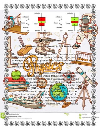
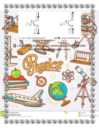
1. An introduction describing bipolar transistors and their basic operation as current-controlled current regulators.
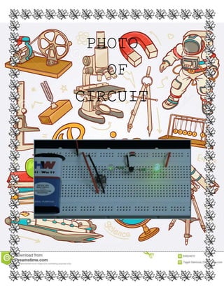
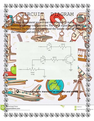
2. Details of an experiment using a transistor in a common emitter configuration with LEDs to demonstrate amplification and switching.
3. Observations made at different voltages showing the transistor acting as an amplifier when reverse biased and as a switch when forward biased.
4. Calculations verifying the current gain and voltage gain in the amplifier configuration and explaining the transistor behavior in each region.
5. A conclusion summarizing that the transistor acts as an amplifier when reverse biased in the active region