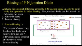
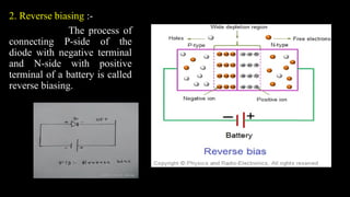
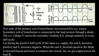
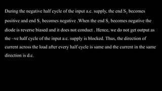
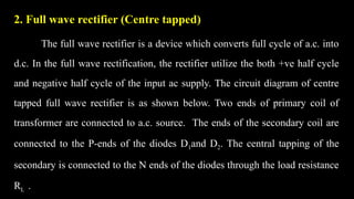
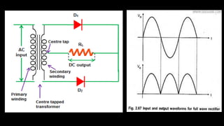
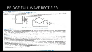
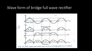
P.N. Junction
By sks (SHYAM)
P.N. Junction
If a piece of P- type semiconductor is placed in contact with a piece of N- type
semiconductor, then their exist a common contact surface between them which is
known as P- N junction.
At the junction, there is a tendency of free electron to jump from N-type to the
holes in p-type. This process is called recombination or diffusion. After some
recombination, N-region gains excess positive charge and P-region gains excess
negative charge.
These charges set up an electric field which produces a potential difference is
known as potential barrier denoted by VB. This p.d prevents further diffusion of
free electrons and holes. Inside this region, there is no mobile charge carrier so
this region is called depletion region.
P-N Junction Diode
The device in which P-type semiconductor is in contact with N-type
semiconductor is called P-N junction diode. It has two terminals namely anode
and cathode. The anode refers to the P- type region and the cathode refers to N-
type region.
Biasing of P-N junction Diode
Applying the potential difference across the P-N junction diode in order to get it
ready for operation is called biasing. The junction diode can be biased in
following two ways.
1. Forward biasing
2. Reverse biasing
1. Forward biasing : -
The process of connecting
P-side of the diode with
positive terminal and N-
side with negative terminal
of a battery is called
forward biasing.
Features:
1. Potential barrier is reduced and is eliminated at some forward voltage 0.3V to
0.7 V
2. Junction offers low resistance (forward resistance) to current.
3. Inside the diode, current is due to both type of charge carriers (i.e electrons
and holes) but outside diode it is due to flow of electrons only.
4. Depletion layer decreases.
5. Current increases with applied voltage but do not obey Ohm’s Law
2. Reverse biasing :-
The process of
connecting P-side of the
diode with negative terminal
and N-side with positive
terminal of a battery is called
reverse biasing.
In the reverse biasing , the electrons from the N-region are attracted towards the
positive terminal and holes in the P-region are attracted towards the negative
terminal of the battery. The departing electrons and holes leave more positive
ions and negative ions respectively near the junction. Therefore , the depletion
layer gets wider . The depletion layer stops growing when potential difference
across it equals the applied voltage and then free electrons and holes stop
growing. So, the flow of negligible current inside the diode is due to minority
charge carriers.
Features:
1. Potential barrier is increased.
2. Depletion layer is increased
3. The junction offers very high resistance (reverse resistance)
4. Reverse current is very small and is called leakage current.
Characteristics of a p-n junction diode
The graphical relationship between current and potential difference across
the junction diode is called characteristics of a diode. It is also known as I-V
characteristics of junction diode. Usually, the voltage is taken along x-axis and
the current along y-axis. These are of two types.
1. Forward characteristics :- fig
It is the graphical relation between forward current and forward voltage . The
circuit diagram for studying the forward characteristics of p-n junction diode is
as shown in figure.
Fig: b Forward characteristics
of PN junction diode
Fig: a Circuit diagram for
forward biasing
The voltmeter V measures the potential difference across the diode and
milliammeter mA measures the current flows through it. The forward voltage
across the diode V is changed with the help of rheostat RH and corresponding
forward current I is noted.
The forward voltage at which the current through the diode starts to increase
rapidly is called knee voltage and is denoted by Vk.
The knee voltage for silicon and germanium is .
Vk = 0.7V for silicon
Vk = 0.3V for germanium
2. Reverse characteristics
It is the graphical relation between reverse current and reverse voltage. The
circuit diagram for studying reverse characteristics is shown in fig. The
voltmeter V measures the reverse voltage and microammeter μA measures the
reverse current. A graph is then plotted between reverse voltage and reverse
current. This graph represents the reverse characteristics of the diode. The
reverse voltage at which the diode current starts to increase sharply is called
breakdown voltage vB
Fig: a Reverse biasing circuit Fig: b Reverse biasing characteristics
Rectification and rectifier
The process of conversion of a.c. into d.c. is called rectification. The device
which is used for rectification is called a rectifier. The p-n junction diode
conducts in forward bias and doesn’t conduct in reverse bias. This unidirectional
current conduction property of diode is used in rectification.
There are two types of rectifier
1. Half wave rectifier
2. Full wave rectifier
Half wave rectifier:
A rectifier which converts only half cycle of a.c. into d.c. is called half wave
rectifier. The circuit diagram of a half –wave rectifier is as shown in figure .
Two ends of the primary coil of transformer are connected to a.c. source.
Secondary coil of transformer is connected to the load resistor through a diode .
The a.c. voltage V across the secondary winding S1S2 changes polarity in every
half cycle.
Let during the positive half cycle of the input a.c. supply, the end S1 becomes
positive and S2 becomes negative. When the end S1 becomes positive the diode
is forward biased and hence it conducts the current. So, we get output across the
load R .
During the negative half cycle of the input a.c. supply, the end S2 becomes
positive and end S1 becomes negative .When the end S1 becomes negative the
diode is reverse biased and it does not conduct . Hence, we do not get output as
the –ve half cycle of the input a.c. supply is blocked. Thus, the direction of
current across the load after every half cycle is same and the current in the same
direction is d.c.
2. Full wave rectifier (Centre tapped)
The full wave rectifier is a device which converts full cycle of a.c. into
d.c. In the full wave rectification, the rectifier utilize the both +ve half cycle
and negative half cycle of the input ac supply. The circuit diagram of centre
tapped full wave rectifier is as shown below. Two ends of primary coil of
transformer are connected to a.c. source. The ends of the secondary coil are
connected to the P-ends of the diodes D1and D2. The central tapping of the
secondary is connected to the N ends of the diodes through the load resistance
RL .
As we know, the A.C voltage changes its polarity in every half cycle. During the
positive half cycle, say the end S1 becomes +ve and end S2 becomes –ve. When the
end S1 becomes +ve, the diode D1 is forward biased and D2 is reverse biased. So, the
diode D1 conduct the current and diode D2doesnot conduct. The direction of current
through the load is as shown by arrow head in the upper half of the secondary winding.
During the –ve half cycle of input a.c. supply , the end S2 becomes +ve and end S1
becomes –Ve . When the end S2 becomes +Ve the diode D2is forward biased and diode
D1is reverse biased. The diode D2 conduct the current and diode D1 doesnot conduct.
The direction of Current is shown by arrow head in the lower half of the secondary
winding. So, in both half cycle , the direction of current through the load is in the same
direction which is d.c.
In this way, by working alternately two diode utilize both half cycle of a.c. input
supply and we get d.c.
BRIDGE FULL WAVE RECTIFIER
Wave form of bridge full wave rectifier

P-N-Junction slide for class 12 neb.pptx

  • 1.
  • 2.
    P.N. Junction If apiece of P- type semiconductor is placed in contact with a piece of N- type semiconductor, then their exist a common contact surface between them which is known as P- N junction. At the junction, there is a tendency of free electron to jump from N-type to the holes in p-type. This process is called recombination or diffusion. After some recombination, N-region gains excess positive charge and P-region gains excess negative charge. These charges set up an electric field which produces a potential difference is known as potential barrier denoted by VB. This p.d prevents further diffusion of free electrons and holes. Inside this region, there is no mobile charge carrier so this region is called depletion region.
  • 4.
    P-N Junction Diode Thedevice in which P-type semiconductor is in contact with N-type semiconductor is called P-N junction diode. It has two terminals namely anode and cathode. The anode refers to the P- type region and the cathode refers to N- type region.
  • 5.
    Biasing of P-Njunction Diode Applying the potential difference across the P-N junction diode in order to get it ready for operation is called biasing. The junction diode can be biased in following two ways. 1. Forward biasing 2. Reverse biasing 1. Forward biasing : - The process of connecting P-side of the diode with positive terminal and N- side with negative terminal of a battery is called forward biasing.
  • 6.
    Features: 1. Potential barrieris reduced and is eliminated at some forward voltage 0.3V to 0.7 V 2. Junction offers low resistance (forward resistance) to current. 3. Inside the diode, current is due to both type of charge carriers (i.e electrons and holes) but outside diode it is due to flow of electrons only. 4. Depletion layer decreases. 5. Current increases with applied voltage but do not obey Ohm’s Law
  • 7.
    2. Reverse biasing:- The process of connecting P-side of the diode with negative terminal and N-side with positive terminal of a battery is called reverse biasing.
  • 8.
    In the reversebiasing , the electrons from the N-region are attracted towards the positive terminal and holes in the P-region are attracted towards the negative terminal of the battery. The departing electrons and holes leave more positive ions and negative ions respectively near the junction. Therefore , the depletion layer gets wider . The depletion layer stops growing when potential difference across it equals the applied voltage and then free electrons and holes stop growing. So, the flow of negligible current inside the diode is due to minority charge carriers. Features: 1. Potential barrier is increased. 2. Depletion layer is increased 3. The junction offers very high resistance (reverse resistance) 4. Reverse current is very small and is called leakage current.
  • 9.
    Characteristics of ap-n junction diode The graphical relationship between current and potential difference across the junction diode is called characteristics of a diode. It is also known as I-V characteristics of junction diode. Usually, the voltage is taken along x-axis and the current along y-axis. These are of two types. 1. Forward characteristics :- fig It is the graphical relation between forward current and forward voltage . The circuit diagram for studying the forward characteristics of p-n junction diode is as shown in figure.
  • 10.
    Fig: b Forwardcharacteristics of PN junction diode Fig: a Circuit diagram for forward biasing
  • 11.
    The voltmeter Vmeasures the potential difference across the diode and milliammeter mA measures the current flows through it. The forward voltage across the diode V is changed with the help of rheostat RH and corresponding forward current I is noted. The forward voltage at which the current through the diode starts to increase rapidly is called knee voltage and is denoted by Vk. The knee voltage for silicon and germanium is . Vk = 0.7V for silicon Vk = 0.3V for germanium
  • 12.
    2. Reverse characteristics Itis the graphical relation between reverse current and reverse voltage. The circuit diagram for studying reverse characteristics is shown in fig. The voltmeter V measures the reverse voltage and microammeter μA measures the reverse current. A graph is then plotted between reverse voltage and reverse current. This graph represents the reverse characteristics of the diode. The reverse voltage at which the diode current starts to increase sharply is called breakdown voltage vB Fig: a Reverse biasing circuit Fig: b Reverse biasing characteristics
  • 13.
    Rectification and rectifier Theprocess of conversion of a.c. into d.c. is called rectification. The device which is used for rectification is called a rectifier. The p-n junction diode conducts in forward bias and doesn’t conduct in reverse bias. This unidirectional current conduction property of diode is used in rectification. There are two types of rectifier 1. Half wave rectifier 2. Full wave rectifier Half wave rectifier: A rectifier which converts only half cycle of a.c. into d.c. is called half wave rectifier. The circuit diagram of a half –wave rectifier is as shown in figure .
  • 14.
    Two ends ofthe primary coil of transformer are connected to a.c. source. Secondary coil of transformer is connected to the load resistor through a diode . The a.c. voltage V across the secondary winding S1S2 changes polarity in every half cycle. Let during the positive half cycle of the input a.c. supply, the end S1 becomes positive and S2 becomes negative. When the end S1 becomes positive the diode is forward biased and hence it conducts the current. So, we get output across the load R .
  • 15.
    During the negativehalf cycle of the input a.c. supply, the end S2 becomes positive and end S1 becomes negative .When the end S1 becomes negative the diode is reverse biased and it does not conduct . Hence, we do not get output as the –ve half cycle of the input a.c. supply is blocked. Thus, the direction of current across the load after every half cycle is same and the current in the same direction is d.c.
  • 16.
    2. Full waverectifier (Centre tapped) The full wave rectifier is a device which converts full cycle of a.c. into d.c. In the full wave rectification, the rectifier utilize the both +ve half cycle and negative half cycle of the input ac supply. The circuit diagram of centre tapped full wave rectifier is as shown below. Two ends of primary coil of transformer are connected to a.c. source. The ends of the secondary coil are connected to the P-ends of the diodes D1and D2. The central tapping of the secondary is connected to the N ends of the diodes through the load resistance RL .
  • 18.
    As we know,the A.C voltage changes its polarity in every half cycle. During the positive half cycle, say the end S1 becomes +ve and end S2 becomes –ve. When the end S1 becomes +ve, the diode D1 is forward biased and D2 is reverse biased. So, the diode D1 conduct the current and diode D2doesnot conduct. The direction of current through the load is as shown by arrow head in the upper half of the secondary winding. During the –ve half cycle of input a.c. supply , the end S2 becomes +ve and end S1 becomes –Ve . When the end S2 becomes +Ve the diode D2is forward biased and diode D1is reverse biased. The diode D2 conduct the current and diode D1 doesnot conduct. The direction of Current is shown by arrow head in the lower half of the secondary winding. So, in both half cycle , the direction of current through the load is in the same direction which is d.c. In this way, by working alternately two diode utilize both half cycle of a.c. input supply and we get d.c.
  • 19.
  • 20.
    Wave form ofbridge full wave rectifier