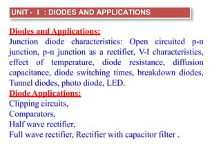
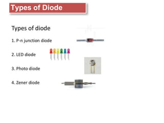
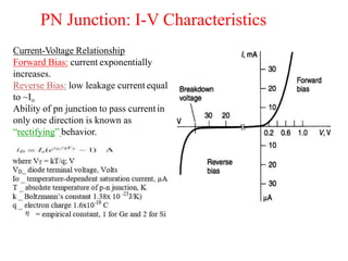
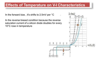
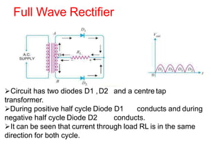
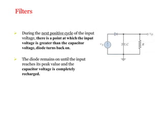
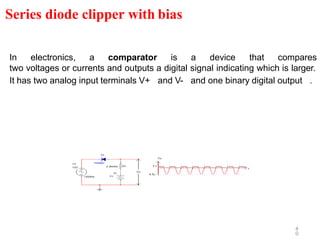
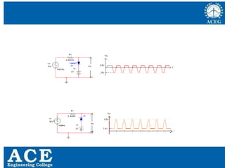
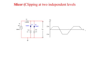
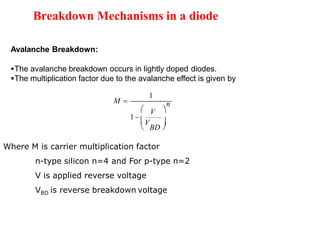
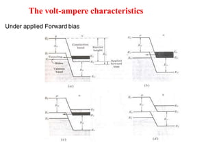
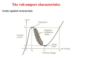
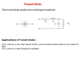
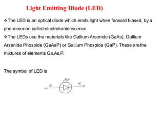
SlideShare a Scribd company logo
1 of 66
ANALOG & DIGITALELECTRONICS
by
Kumar Saliganti
Assistant Professor (C)
skjntum@gmail.com
Department of Electrical and Electronics Engineering
JNTUH University College of Engineering Manthani
SYLLABUS:
I : Diodes andApplications
II : BJTs
IV : FETs and Digital Circuits
III : Combinational Logic Circuits
UNIT -
UNIT –
UNIT –
UNIT –
UNIT – V : Sequential Logic Circuits
P
.KIRAN KUMAR,ECE DEPARTMENT
Circuits and
•Integrated Electronics: Analog and Digital
Systems, 2/e, Jaccob Millman,
Christos Halkias and Chethan D. Parikh, Tata
McGraw-Hill Education, India, 2010.
•Digital Design, 5/e, Morris Mano and Michael
D. Cilette, Pearson, 2011
TEXTBOOKS:
UNIT - I : DIODES AND APPLICATIONS
Diodes andApplications:
Junction diode characteristics: Open circuited p-n
junction, p-n junction as a rectifier, V-I characteristics,
effect of temperature, diode resistance, diffusion
capacitance, diode switching times, breakdown diodes,
Tunnel diodes, photo diode, LED.
DiodeApplications:
Clipping circuits,
Comparators,
Half wave rectifier,
Full wave rectifier, Rectifier with capacitor filter .
A Diode is the simplest two-terminal electronic
device. It allows current to flow only in one direction and
blocks the current that flows in the opposite direction.
The two terminals of the diode are called as anode
(+) and cathode (-).
DIODE
A K
Symbol of a Diode
The name diode is derived from “Di–Ode”
which means a device that has two electrodes.
Di – means Two (2)
Ode – means Electrodes
Diode: “Di – Ode”
Formation of a Diode
If a P-type and an N-type material are brought close to each
other, both of them join to form a junction.
As shown in the figure below.
P-type material has holes as the majority carriers and
an N-type material has electrons as the majority carriers.
As opposite charges attract, few holes in P-type tend to go
toN-side, whereas few electrons in N-type tend to go to P-
side.
As both of them travel towards the junction, holes and
electrons recombine with each other to neutralize and forms
ions.
Now, in this junction, there exists a region where the
positive and negative ions are formed, called as PN junction
or junction barrier
Diode’s Three Operation Regions
• In order to understand the operation of a
diode, it is necessary to study its three
operation regions: equilibrium, reverse
bias, and forward bias.
The formation of negative ions on P-side and
positive ions on N-side results in the formation of a
narrow charged region on either side of the PN
junction. This region is now free from movable
charge carriers.
The ions present here have been stationary and
maintain a region of space between them
without any charge carriers. As this region acts
as a barrier between P and N type materials, this
is also called as Barrier junction. This has
another name called as Depletion region
meaning it depletes both the regions.
Types of Diode
The PN junction diode is a two terminal device, which is
formed when one side of the PN junction diode is made
with p-type and doped with the N-type material.
Forward & Reverse Biased
Current-Voltage Relationship
Forward Bias: current exponentially
increases.
Reverse Bias: low leakage current equal
to ~Io
Ability of pn junction to pass currentin
only one direction is known as
“rectifying” behavior.
PN Junction: I-V Characteristics
In the forward bias , it's shifts to 2.5mV per °C
In the reverse biased condition because the reverse
saturation current of a silicon diode doubles for every
10°C rose in temperature
Effects of Temperature on V-I Characteristics
Diode resistance
Static Resistance or (DC resistance)
Forward Resistance Rf
Reverse Resistance Rr
Dynamic Resistance or (AC resistance)
Forward Resistance rf
Reverse Resistance rr
Diode resistance
• ΔV/ΔI is called ac (dynamic) resistance of the diode because
we
consider small change in voltage
• We would not want to calculate ac resistance between
V=0.55V and V=0.65V
• rd= ΔV/ΔI ohms
• The dc resistance of a diode is found by dividing the dc
voltage across it by dc current through it. DC resistance also
called the static resistance.
Rd=V/I ohms
• Diode is nonlinear in both the dc & the ac sense, that is, both
its dc
& ac resistance change over a wide range.
AC & DC Resistance
V (V)
I (mA)
0 0.1 0.2 0.3 0.4 0.5 0.6
0
40
10
20
30
ΔI
ΔV
rD = ΔV / ΔI
AC Resistance
DC Resistance
RD = V /I
rD = VT / I
Diode capacitance
•Transition capacitance (CT)
The change of capacitance at the depletion
region can be defined as the change in
electric charge per change in voltage.
CT = dQ / dV
C = ε A /W
Where,
CT = Transition capacitance
dQ = Change in electric charge
dV = Change in voltage
The transition capacitance can be
mathematically written as,
,
•Diffusion capacitance or Storage capacitance (CD)
•CD is due to the storage of minority
carriers in a forward biased diode
•It will dominate in the device only during
high frequency operation
•CD>CT
Switching characteristics of pn junction diode
The sudden change from forward to reverse and from reverse to forward bias, affects
the circuit. The time taken to respond to such sudden changes is the important criterion
to define the effectiveness of an electrical switch.
•The time taken before the diode recovers its steady state is called as Recovery
Time.(trr)
•The time interval taken by the diode to switch from reverse biased state to forward
biased state is called as Forward Recovery Time.
•The time interval taken by the diode to switch from forward biased state to reverse
biased state is called as Reverse Recovery Time.
Storage time − The time period for which the diode remains in the conduction
state even in the reverse biased state, is called as Storage time.
Transition time − The time elapsed in returning back to the state of non-
conduction, i.e. steady state reverse bias, is called Transition time.
Reverse recovery time (trr)= Storage time(Ts)+Transition time (Tt)
Ideal vs practical diode
Block diagram of a Power Supply
Rectifiers
• Rectifier is a device which convert
AC voltage in to pulsating DC
• A rectifier utilizes unidirectional
conducting device
• Ex :P-N junction diodes
Type
s
• Depending up on the period of
conduction
 Half wave rectifier
 Full wave rectifier
• Depending up on the connection
procedure
Bridge rectifier
Half wave
Rectifier
• The process of removing one-half the input signalto
establish a dc level is called half-waverectification.
• In Half wave rectification, the rectifier conductscurrent
during positive half cycle of input ac signalonly.
• Negative half cycle is suppressed.
Full Wave Rectifier
and a centre tap
Circuit has two diodes D1 ,D2
transformer.
During positive half cycle Diode D1 conducts and during
negative half cycle Diode D2 conducts.
It can be seen that current through load RL is in the same
direction for both cycle.
Full Wave Bridge
Rectifier
Need for centre tapped PT is eliminated.
Consists of 4 diodes instead of 2.
Full Wave Bridge
Rectifier
During period t=0 to t=T/2 D2 and
D3 are conducting while D1 and D4
are in the “off” state.
During period t=T/2 to t=T D1 and D4 are
conducting while D2 and D3 are in the “off”
state.
Filters
 Acapacitor is added in parallel with the
load resistor of a half-wave rectifier to
form a simple filter circuit. At first there
is no charge across the capacitor
 During the 1st quarter positive
cycle, diode is forward biased, and C
charges up.
 VC= VO= VS- V.
 As VSfalls back towards zero, and
into the negative cycle, the
capacitor discharges through the
resistor R.The diode is reversed
biased ( turnedoff)
 Ifthe RCtime constant is large, the
voltage across the capacitor
discharges exponentially.
Filters
 During the next positive cycle of the input
voltage, there is a point at which the input
voltage is greater than the capacitor
voltage, diode turns back on.
 The diode remains on until the input
reaches its peak value and the
capacitor voltage is completely
recharged.
Quarter cycle;
capacitor
charges up
Capacitor discharges
through Rsince diode
becomes off
Input voltage is greater
than the capacitor
voltage; recharge before
discharging again
VC= Vme – t / RC
NOTE:Vmis the peak value of the capacitor voltage = VP- V
Since the capacitor filters out a large portion of the sinusoidal signal, it is calleda
filtercapacitor.
Vp
Vm
P
.KIRAN KUMAR,ECE DEPARTMENT
3
Figure: Half-wave rectifier with smoothing capacitor.
Ripple Voltage, and Diode Current
Vr= ripple voltage
Vr = VM –VMe-T’/RC
where T’ = time of the
capacitor to discharge toits
lowest value
Vr= VM( 1 –e-T’/RC )
Expand the exponential in
series,
Vr= (VMT’) / RC
T’
Tp
• Ifthe ripple is very small, we can approximate T’ = Tp
which is the period of the inputsignal
• Hence for half wave rectifier
Vr= ( VMTp) / RC
 For full wave rectifier
Vr= ( VM0.5Tp) /RC
DIODECLIPPERS
Clipping circuits basically limit the amplitude of the input signal either below or
above certain voltage level. They are referred to as Voltage limiters, Amplitude
selectors or Slicers. A clipping circuit is one, in which a small section of input
waveform is missing or cut or truncated at the out putsection.
Clipping circuits are classified based on the position of Diode.
1.Series Diode Clipper
2.Shunt Diode Clipper
Series Diode clippers
Shunt diode clippers
4
0
In electronics, a comparator is a device that compares
two voltages or currents and outputs a digital signal indicating which is larger.
It has two analog input terminals V+ and V- and one binary digital output .
Series diode clipper with bias
P.KIRAN KUMAR,ECE
DEPARTMENT
41
Slicer (Clipping at two independent levels)
Diode equivalent circuits / models:
Applications
There are many applications in which diode switching circuits are used, such as −
Breakdown Mechanisms in a diode
When reverse voltage increases beyond certain value, large diode
current flows, this is called breakdown of diode, and corresponding
voltage is called reverse breakdown voltage of diode.
There are two distinct mechanisms due to which the break down may
occur in the diode, these are:
•Avalanche breakdown
•Zener break down
Breakdown Mechanisms in a diode
Avalanche Breakdown:
The avalanche breakdown occurs in lightly doped diodes.
The multiplication factor due to the avalanche effect is given by
1
n
V
M 
 
1
V 
 BD 
Where M is carrier multiplication factor
n-type silicon n=4 and For p-type n=2
V is applied reverse voltage
VBD is reverse breakdown voltage
Breakdown Mechanisms in a diode
Zener Breakdown
•The zener breakdown occurs in heavily doped diodes.
•For heavily doped diodes, the depletion region width is small.
•Under reverse bias conditions, the electric field across the depletion layer is very
intense. Breaking of covalent bonds due to intense electric field across the narrow
depletion region and generating large number of electrons is called Zener effect.
•These generated electrons constitute a very large current and the mechanism is
called Zener breakdown.
•The diodes having reverse breakdown voltage less than 5v shows the Zener
mechanism of breakdown.
Zener Diode
•Zener diode is a heavily doped diode, and is designed with adequate power
dissipation capabilities to operate in the reverse breakdown region.
•The operation of the zener diode is same as that of ordinary PN diode under
forward biased condition.
•In reverse biased condition, the diode carries reverse saturation current, till the
reverse voltage applied is less than the reverse breakdown voltage.
•When the reverse voltage exceeds the reverse breakdown voltage, the current
through it changes drastically but the voltage across it remains almost constant such
a break down region is a normal operating region for a zener diode.
The symbol of zener diode is
Zener Diode
The dynamic resistance of a zener diode is
defined as the reciprocal of the slope of the
reverse characteristics in zener region.
rz 
Vz
Iz
= 1 / slope of reverse
characteristics in zener region
•The dynamic resistance is very small, it is of he order of few tens of ohms.
Equivalent circuit of Zener diode
Applications of zener diode
The various applications of zener diode are,
•As a voltage regulating element in voltage regulators.
•In various protecting circuits.
•In zener limiters i.e., clipping circuits which are used to clip off the unwanted
portion of the voltage waveform.
Tunnel diode
•If the concentration of impurity atoms is greatly increased, say 1 part in 103
the device characteristics are completely changed.
•The new diode was announced in 1958 by Leo Esaki. This diode is called
‘Tunnel diode’ or ‘Esaki diode’.
•The barrier potential VB is related with the width of the depletion region with
the following equation.
•From the above equation the width of the barrier varies inversely as the
square root of impurity concentration.
•As the depletion width decreases there is a large probability that an electron
will penetrate through the barrier. This quantum mechanical behavior is
referred to as tunneling and hence these high impurity density pn-junction
devices are called Tunnel diodes.
B
q NA
V  .²
2 q NA
2VB 
.
 ² 
Tunnel diode
Energy band structure of heavily doped pn-junction diode under open
circuited conditions
The volt-ampere characteristics
Under applied reverse bias
The volt-ampere characteristics
Under applied Forward bias
The volt-ampere characteristics
Under applied reverse bias
Tunnel diode
The tunnel diode symbol and small-signal model are
Applications of Tunnel diode:
•It is used as a very high speed switch, since tunneling takes place at the speed of
light.
•It is used as a high frequency oscillator.
Photodiode
•The photodiode is a device that operates in reverse diode.
•The photodiode has a small transparent window that allows light to strike
one surface of the pn-junction, keeping the remaining sides unilluminated.
The symbol of photodiode is
The volt-ampere characteristics of photodiode
Photodiode
Advantages of Photo diodes:
•It can be used as variable-resistance device.
•Highly sensitive to the light.
•The speed of operation is very high.
Disadvantages of Photo diodes:
The dark current is temperature dependent.
Applications of photodiode:
Photodiodes are commonly used in alarm systems and counting systems.
Used in demodulators.
Used in encoders.
Used in light detectors.
Used in optical communication systems.
Light Emitting Diode (LED)
The LED is an optical diode which emits light when forward biased, by a
phenomenon called electroluminescence.
The LEDs use the materials like Gallium Arsenide (GaAs), Gallium
Arsenide Phospide (GaAsP) or Gallium Phospide (GaP). These arethe
mixtures of elements Ga,As,P.
The symbol of LED is
LED Working Principle
•When an LED is forward biased, the electrons and holes move towards the
junction and recombination takes place.
• As a result of recombination, the electrons lying in the conduction bands of
n-region fall into the holes lying in the valance band of p-region.
•The difference of energy between the conduction band and the valance
band is radiated in the form of light energy.
•The energy released in the form of light depends on the energy
corresponding to the forbidden gap. This determines the wavelength of the
emitted light.
•The wavelength determines the color of the light and also determines
whether the light is visible or invisible (infrared).
LED Working Principle
•The color of the emitted light depends on the type of material used.
Gallium Arsenide (GaAs) --- Infrared radiation(invisible)
Gallium Phospide (GaP) --- Red or Green
Gallium Arsenide Phospide (GaAsP) --- Red orYellow.
•The brightness of the emitted light is directly proportional to the forward
bias current.
Output characteristics of LED
Process of electro luminescence
Typical output characteristics for LED
Light Emitting Diode (LED)
Advantages of LEDs:
• LEDs are small in size.
•LEDs are fast operating devices.
•LEDs are light in weight.
•LEDs are available in various colors.
•The LEDs have long life.
•The LEDs are cheap and readily available.
•LEDs are easy to interface with various other electronic circuits.
Disadvantages of LEDs:
• Needs large power for the operation.
•The characteristics are affected by the temperature.
Light Emitting Diode (LED)
Applications of LEDs:
•The LEDs are used in all kinds of visual displays i.e., seven
segment displays and alpha numeric displays. Such displays
are commonly used in multimeter, calculator, watches etc.
•LEDs are also used in optical devices such as optocouplers.
They are also used in burglar alarm systems.

More Related Content

Similar to ADE UNIT-I.pptx

1st year basic electronics
1st year basic electronics1st year basic electronics
1st year basic electronicssaifam
 
PE4MSc_Ch1_SC_devices.pptx
PE4MSc_Ch1_SC_devices.pptxPE4MSc_Ch1_SC_devices.pptx
PE4MSc_Ch1_SC_devices.pptxAddisuMengesha2
 
ELL PROJECT.pdf
ELL PROJECT.pdfELL PROJECT.pdf
ELL PROJECT.pdfSuiaj
 
Rectifier and Filter circuits (chapter14)
Rectifier and Filter circuits (chapter14)Rectifier and Filter circuits (chapter14)
Rectifier and Filter circuits (chapter14)DHARUN MUGHILAN
 
Type of pn junction & rectifiers plus Transistor
Type of pn junction & rectifiers plus TransistorType of pn junction & rectifiers plus Transistor
Type of pn junction & rectifiers plus TransistorMuhammad Adeel Shakir
 
adeunit1-221223065954-a64adaae.pdf
adeunit1-221223065954-a64adaae.pdfadeunit1-221223065954-a64adaae.pdf
adeunit1-221223065954-a64adaae.pdfKUMARS641064
 
377275109-Ch-2-Uncontrolled-Rectifiers-Autosaved.pptx
377275109-Ch-2-Uncontrolled-Rectifiers-Autosaved.pptx377275109-Ch-2-Uncontrolled-Rectifiers-Autosaved.pptx
377275109-Ch-2-Uncontrolled-Rectifiers-Autosaved.pptxpriyakunduq
 
EC8252-Electronic Devices Question Bank.pdf
EC8252-Electronic Devices Question Bank.pdfEC8252-Electronic Devices Question Bank.pdf
EC8252-Electronic Devices Question Bank.pdfRajaSekaran923497
 
Halfwave and full wave rectificaton
Halfwave and full wave rectificaton Halfwave and full wave rectificaton
Halfwave and full wave rectificaton University of Karachi
 
Analog Electronics - Basics - Part-1
Analog Electronics - Basics - Part-1Analog Electronics - Basics - Part-1
Analog Electronics - Basics - Part-1MEENAKSHISUNDARAVELS
 
Ch2-Diode.for electrical and computer engineering
Ch2-Diode.for electrical and computer engineeringCh2-Diode.for electrical and computer engineering
Ch2-Diode.for electrical and computer engineeringabdiihuseen31
 
Full Wave Rectifier (FWR) Microproject
Full Wave Rectifier (FWR) MicroprojectFull Wave Rectifier (FWR) Microproject
Full Wave Rectifier (FWR) MicroprojectOmprakash Chauhan
 

Similar to ADE UNIT-I.pptx (20)

1st year basic electronics
1st year basic electronics1st year basic electronics
1st year basic electronics
 
UNIT_5 PPT-MBM.pptx
UNIT_5 PPT-MBM.pptxUNIT_5 PPT-MBM.pptx
UNIT_5 PPT-MBM.pptx
 
PE4MSc_Ch1_SC_devices.pptx
PE4MSc_Ch1_SC_devices.pptxPE4MSc_Ch1_SC_devices.pptx
PE4MSc_Ch1_SC_devices.pptx
 
ELL PROJECT.pdf
ELL PROJECT.pdfELL PROJECT.pdf
ELL PROJECT.pdf
 
Edcqnaunit 8
Edcqnaunit 8Edcqnaunit 8
Edcqnaunit 8
 
Rectifier and Filter circuits (chapter14)
Rectifier and Filter circuits (chapter14)Rectifier and Filter circuits (chapter14)
Rectifier and Filter circuits (chapter14)
 
Eg1108 rectifiers
Eg1108 rectifiersEg1108 rectifiers
Eg1108 rectifiers
 
Type of pn junction & rectifiers plus Transistor
Type of pn junction & rectifiers plus TransistorType of pn junction & rectifiers plus Transistor
Type of pn junction & rectifiers plus Transistor
 
ADE Unit1.pptx
ADE Unit1.pptxADE Unit1.pptx
ADE Unit1.pptx
 
adeunit1-221223065954-a64adaae.pdf
adeunit1-221223065954-a64adaae.pdfadeunit1-221223065954-a64adaae.pdf
adeunit1-221223065954-a64adaae.pdf
 
377275109-Ch-2-Uncontrolled-Rectifiers-Autosaved.pptx
377275109-Ch-2-Uncontrolled-Rectifiers-Autosaved.pptx377275109-Ch-2-Uncontrolled-Rectifiers-Autosaved.pptx
377275109-Ch-2-Uncontrolled-Rectifiers-Autosaved.pptx
 
EC8252-Electronic Devices Question Bank.pdf
EC8252-Electronic Devices Question Bank.pdfEC8252-Electronic Devices Question Bank.pdf
EC8252-Electronic Devices Question Bank.pdf
 
Halfwave and full wave rectificaton
Halfwave and full wave rectificaton Halfwave and full wave rectificaton
Halfwave and full wave rectificaton
 
Special diodes.ppt
Special diodes.pptSpecial diodes.ppt
Special diodes.ppt
 
EMI-tansducers
EMI-tansducersEMI-tansducers
EMI-tansducers
 
power electronics
power electronicspower electronics
power electronics
 
Diode Applications.pptx
Diode Applications.pptxDiode Applications.pptx
Diode Applications.pptx
 
Analog Electronics - Basics - Part-1
Analog Electronics - Basics - Part-1Analog Electronics - Basics - Part-1
Analog Electronics - Basics - Part-1
 
Ch2-Diode.for electrical and computer engineering
Ch2-Diode.for electrical and computer engineeringCh2-Diode.for electrical and computer engineering
Ch2-Diode.for electrical and computer engineering
 
Full Wave Rectifier (FWR) Microproject
Full Wave Rectifier (FWR) MicroprojectFull Wave Rectifier (FWR) Microproject
Full Wave Rectifier (FWR) Microproject
 

More from KUMARS641064

introduction-power-systems-08-aa (2).ppt
introduction-power-systems-08-aa (2).pptintroduction-power-systems-08-aa (2).ppt
introduction-power-systems-08-aa (2).pptKUMARS641064
 
Energy Generation.ppt
Energy Generation.pptEnergy Generation.ppt
Energy Generation.pptKUMARS641064
 
ADE UNIT-III (Digital Fundamentals).pptx
ADE UNIT-III (Digital Fundamentals).pptxADE UNIT-III (Digital Fundamentals).pptx
ADE UNIT-III (Digital Fundamentals).pptxKUMARS641064
 
addeunit-2-191121144848.pptx
addeunit-2-191121144848.pptxaddeunit-2-191121144848.pptx
addeunit-2-191121144848.pptxKUMARS641064
 
Half-wave-rectifier.pdf
Half-wave-rectifier.pdfHalf-wave-rectifier.pdf
Half-wave-rectifier.pdfKUMARS641064
 
DC MOTORS-UNIT-II.pdf
DC MOTORS-UNIT-II.pdfDC MOTORS-UNIT-II.pdf
DC MOTORS-UNIT-II.pdfKUMARS641064
 

More from KUMARS641064 (9)

introduction-power-systems-08-aa (2).ppt
introduction-power-systems-08-aa (2).pptintroduction-power-systems-08-aa (2).ppt
introduction-power-systems-08-aa (2).ppt
 
Energy Generation.ppt
Energy Generation.pptEnergy Generation.ppt
Energy Generation.ppt
 
ADE UNIT-2.pptx
ADE UNIT-2.pptxADE UNIT-2.pptx
ADE UNIT-2.pptx
 
ADE UNIT-III (Digital Fundamentals).pptx
ADE UNIT-III (Digital Fundamentals).pptxADE UNIT-III (Digital Fundamentals).pptx
ADE UNIT-III (Digital Fundamentals).pptx
 
Lecture17.ppt
Lecture17.pptLecture17.ppt
Lecture17.ppt
 
SpecialDiodes.pdf
SpecialDiodes.pdfSpecialDiodes.pdf
SpecialDiodes.pdf
 
addeunit-2-191121144848.pptx
addeunit-2-191121144848.pptxaddeunit-2-191121144848.pptx
addeunit-2-191121144848.pptx
 
Half-wave-rectifier.pdf
Half-wave-rectifier.pdfHalf-wave-rectifier.pdf
Half-wave-rectifier.pdf
 
DC MOTORS-UNIT-II.pdf
DC MOTORS-UNIT-II.pdfDC MOTORS-UNIT-II.pdf
DC MOTORS-UNIT-II.pdf
 

Recently uploaded

Solving Puzzles Benefits Everyone (English).pptx
Solving Puzzles Benefits Everyone (English).pptxSolving Puzzles Benefits Everyone (English).pptx
Solving Puzzles Benefits Everyone (English).pptxOH TEIK BIN
 
The basics of sentences session 2pptx copy.pptx
The basics of sentences session 2pptx copy.pptxThe basics of sentences session 2pptx copy.pptx
The basics of sentences session 2pptx copy.pptxheathfieldcps1
 
APM Welcome, APM North West Network Conference, Synergies Across Sectors
APM Welcome, APM North West Network Conference, Synergies Across SectorsAPM Welcome, APM North West Network Conference, Synergies Across Sectors
APM Welcome, APM North West Network Conference, Synergies Across SectorsAssociation for Project Management
 
PSYCHIATRIC History collection FORMAT.pptx
PSYCHIATRIC   History collection FORMAT.pptxPSYCHIATRIC   History collection FORMAT.pptx
PSYCHIATRIC History collection FORMAT.pptxPoojaSen20
 
MENTAL STATUS EXAMINATION format.docx
MENTAL     STATUS EXAMINATION format.docxMENTAL     STATUS EXAMINATION format.docx
MENTAL STATUS EXAMINATION format.docxPoojaSen20
 
Employee wellbeing at the workplace.pptx
Employee wellbeing at the workplace.pptxEmployee wellbeing at the workplace.pptx
Employee wellbeing at the workplace.pptxNirmalaLoungPoorunde1
 
Grant Readiness 101 TechSoup and Remy Consulting
Grant Readiness 101 TechSoup and Remy ConsultingGrant Readiness 101 TechSoup and Remy Consulting
Grant Readiness 101 TechSoup and Remy ConsultingTechSoup
 
Mastering the Unannounced Regulatory Inspection
Mastering the Unannounced Regulatory InspectionMastering the Unannounced Regulatory Inspection
Mastering the Unannounced Regulatory InspectionSafetyChain Software
 
Separation of Lanthanides/ Lanthanides and Actinides
Separation of Lanthanides/ Lanthanides and ActinidesSeparation of Lanthanides/ Lanthanides and Actinides
Separation of Lanthanides/ Lanthanides and ActinidesFatimaKhan178732
 
SOCIAL AND HISTORICAL CONTEXT - LFTVD.pptx
SOCIAL AND HISTORICAL CONTEXT - LFTVD.pptxSOCIAL AND HISTORICAL CONTEXT - LFTVD.pptx
SOCIAL AND HISTORICAL CONTEXT - LFTVD.pptxiammrhaywood
 
A Critique of the Proposed National Education Policy Reform
A Critique of the Proposed National Education Policy ReformA Critique of the Proposed National Education Policy Reform
A Critique of the Proposed National Education Policy ReformChameera Dedduwage
 
mini mental status format.docx
mini    mental       status     format.docxmini    mental       status     format.docx
mini mental status format.docxPoojaSen20
 
Paris 2024 Olympic Geographies - an activity
Paris 2024 Olympic Geographies - an activityParis 2024 Olympic Geographies - an activity
Paris 2024 Olympic Geographies - an activityGeoBlogs
 
“Oh GOSH! Reflecting on Hackteria's Collaborative Practices in a Global Do-It...
“Oh GOSH! Reflecting on Hackteria's Collaborative Practices in a Global Do-It...“Oh GOSH! Reflecting on Hackteria's Collaborative Practices in a Global Do-It...
“Oh GOSH! Reflecting on Hackteria's Collaborative Practices in a Global Do-It...Marc Dusseiller Dusjagr
 
Call Girls in Dwarka Mor Delhi Contact Us 9654467111
Call Girls in Dwarka Mor Delhi Contact Us 9654467111Call Girls in Dwarka Mor Delhi Contact Us 9654467111
Call Girls in Dwarka Mor Delhi Contact Us 9654467111Sapana Sha
 
Alper Gobel In Media Res Media Component
Alper Gobel In Media Res Media ComponentAlper Gobel In Media Res Media Component
Alper Gobel In Media Res Media ComponentInMediaRes1
 
Crayon Activity Handout For the Crayon A
Crayon Activity Handout For the Crayon ACrayon Activity Handout For the Crayon A
Crayon Activity Handout For the Crayon AUnboundStockton
 
Industrial Policy - 1948, 1956, 1973, 1977, 1980, 1991
Industrial Policy - 1948, 1956, 1973, 1977, 1980, 1991Industrial Policy - 1948, 1956, 1973, 1977, 1980, 1991
Industrial Policy - 1948, 1956, 1973, 1977, 1980, 1991RKavithamani
 
How to Make a Pirate ship Primary Education.pptx
How to Make a Pirate ship Primary Education.pptxHow to Make a Pirate ship Primary Education.pptx
How to Make a Pirate ship Primary Education.pptxmanuelaromero2013
 

Recently uploaded (20)

Solving Puzzles Benefits Everyone (English).pptx
Solving Puzzles Benefits Everyone (English).pptxSolving Puzzles Benefits Everyone (English).pptx
Solving Puzzles Benefits Everyone (English).pptx
 
The basics of sentences session 2pptx copy.pptx
The basics of sentences session 2pptx copy.pptxThe basics of sentences session 2pptx copy.pptx
The basics of sentences session 2pptx copy.pptx
 
APM Welcome, APM North West Network Conference, Synergies Across Sectors
APM Welcome, APM North West Network Conference, Synergies Across SectorsAPM Welcome, APM North West Network Conference, Synergies Across Sectors
APM Welcome, APM North West Network Conference, Synergies Across Sectors
 
PSYCHIATRIC History collection FORMAT.pptx
PSYCHIATRIC   History collection FORMAT.pptxPSYCHIATRIC   History collection FORMAT.pptx
PSYCHIATRIC History collection FORMAT.pptx
 
MENTAL STATUS EXAMINATION format.docx
MENTAL     STATUS EXAMINATION format.docxMENTAL     STATUS EXAMINATION format.docx
MENTAL STATUS EXAMINATION format.docx
 
Employee wellbeing at the workplace.pptx
Employee wellbeing at the workplace.pptxEmployee wellbeing at the workplace.pptx
Employee wellbeing at the workplace.pptx
 
Grant Readiness 101 TechSoup and Remy Consulting
Grant Readiness 101 TechSoup and Remy ConsultingGrant Readiness 101 TechSoup and Remy Consulting
Grant Readiness 101 TechSoup and Remy Consulting
 
Mastering the Unannounced Regulatory Inspection
Mastering the Unannounced Regulatory InspectionMastering the Unannounced Regulatory Inspection
Mastering the Unannounced Regulatory Inspection
 
Separation of Lanthanides/ Lanthanides and Actinides
Separation of Lanthanides/ Lanthanides and ActinidesSeparation of Lanthanides/ Lanthanides and Actinides
Separation of Lanthanides/ Lanthanides and Actinides
 
Model Call Girl in Bikash Puri Delhi reach out to us at 🔝9953056974🔝
Model Call Girl in Bikash Puri  Delhi reach out to us at 🔝9953056974🔝Model Call Girl in Bikash Puri  Delhi reach out to us at 🔝9953056974🔝
Model Call Girl in Bikash Puri Delhi reach out to us at 🔝9953056974🔝
 
SOCIAL AND HISTORICAL CONTEXT - LFTVD.pptx
SOCIAL AND HISTORICAL CONTEXT - LFTVD.pptxSOCIAL AND HISTORICAL CONTEXT - LFTVD.pptx
SOCIAL AND HISTORICAL CONTEXT - LFTVD.pptx
 
A Critique of the Proposed National Education Policy Reform
A Critique of the Proposed National Education Policy ReformA Critique of the Proposed National Education Policy Reform
A Critique of the Proposed National Education Policy Reform
 
mini mental status format.docx
mini    mental       status     format.docxmini    mental       status     format.docx
mini mental status format.docx
 
Paris 2024 Olympic Geographies - an activity
Paris 2024 Olympic Geographies - an activityParis 2024 Olympic Geographies - an activity
Paris 2024 Olympic Geographies - an activity
 
“Oh GOSH! Reflecting on Hackteria's Collaborative Practices in a Global Do-It...
“Oh GOSH! Reflecting on Hackteria's Collaborative Practices in a Global Do-It...“Oh GOSH! Reflecting on Hackteria's Collaborative Practices in a Global Do-It...
“Oh GOSH! Reflecting on Hackteria's Collaborative Practices in a Global Do-It...
 
Call Girls in Dwarka Mor Delhi Contact Us 9654467111
Call Girls in Dwarka Mor Delhi Contact Us 9654467111Call Girls in Dwarka Mor Delhi Contact Us 9654467111
Call Girls in Dwarka Mor Delhi Contact Us 9654467111
 
Alper Gobel In Media Res Media Component
Alper Gobel In Media Res Media ComponentAlper Gobel In Media Res Media Component
Alper Gobel In Media Res Media Component
 
Crayon Activity Handout For the Crayon A
Crayon Activity Handout For the Crayon ACrayon Activity Handout For the Crayon A
Crayon Activity Handout For the Crayon A
 
Industrial Policy - 1948, 1956, 1973, 1977, 1980, 1991
Industrial Policy - 1948, 1956, 1973, 1977, 1980, 1991Industrial Policy - 1948, 1956, 1973, 1977, 1980, 1991
Industrial Policy - 1948, 1956, 1973, 1977, 1980, 1991
 
How to Make a Pirate ship Primary Education.pptx
How to Make a Pirate ship Primary Education.pptxHow to Make a Pirate ship Primary Education.pptx
How to Make a Pirate ship Primary Education.pptx
 

ADE UNIT-I.pptx

  • 1. ANALOG & DIGITALELECTRONICS by Kumar Saliganti Assistant Professor (C) skjntum@gmail.com Department of Electrical and Electronics Engineering JNTUH University College of Engineering Manthani
  • 2. SYLLABUS: I : Diodes andApplications II : BJTs IV : FETs and Digital Circuits III : Combinational Logic Circuits UNIT - UNIT – UNIT – UNIT – UNIT – V : Sequential Logic Circuits
  • 3. P .KIRAN KUMAR,ECE DEPARTMENT Circuits and •Integrated Electronics: Analog and Digital Systems, 2/e, Jaccob Millman, Christos Halkias and Chethan D. Parikh, Tata McGraw-Hill Education, India, 2010. •Digital Design, 5/e, Morris Mano and Michael D. Cilette, Pearson, 2011 TEXTBOOKS:
  • 4. UNIT - I : DIODES AND APPLICATIONS Diodes andApplications: Junction diode characteristics: Open circuited p-n junction, p-n junction as a rectifier, V-I characteristics, effect of temperature, diode resistance, diffusion capacitance, diode switching times, breakdown diodes, Tunnel diodes, photo diode, LED. DiodeApplications: Clipping circuits, Comparators, Half wave rectifier, Full wave rectifier, Rectifier with capacitor filter .
  • 5. A Diode is the simplest two-terminal electronic device. It allows current to flow only in one direction and blocks the current that flows in the opposite direction. The two terminals of the diode are called as anode (+) and cathode (-). DIODE A K Symbol of a Diode
  • 6. The name diode is derived from “Di–Ode” which means a device that has two electrodes. Di – means Two (2) Ode – means Electrodes Diode: “Di – Ode”
  • 7. Formation of a Diode If a P-type and an N-type material are brought close to each other, both of them join to form a junction. As shown in the figure below.
  • 8. P-type material has holes as the majority carriers and an N-type material has electrons as the majority carriers. As opposite charges attract, few holes in P-type tend to go toN-side, whereas few electrons in N-type tend to go to P- side. As both of them travel towards the junction, holes and electrons recombine with each other to neutralize and forms ions. Now, in this junction, there exists a region where the positive and negative ions are formed, called as PN junction or junction barrier
  • 9. Diode’s Three Operation Regions • In order to understand the operation of a diode, it is necessary to study its three operation regions: equilibrium, reverse bias, and forward bias.
  • 10. The formation of negative ions on P-side and positive ions on N-side results in the formation of a narrow charged region on either side of the PN junction. This region is now free from movable charge carriers.
  • 11. The ions present here have been stationary and maintain a region of space between them without any charge carriers. As this region acts as a barrier between P and N type materials, this is also called as Barrier junction. This has another name called as Depletion region meaning it depletes both the regions.
  • 13. The PN junction diode is a two terminal device, which is formed when one side of the PN junction diode is made with p-type and doped with the N-type material. Forward & Reverse Biased
  • 14. Current-Voltage Relationship Forward Bias: current exponentially increases. Reverse Bias: low leakage current equal to ~Io Ability of pn junction to pass currentin only one direction is known as “rectifying” behavior. PN Junction: I-V Characteristics
  • 15. In the forward bias , it's shifts to 2.5mV per °C In the reverse biased condition because the reverse saturation current of a silicon diode doubles for every 10°C rose in temperature Effects of Temperature on V-I Characteristics
  • 16. Diode resistance Static Resistance or (DC resistance) Forward Resistance Rf Reverse Resistance Rr Dynamic Resistance or (AC resistance) Forward Resistance rf Reverse Resistance rr
  • 17. Diode resistance • ΔV/ΔI is called ac (dynamic) resistance of the diode because we consider small change in voltage • We would not want to calculate ac resistance between V=0.55V and V=0.65V • rd= ΔV/ΔI ohms • The dc resistance of a diode is found by dividing the dc voltage across it by dc current through it. DC resistance also called the static resistance. Rd=V/I ohms • Diode is nonlinear in both the dc & the ac sense, that is, both its dc & ac resistance change over a wide range.
  • 18. AC & DC Resistance V (V) I (mA) 0 0.1 0.2 0.3 0.4 0.5 0.6 0 40 10 20 30 ΔI ΔV rD = ΔV / ΔI AC Resistance DC Resistance RD = V /I rD = VT / I
  • 19. Diode capacitance •Transition capacitance (CT) The change of capacitance at the depletion region can be defined as the change in electric charge per change in voltage. CT = dQ / dV C = ε A /W Where, CT = Transition capacitance dQ = Change in electric charge dV = Change in voltage The transition capacitance can be mathematically written as,
  • 20. , •Diffusion capacitance or Storage capacitance (CD) •CD is due to the storage of minority carriers in a forward biased diode •It will dominate in the device only during high frequency operation •CD>CT
  • 21. Switching characteristics of pn junction diode The sudden change from forward to reverse and from reverse to forward bias, affects the circuit. The time taken to respond to such sudden changes is the important criterion to define the effectiveness of an electrical switch. •The time taken before the diode recovers its steady state is called as Recovery Time.(trr) •The time interval taken by the diode to switch from reverse biased state to forward biased state is called as Forward Recovery Time. •The time interval taken by the diode to switch from forward biased state to reverse biased state is called as Reverse Recovery Time. Storage time − The time period for which the diode remains in the conduction state even in the reverse biased state, is called as Storage time. Transition time − The time elapsed in returning back to the state of non- conduction, i.e. steady state reverse bias, is called Transition time.
  • 22. Reverse recovery time (trr)= Storage time(Ts)+Transition time (Tt)
  • 24. Block diagram of a Power Supply
  • 25. Rectifiers • Rectifier is a device which convert AC voltage in to pulsating DC • A rectifier utilizes unidirectional conducting device • Ex :P-N junction diodes
  • 26. Type s • Depending up on the period of conduction  Half wave rectifier  Full wave rectifier • Depending up on the connection procedure Bridge rectifier
  • 27. Half wave Rectifier • The process of removing one-half the input signalto establish a dc level is called half-waverectification. • In Half wave rectification, the rectifier conductscurrent during positive half cycle of input ac signalonly. • Negative half cycle is suppressed.
  • 28. Full Wave Rectifier and a centre tap Circuit has two diodes D1 ,D2 transformer. During positive half cycle Diode D1 conducts and during negative half cycle Diode D2 conducts. It can be seen that current through load RL is in the same direction for both cycle.
  • 29. Full Wave Bridge Rectifier Need for centre tapped PT is eliminated. Consists of 4 diodes instead of 2.
  • 30. Full Wave Bridge Rectifier During period t=0 to t=T/2 D2 and D3 are conducting while D1 and D4 are in the “off” state.
  • 31. During period t=T/2 to t=T D1 and D4 are conducting while D2 and D3 are in the “off” state.
  • 32. Filters  Acapacitor is added in parallel with the load resistor of a half-wave rectifier to form a simple filter circuit. At first there is no charge across the capacitor  During the 1st quarter positive cycle, diode is forward biased, and C charges up.  VC= VO= VS- V.  As VSfalls back towards zero, and into the negative cycle, the capacitor discharges through the resistor R.The diode is reversed biased ( turnedoff)  Ifthe RCtime constant is large, the voltage across the capacitor discharges exponentially.
  • 33. Filters  During the next positive cycle of the input voltage, there is a point at which the input voltage is greater than the capacitor voltage, diode turns back on.  The diode remains on until the input reaches its peak value and the capacitor voltage is completely recharged.
  • 34. Quarter cycle; capacitor charges up Capacitor discharges through Rsince diode becomes off Input voltage is greater than the capacitor voltage; recharge before discharging again VC= Vme – t / RC NOTE:Vmis the peak value of the capacitor voltage = VP- V Since the capacitor filters out a large portion of the sinusoidal signal, it is calleda filtercapacitor. Vp Vm
  • 35. P .KIRAN KUMAR,ECE DEPARTMENT 3 Figure: Half-wave rectifier with smoothing capacitor. Ripple Voltage, and Diode Current Vr= ripple voltage Vr = VM –VMe-T’/RC where T’ = time of the capacitor to discharge toits lowest value Vr= VM( 1 –e-T’/RC ) Expand the exponential in series, Vr= (VMT’) / RC T’ Tp
  • 36. • Ifthe ripple is very small, we can approximate T’ = Tp which is the period of the inputsignal • Hence for half wave rectifier Vr= ( VMTp) / RC  For full wave rectifier Vr= ( VM0.5Tp) /RC
  • 37. DIODECLIPPERS Clipping circuits basically limit the amplitude of the input signal either below or above certain voltage level. They are referred to as Voltage limiters, Amplitude selectors or Slicers. A clipping circuit is one, in which a small section of input waveform is missing or cut or truncated at the out putsection. Clipping circuits are classified based on the position of Diode. 1.Series Diode Clipper 2.Shunt Diode Clipper
  • 40. 4 0 In electronics, a comparator is a device that compares two voltages or currents and outputs a digital signal indicating which is larger. It has two analog input terminals V+ and V- and one binary digital output . Series diode clipper with bias
  • 42. Slicer (Clipping at two independent levels)
  • 44. Applications There are many applications in which diode switching circuits are used, such as −
  • 45. Breakdown Mechanisms in a diode When reverse voltage increases beyond certain value, large diode current flows, this is called breakdown of diode, and corresponding voltage is called reverse breakdown voltage of diode. There are two distinct mechanisms due to which the break down may occur in the diode, these are: •Avalanche breakdown •Zener break down
  • 46. Breakdown Mechanisms in a diode Avalanche Breakdown: The avalanche breakdown occurs in lightly doped diodes. The multiplication factor due to the avalanche effect is given by 1 n V M    1 V   BD  Where M is carrier multiplication factor n-type silicon n=4 and For p-type n=2 V is applied reverse voltage VBD is reverse breakdown voltage
  • 47. Breakdown Mechanisms in a diode Zener Breakdown •The zener breakdown occurs in heavily doped diodes. •For heavily doped diodes, the depletion region width is small. •Under reverse bias conditions, the electric field across the depletion layer is very intense. Breaking of covalent bonds due to intense electric field across the narrow depletion region and generating large number of electrons is called Zener effect. •These generated electrons constitute a very large current and the mechanism is called Zener breakdown. •The diodes having reverse breakdown voltage less than 5v shows the Zener mechanism of breakdown.
  • 48. Zener Diode •Zener diode is a heavily doped diode, and is designed with adequate power dissipation capabilities to operate in the reverse breakdown region. •The operation of the zener diode is same as that of ordinary PN diode under forward biased condition. •In reverse biased condition, the diode carries reverse saturation current, till the reverse voltage applied is less than the reverse breakdown voltage. •When the reverse voltage exceeds the reverse breakdown voltage, the current through it changes drastically but the voltage across it remains almost constant such a break down region is a normal operating region for a zener diode. The symbol of zener diode is
  • 49. Zener Diode The dynamic resistance of a zener diode is defined as the reciprocal of the slope of the reverse characteristics in zener region. rz  Vz Iz = 1 / slope of reverse characteristics in zener region •The dynamic resistance is very small, it is of he order of few tens of ohms.
  • 50. Equivalent circuit of Zener diode
  • 51. Applications of zener diode The various applications of zener diode are, •As a voltage regulating element in voltage regulators. •In various protecting circuits. •In zener limiters i.e., clipping circuits which are used to clip off the unwanted portion of the voltage waveform.
  • 52. Tunnel diode •If the concentration of impurity atoms is greatly increased, say 1 part in 103 the device characteristics are completely changed. •The new diode was announced in 1958 by Leo Esaki. This diode is called ‘Tunnel diode’ or ‘Esaki diode’. •The barrier potential VB is related with the width of the depletion region with the following equation. •From the above equation the width of the barrier varies inversely as the square root of impurity concentration. •As the depletion width decreases there is a large probability that an electron will penetrate through the barrier. This quantum mechanical behavior is referred to as tunneling and hence these high impurity density pn-junction devices are called Tunnel diodes. B q NA V  .² 2 q NA 2VB  .  ² 
  • 53. Tunnel diode Energy band structure of heavily doped pn-junction diode under open circuited conditions
  • 57. Tunnel diode The tunnel diode symbol and small-signal model are Applications of Tunnel diode: •It is used as a very high speed switch, since tunneling takes place at the speed of light. •It is used as a high frequency oscillator.
  • 58. Photodiode •The photodiode is a device that operates in reverse diode. •The photodiode has a small transparent window that allows light to strike one surface of the pn-junction, keeping the remaining sides unilluminated. The symbol of photodiode is
  • 60. Photodiode Advantages of Photo diodes: •It can be used as variable-resistance device. •Highly sensitive to the light. •The speed of operation is very high. Disadvantages of Photo diodes: The dark current is temperature dependent. Applications of photodiode: Photodiodes are commonly used in alarm systems and counting systems. Used in demodulators. Used in encoders. Used in light detectors. Used in optical communication systems.
  • 61. Light Emitting Diode (LED) The LED is an optical diode which emits light when forward biased, by a phenomenon called electroluminescence. The LEDs use the materials like Gallium Arsenide (GaAs), Gallium Arsenide Phospide (GaAsP) or Gallium Phospide (GaP). These arethe mixtures of elements Ga,As,P. The symbol of LED is
  • 62. LED Working Principle •When an LED is forward biased, the electrons and holes move towards the junction and recombination takes place. • As a result of recombination, the electrons lying in the conduction bands of n-region fall into the holes lying in the valance band of p-region. •The difference of energy between the conduction band and the valance band is radiated in the form of light energy. •The energy released in the form of light depends on the energy corresponding to the forbidden gap. This determines the wavelength of the emitted light. •The wavelength determines the color of the light and also determines whether the light is visible or invisible (infrared).
  • 63. LED Working Principle •The color of the emitted light depends on the type of material used. Gallium Arsenide (GaAs) --- Infrared radiation(invisible) Gallium Phospide (GaP) --- Red or Green Gallium Arsenide Phospide (GaAsP) --- Red orYellow. •The brightness of the emitted light is directly proportional to the forward bias current.
  • 64. Output characteristics of LED Process of electro luminescence Typical output characteristics for LED
  • 65. Light Emitting Diode (LED) Advantages of LEDs: • LEDs are small in size. •LEDs are fast operating devices. •LEDs are light in weight. •LEDs are available in various colors. •The LEDs have long life. •The LEDs are cheap and readily available. •LEDs are easy to interface with various other electronic circuits. Disadvantages of LEDs: • Needs large power for the operation. •The characteristics are affected by the temperature.
  • 66. Light Emitting Diode (LED) Applications of LEDs: •The LEDs are used in all kinds of visual displays i.e., seven segment displays and alpha numeric displays. Such displays are commonly used in multimeter, calculator, watches etc. •LEDs are also used in optical devices such as optocouplers. They are also used in burglar alarm systems.