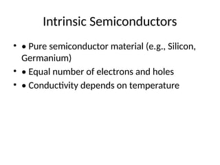
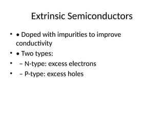
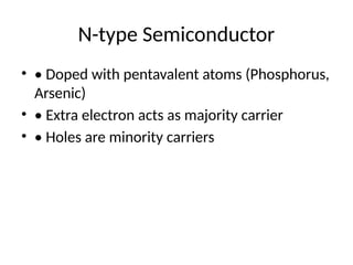
Introduction to semiconductors: Intrinsic and extrinsic
semiconductors, Energy band diagrams.
Diodes and Circuits: PN junction diode, V-I characteristics, Zener
diode, breakdown mechanism in diodes, light emitting diode.
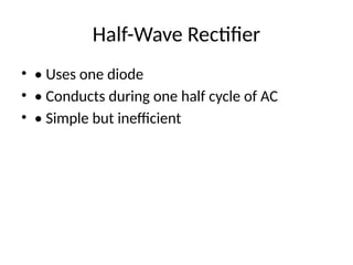
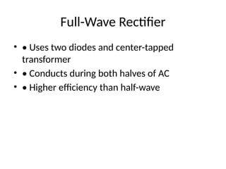
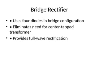
Diode Applications: Half-wave rectifier, Full-wave and Bridge
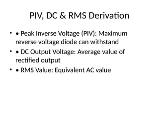
Rectifiers, PIV, derivation of DC and RMS values, Ripple Factor.
Voltage regulation using Zener diodes, C Filter, Determination of
ripple factor