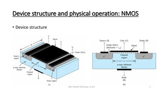
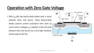
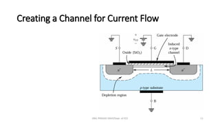
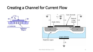
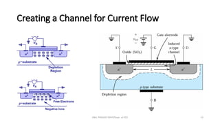
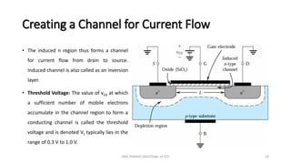
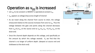
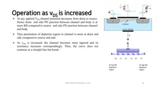
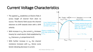
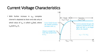
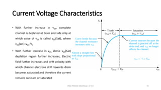
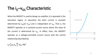
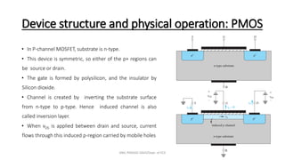
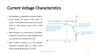
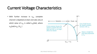
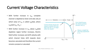
This document discusses the basics of MOSFETs, including their structure, operational principles, and characteristics such as current-voltage behavior. It covers the functionality of MOSFETs as devices used for signal amplification and as switches in electronic circuits. Key concepts include the source, drain, gate terminals, and the importance of threshold voltage in the formation of conductive channels.


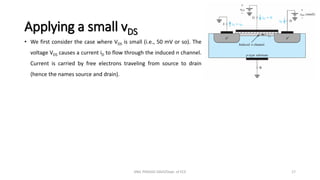
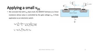
![Applying a small vDS
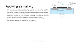
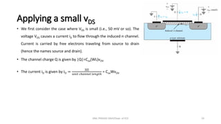
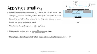
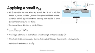
• The value of iD can now be found by multiplying the charge per unit
channel length by the electron drift velocity
iD = |Q|× vd = Cox(W)vOV × µn
𝑣𝐷𝑆
𝐿
iD = [µn Cox
𝑊
𝐿
vOV ] 𝑣𝐷𝑆
• Thus, for small vDS, the channel behaves as a linear resistance whose
value is controlled by the overdrive voltage , which in turn is
determined by vGS : iD = [µn Cox
𝑊
𝐿
(vGS-Vt) ] 𝑣𝐷𝑆
• The conductance of the channel is given by
gDS = [µn Cox
𝑊
𝐿
(vGS-Vt) ]
ANIL PRASAD DADI/Dept. of ECE 22](https://image.slidesharecdn.com/mosfetivcharacteristics-240731010022-2fc6cb74/85/MOSFET-Device-structure-Operation-with-I-V-Characteristics-pdf-22-320.jpg)


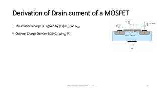
![Derivation of Drain current of a MOSFET
• The channel charge Q is given by |Q|=Cox(WL)vOV
• Channel Charge Density, |Q|=CoxW(vGS-Vt)
• Let x be a point along the channel from source to drain, and v(x)
its potential, |Q|=CoxW[vGS-v(x)-Vt]
ANIL PRASAD DADI/Dept. of ECE 32](https://image.slidesharecdn.com/mosfetivcharacteristics-240731010022-2fc6cb74/85/MOSFET-Device-structure-Operation-with-I-V-Characteristics-pdf-32-320.jpg)
![Derivation of Drain current of a MOSFET
• The channel charge Q is given by |Q|=Cox(WL)vOV
• Channel Charge Density, |Q|=CoxW(vGS-Vt)
• Let x be a point along the channel from source to drain, and v(x)
its potential, |Q|=CoxW[vGS-v(x)-Vt]
• iD = |Q|× vd = CoxW[vGS-v(x)-Vt] × µn
𝑑𝑣
𝑑𝑥
iD = µn Cox w [vGS-v(x)-Vt]
𝑑𝑣
𝑑𝑥
ANIL PRASAD DADI/Dept. of ECE 33](https://image.slidesharecdn.com/mosfetivcharacteristics-240731010022-2fc6cb74/85/MOSFET-Device-structure-Operation-with-I-V-Characteristics-pdf-33-320.jpg)
![Derivation of Drain current of a MOSFET
• iD = µn Cox w [vGS-v(x)-Vt]
𝑑𝑣
𝑑𝑥
ANIL PRASAD DADI/Dept. of ECE 34](https://image.slidesharecdn.com/mosfetivcharacteristics-240731010022-2fc6cb74/85/MOSFET-Device-structure-Operation-with-I-V-Characteristics-pdf-34-320.jpg)
![Derivation of Drain current of a MOSFET
• iD = µn Cox w [vGS-v(x)-Vt]
𝑑𝑣
𝑑𝑥
•
0
𝐿
𝑖𝐷 𝑑𝑥= µn Cox w
0
𝑣𝐷𝑆
[vGS−v(x)−Vt] dv
ANIL PRASAD DADI/Dept. of ECE 35](https://image.slidesharecdn.com/mosfetivcharacteristics-240731010022-2fc6cb74/85/MOSFET-Device-structure-Operation-with-I-V-Characteristics-pdf-35-320.jpg)
![Derivation of Drain current of a MOSFET
• iD = µn Cox w [vGS-v(x)-Vt]
𝑑𝑣
𝑑𝑥
•
0
𝐿
𝑖𝐷 𝑑𝑥= µn Cox w
0
𝑣𝐷𝑆
[vGS−v(x)−Vt] dv
• iDL= µn Cox w
0
𝑣𝐷𝑆
[vGS−Vt]dv −
0
𝑣𝐷𝑆
v(x)dv
ANIL PRASAD DADI/Dept. of ECE 36](https://image.slidesharecdn.com/mosfetivcharacteristics-240731010022-2fc6cb74/85/MOSFET-Device-structure-Operation-with-I-V-Characteristics-pdf-36-320.jpg)
![Derivation of Drain current of a MOSFET
• iD = µn Cox w [vGS-v(x)-Vt]
𝑑𝑣
𝑑𝑥
•
0
𝐿
𝑖𝐷 𝑑𝑥= µn Cox w
0
𝑣𝐷𝑆
[vGS−v(x)−Vt] dv
• iDL= µn Cox w
0
𝑣𝐷𝑆
[vGS−Vt]dv −
0
𝑣𝐷𝑆
v(x)dv
• iDL= µn Cox w| (vGS−Vt)𝑣−
𝑣2
2
|𝑣𝐷𝑆
0
ANIL PRASAD DADI/Dept. of ECE 37](https://image.slidesharecdn.com/mosfetivcharacteristics-240731010022-2fc6cb74/85/MOSFET-Device-structure-Operation-with-I-V-Characteristics-pdf-37-320.jpg)
![Derivation of Drain current of a MOSFET
• iD = µn Cox w [vGS-v(x)-Vt]
𝑑𝑣
𝑑𝑥
•
0
𝐿
𝑖𝐷 𝑑𝑥= µn Cox w
0
𝑣𝐷𝑆
[vGS−v(x)−Vt] dv
• iDL= µn Cox w
0
𝑣𝐷𝑆
[vGS−Vt]dv −
0
𝑣𝐷𝑆
v(x)dv
• iDL= µn Cox w| (vGS−Vt)𝑣−
𝑣2
2
|𝑣𝐷𝑆
0
• iDL= µn Cox w[(vGS−Vt)𝑣𝐷𝑆−
𝑣𝐷𝑆
2
2
]
ANIL PRASAD DADI/Dept. of ECE 38](https://image.slidesharecdn.com/mosfetivcharacteristics-240731010022-2fc6cb74/85/MOSFET-Device-structure-Operation-with-I-V-Characteristics-pdf-38-320.jpg)
![Derivation of Drain current of a MOSFET
• iD = µn Cox w [vGS-v(x)-Vt]
𝑑𝑣
𝑑𝑥
•
0
𝐿
𝑖𝐷 𝑑𝑥= µn Cox w
0
𝑣𝐷𝑆
[vGS−v(x)−Vt] dv
• iDL= µn Cox w
0
𝑣𝐷𝑆
[vGS−Vt]dv −
0
𝑣𝐷𝑆
v(x)dv
• iDL= µn Cox w| (vGS−Vt)𝑣−
𝑣2
2
|𝑣𝐷𝑆
0
• iDL= µn Cox w[(vGS−Vt)𝑣𝐷𝑆−
𝑣𝐷𝑆
2
2
]
• iD= µn Cox
𝑊
𝐿
[(vGS−Vt)𝑣𝐷𝑆−
𝑣𝐷𝑆
2
2
]
ANIL PRASAD DADI/Dept. of ECE 39](https://image.slidesharecdn.com/mosfetivcharacteristics-240731010022-2fc6cb74/85/MOSFET-Device-structure-Operation-with-I-V-Characteristics-pdf-39-320.jpg)
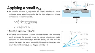
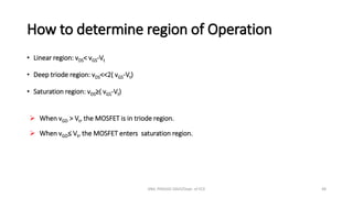
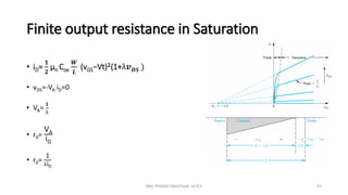
![Regions of Operation
• Linear region: vDS< vGS-Vt
iD= µn Cox
𝑾
𝑳
[(vGS−Vt)𝒗𝑫𝑺−
𝒗𝑫𝑺
𝟐
𝟐
]
• Deep triode region: vDS<<2( vGS-Vt)
iD = µn Cox
𝑾
𝑳
(vGS-Vt) 𝒗𝑫𝑺
• Saturation region: vDS≥( vGS-Vt)
iD=
𝟏
𝟐
µn Cox
𝑾
𝑳
(vGS−Vt)𝟐
ANIL PRASAD DADI/Dept. of ECE 46](https://image.slidesharecdn.com/mosfetivcharacteristics-240731010022-2fc6cb74/85/MOSFET-Device-structure-Operation-with-I-V-Characteristics-pdf-46-320.jpg)

![Regions of Operation
• Linear region: vSD< vSG-|Vtp |
iD= µp Cox
𝑾
𝑳
[(vSG−Vtp)𝒗𝑺𝑫−
𝒗𝑺𝑫
𝟐
𝟐
]
• Deep triode region: vSD<<2(vSG-|Vtp|)
iD = µp Cox
𝑾
𝑳
(vSG-Vtp) 𝒗𝑺D
• Saturation region: vSD≥(vSG-|Vtp|)
iD=
𝟏
𝟐
µpCox
𝑾
𝑳
(vSG−Vtp)𝟐
ANIL PRASAD DADI/Dept. of ECE 60](https://image.slidesharecdn.com/mosfetivcharacteristics-240731010022-2fc6cb74/85/MOSFET-Device-structure-Operation-with-I-V-Characteristics-pdf-60-320.jpg)