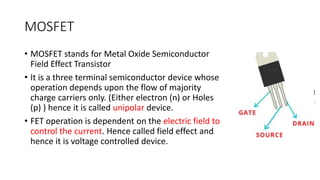
MOSFET
• MOSFET standsfor Metal Oxide Semiconductor
Field Effect Transistor
• It is a three terminal semiconductor device whose
operation depends upon the flow of majority
charge carriers only. (Either electron (n) or Holes
(p) ) hence it is called unipolar device.
• FET operation is dependent on the electric field to
control the current. Hence called field effect and
hence it is voltage controlled device.
Construction of Nchannel E MOSFET
• The basic construction of n-Channel enhancement type MOSFET is
shown in previous slide.
• A slab of P- type semiconductor material is formed from the silicion
base called substrate.
• The source and drain terminals are connected through a metallic
contacts to n –doped regions .
• The gate is also connected to a metallic contact but remains insulated
from the substrate by a thin layer of Silicon Dioxide (SiO2) Which acts
as an insulator.
• There is no channel between the two n-type materials in E MOSFET
7.
Working/ Operation ofN channel E Mosfet
• When No Gate Volltage is applied
• When Positive Gate voltage (VGS) is applied
• When small Drain to source voltage (VDS ) is applied
• When VDS is increased
8.
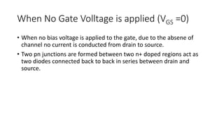
When No GateVolltage is applied (VGS =0)
• When no bias voltage is applied to the gate, due to the absene of
channel no current is conducted from drain to source.
• Two pn junctions are formed between two n+ doped regions act as
two diodes connected back to back in series between drain and
source.
9.
When Positive Gatevoltage (VGS) is applied
• When positive gate voltage is applied at the gate terminal the free holes
get repelled from under the gate. These holes are pushed downwoard into
the substrate leaving behing the depletion region.
• The positive voltage at the gate also attracts the electrons from n+ source,
and n+ drain regions and minority carriers from the substrate region into
the channel region.
• When a sufficient number of electrons accumulate under the gate, n-
channel is created connecting the source and the drain regions.
• Now current can flow through the newly formed channel if voltage is
applied between source and the drain.
• The gate voltage at which sufficient electrons accumulate to create a
channel is called Threshold Voltage (Vt)
When small Drainto source voltage (VDS ) is
applied
• Once the channel is created,
application of small VDS causes
current ID to flow through the
induced n channel.
• The value of ID depends upon the
electron density of channel
which depends on the magnitude
of VGS
12.
When VDS isincreased
• The applied voltage VDS appreas as a voltage drop across the length of the
channel.
• As we travel along the channel from source to drain the voltage increases
from 0 to VD
• Thus the voltage between the gate and point along the channel decreases
from VGS at source end to VGS -VDS at drain end.
• Since the channel depth depends on this voltage, we find that the channel
is no longer uniform in depth rather the channel will be tapered as shown
in fig 4.
• As VDS is increased further, channel becomes more tapered and its
resistance increases correspondingly. Thus the ID – VDS curve doesnot
continue as a straight line but bends as shown in characteristic curve
shown below.
Construction
• Same asE – Mosfet only change is the presence of physical channel
between drain and source.
19.
Working/ Operation ofNchannel E Mosfet
• When No Gate Volltage is applied
• When Negative Gate voltage (VGS) is applied
• When small Drain to source voltage (VDS ) is applied
• When VDS is increased
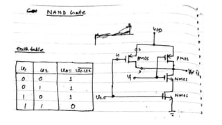
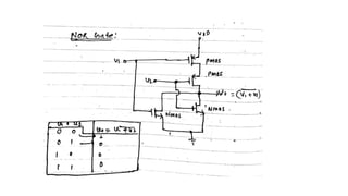
CMOS (Complementry MOSFET)
•A very effective logic circuit can be made by constructing a p-channel
and n- channel MOSFET on the same substrate as shown in figure.
• This configuration is referred to as complementary MOSFET (CMOS)
arrangement.
• It has extensive application in computer logic design.
• PMOS and NMOS are fabricated in the same substrate. N-MOS is
fabricated directly on the p-type substrate while the P-MOS is
fabricated in a specially created n region known as “n well”.