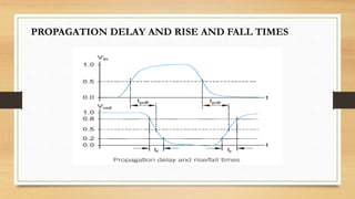
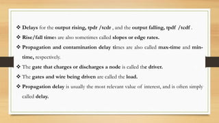
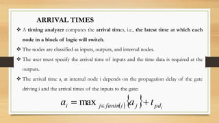
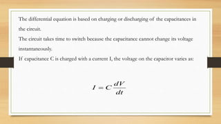
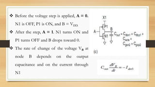
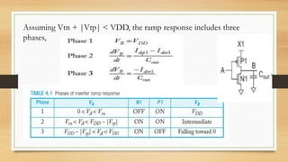
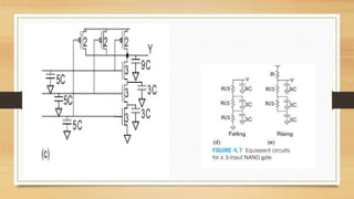
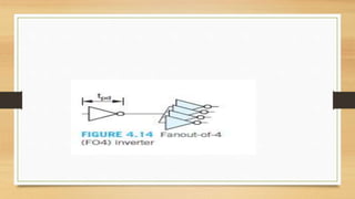
MODULE 3
DELAY
PROPAGATION DELAY AND RISE AND FALL TIMES
Propagation delay time, tpd = maximum time from the input
crossing 50% to the output crossing 50%
Contamination delay time, tcd = minimum time from the input
crossing 50% to the output crossing 50%
Rise time, tr = time for a waveform to rise from 20% to 80% of its
steady-state value
Fall time, tf = time for a waveform to fall from 80% to 20% of its
steady-state value
Edge rate, trf = (tr + tf )/2
 Delays for the output rising, tpdr /tcdr , and the output falling, tpdf /tcdf .
 Rise/fall times are also sometimes called slopes or edge rates.
 Propagation and contamination delay times are also called max-time and min-
time, respectively.
 The gate that charges or discharges a node is called the driver.
 The gates and wire being driven are called the load.
 Propagation delay is usually the most relevant value of interest, and is often simply
called delay.
 A timing analyzer computes the arrival times, i.e., the latest time at which each
node in a block of logic will switch.
 The nodes are classified as inputs, outputs, and internal nodes.
 The user must specify the arrival time of inputs and the time data is required at the
outputs.
 The arrival time ai at internal node i depends on the propagation delay of the gate
driving i and the arrival times of the inputs to the gate:
ARRIVAL TIMES
   i
pd
j
i
fanin
j
i t
a
a 
 
max
 The timing analyzer computes the arrival times at each node and
checks that the outputs arrive by their required time.
 The slack is the difference between the required and arrival
times.
 Positive slack means that the circuit meets timing.
 Negative slack means that the circuit is not fast enough.
Figure shows nodes annotated with arrival times.
If the outputs are all required at 200 ps, the circuit has 60 ps of slack.
TRANSIENT RESPONSE:
 The most fundamental way to compute delay is to develop a physical model of
the circuit of interest, write a differential equation describing the output voltage
as a function of input voltage and time, and solve the equation.
 The solution of the differential equation is called the transient response, and the
delay is the time when the output reaches VDD /2.
The differential equation is based on charging or discharging of the capacitances in
the circuit.
The circuit takes time to switch because the capacitance cannot change its voltage
instantaneously.
If capacitance C is charged with a current I, the voltage on the capacitor varies as:
dt
dV
C
I 
MOSFET Capacitance
-the Capacitances of a MOSFET are considered parasitic
-"parasitic" means unwanted or unintentional.
They are unavoidable and a result of fabricating the devices using
physical materials.
-we can use the capacitances of the MOSFET to estimate factors such as
rise time, delay, fan-out, and propagation delay
MOSFET Capacitance
-Capacitance = Charge / Volt = (C/V)
MOSFET Capacitance
-We group the various capacitances into two groups
1) Oxide Capacitances-capacitance due to the Gate oxide
2) Junction Capacitances -capacitance due to the Source/Drain
diffusion regions
Capacitances for inverter delay calculations
 Figure (a) shows an inverter X1 driving another inverter X2 at the end of a wire.
 Suppose a voltage step from 0 to VDD is applied to node A and we wish to
compute the propagation delay, tpdf , through X1, i.e., the delay from the input
step until node B crosses VDD/2.
TRANSIENT RESPONSE: contd........
Figure (c) shows the equivalent circuit diagram in which all the
capacitances are lumped into a single Cout.
 Before the voltage step is applied, A = 0.
N1 is OFF, P1 is ON, and B = VDD.
 After the step, A = 1. N1 turns ON and
P1 turns OFF and B drops toward 0.
 The rate of change of the voltage VB at
node B depends on the output
capacitance and on the current through
N1
 The current depends on whether N1 is in the linear or saturation
regime.
 The gate is at VDD, the source is at 0, and the drain is at VB.
 Thus, Vgs = VDD and Vds = VB. Initially, Vds = VDD > Vgs – Vt , so
N1 is in saturation. As VB falls below VDD – Vt , N1 enters the linear
regime.
Assuming Vtn + |Vtp| < VDD, the ramp response includes three
phases,
 The key observation is that the propagation delay increases because
N1 is not fully ON right away and because it must fight P1 in Phase 2.
 More complex gates such as NANDs or NORs have transistors in
series.
 If the transistors have the same dimensions and the load is the same,
the delay will increase with the number of series transistors.
 The physical modeling shows that the delay increases with the output
capacitance and decreases with the driver current.
 The differential equations used the long-channel model for transistor
current, which is inaccurate in modern processes.
 The equations are also too nonlinear to solve in closed form, so they
have to be solved numerically and give little insight about delay.
RC Delay Model
- approximates the nonlinear transistor I-V and C-V characteristics
- with an average resistance and capacitance
- over the switching range of the gate.
Effective Resistance
The RC delay model treats a transistor as a switch in series with a resistor.
The effective resistance is the ratio of Vds to Ids averaged across the switching
interval of interest.
According to the long-channel model, current decreases linearly with channel
length and hence resistance is proportional to L.
The resistance of two transistors in series is the sum of the resistances of each
transistor
An nMOS ransistor of k times unit width has resistance R/k because it
delivers k times as much current.
A unit pMOS transistor has greater resistance, generally in the range of 2R–
3R,
because of its lower mobility.
Gate and Diffusion Capacitance
Each transistor also has gate and diffusion capacitance.
We define C to be the gate capacitance of a unit transistor.
A transistor of k times unit width has capacitance kC.
Diffusion capacitance depends on the size of the source/drain region
Increasing channel length increases gate capacitance proportionally but does
not affect diffusion capacitance.
The unit inverters of Figure 4.6(a) are composed from an nMOS transistor of unit size
and a pMOS transistor of twice unit width to achieve equal rise and fall resistance.
Example 4.2
Sketch a 3-input NAND gate with transistor widths chosen to achieve effective rise
and fall resistance equal to that of a unit inverter (R). Annotate the gate with its gate
and diffusion capacitances. Assume all diffusion nodes are contacted. Then sketch
equivalent circuits for the falling output transition and for the worst-case rising
output transition.
The RC model to estimate the step response of the first-order
system shown in Figure 4.8.
The system has a transfer function and a step response
where τ= RC. The propagation delay is the time at which Vout reaches VDD/2
R’ = R ln 2.
The RC model to estimate the step response of the second-order system
shown in Figure 4.10.
R1 and R2 might model the two series nMOS transistors in a NAND gate or
an inverter driving a long wire with non-negligible resistance.
The transfer function is
EQ (4.12) is so complicated that it defeats the purpose of
simplifying a CMOS circuit into an equivalent RC network.
However, it can be further approximated as a first order system
with a single time constant:
This approximation works best when one time constant is significantly
bigger than the other.
For example, if R1 = R2 = R and C1 = C2 = C, then τ1 = 2.6 RC,τ2 =
0.4 RC, τ= 3 RC and the second-order response and its first-order
approximation are shown in Figure 4.11.
The error in estimated propagation delay from the first-order
approximation is less than 7%.
Even in the worst case, where the two time constants are equal, the
error is less than 15%.
 Most circuits of interest can be represented as an RC tree, i.e., an RC circuit with
no loops.
 The root of the tree is the voltage source and the leaves are the capacitors at the
ends of the branches.
 The Elmore delay model estimates the delay from a source switching to one of
the leaf nodes changing as the sum over each node i of the capacitance Ci on the
node, multiplied by the effective resistance Ris on the shared path from the source
to the node and the leaf.
Elmore Delay
Example 4.3
Compute the Elmore delay for Vout in the 2nd order RC system.
SOLUTION: The circuit has a source and two nodes. At node n1, the capacitance
is C1 and the resistance to the source is R1.
At node Vout, the capacitance is C2 and the resistance to the source is (R1 + R2).
Hence, the Elmore delay is tpd = R1C1 + (R1 + R2)C2
Note that the effective resistances should account for the factor of ln 2.
Example 4.4
Estimate tpd for a unit inverter driving m identical unit inverters.
SOLUTION: Figure 4.12 shows an equivalent circuit for the falling transition.
Each load inverter presents 3C units of gate capacitance, for a total of 3mC.
The output node also sees a capacitance of 3C from the drain diffusions of the
driving inverter.
This capacitance is called parasitic because it is an undesired side-effect of the need to
make the drain large enough to contact.
The parasitic capacitance is independent of the load that the inverter is driving. Hence,
the total capacitance is (3 + 3m)C. The resistance is R, so the Elmore delay is tpd = (3
+ 3m)RC.
The equivalent circuit for the rising transition gives the same results.
Example 4.5
Repeat Example 4.4 if the driver is w times unit size.
SOLUTION: Figure 4.13 shows the equivalent circuit.
The driver transistors are w times as wide, so the effective resistance decreases by a
factor of w .
The diffusion capacitance increases by a factor of w.
The Elmore delay is tpd = ((3w + 3m)C)(R/w) = (3 + 3m/w)RC.
Define the fanout of the gate, h, to be the ratio of the load capacitance to the input
capacitance. (Diffusion capacitance is not counted in the fanout.) The load
capacitance
is 3mC. The input capacitance is 3wC. Thus, the inverter has a fanout of h = m/w
and
the delay can be written as (3 + 3h)RC.
Example 4.6
If a unit transistor has R = 10 kΩand C = 0.1 fF in a 65 nm process, compute
the delay, in picoseconds, of the inverter in Figure 4.14 with a fanout of h = 4.
SOLUTION: The RC product in the 65 nm process is (10 kΩ)(0.1 fF) = 1 ps.
For h = 4, the delay is (3 + 3h)(1 ps) = 15 ps. This is called the fanout-of-4 (FO4)
inverter delay and is representative of gate delays in a typical circuit.
The inverter can switch about 66 billion times per second (1/15ps). This
stunning speed partially explains the fantastic capabilities of integrated circuits.
VLSIM3.pptx

VLSIM3.pptx

  • 1.
  • 2.
    PROPAGATION DELAY ANDRISE AND FALL TIMES
  • 3.
    Propagation delay time,tpd = maximum time from the input crossing 50% to the output crossing 50% Contamination delay time, tcd = minimum time from the input crossing 50% to the output crossing 50% Rise time, tr = time for a waveform to rise from 20% to 80% of its steady-state value Fall time, tf = time for a waveform to fall from 80% to 20% of its steady-state value Edge rate, trf = (tr + tf )/2
  • 4.
     Delays forthe output rising, tpdr /tcdr , and the output falling, tpdf /tcdf .  Rise/fall times are also sometimes called slopes or edge rates.  Propagation and contamination delay times are also called max-time and min- time, respectively.  The gate that charges or discharges a node is called the driver.  The gates and wire being driven are called the load.  Propagation delay is usually the most relevant value of interest, and is often simply called delay.
  • 5.
     A timinganalyzer computes the arrival times, i.e., the latest time at which each node in a block of logic will switch.  The nodes are classified as inputs, outputs, and internal nodes.  The user must specify the arrival time of inputs and the time data is required at the outputs.  The arrival time ai at internal node i depends on the propagation delay of the gate driving i and the arrival times of the inputs to the gate: ARRIVAL TIMES    i pd j i fanin j i t a a    max
  • 6.
     The timinganalyzer computes the arrival times at each node and checks that the outputs arrive by their required time.  The slack is the difference between the required and arrival times.  Positive slack means that the circuit meets timing.  Negative slack means that the circuit is not fast enough.
  • 7.
    Figure shows nodesannotated with arrival times. If the outputs are all required at 200 ps, the circuit has 60 ps of slack.
  • 8.
    TRANSIENT RESPONSE:  Themost fundamental way to compute delay is to develop a physical model of the circuit of interest, write a differential equation describing the output voltage as a function of input voltage and time, and solve the equation.  The solution of the differential equation is called the transient response, and the delay is the time when the output reaches VDD /2.
  • 9.
    The differential equationis based on charging or discharging of the capacitances in the circuit. The circuit takes time to switch because the capacitance cannot change its voltage instantaneously. If capacitance C is charged with a current I, the voltage on the capacitor varies as: dt dV C I 
  • 10.
    MOSFET Capacitance -the Capacitancesof a MOSFET are considered parasitic -"parasitic" means unwanted or unintentional. They are unavoidable and a result of fabricating the devices using physical materials. -we can use the capacitances of the MOSFET to estimate factors such as rise time, delay, fan-out, and propagation delay
  • 11.
    MOSFET Capacitance -Capacitance =Charge / Volt = (C/V)
  • 12.
    MOSFET Capacitance -We groupthe various capacitances into two groups 1) Oxide Capacitances-capacitance due to the Gate oxide 2) Junction Capacitances -capacitance due to the Source/Drain diffusion regions
  • 13.
    Capacitances for inverterdelay calculations  Figure (a) shows an inverter X1 driving another inverter X2 at the end of a wire.  Suppose a voltage step from 0 to VDD is applied to node A and we wish to compute the propagation delay, tpdf , through X1, i.e., the delay from the input step until node B crosses VDD/2.
  • 14.
    TRANSIENT RESPONSE: contd........ Figure(c) shows the equivalent circuit diagram in which all the capacitances are lumped into a single Cout.
  • 15.
     Before thevoltage step is applied, A = 0. N1 is OFF, P1 is ON, and B = VDD.  After the step, A = 1. N1 turns ON and P1 turns OFF and B drops toward 0.  The rate of change of the voltage VB at node B depends on the output capacitance and on the current through N1
  • 16.
     The currentdepends on whether N1 is in the linear or saturation regime.  The gate is at VDD, the source is at 0, and the drain is at VB.  Thus, Vgs = VDD and Vds = VB. Initially, Vds = VDD > Vgs – Vt , so N1 is in saturation. As VB falls below VDD – Vt , N1 enters the linear regime.
  • 17.
    Assuming Vtn +|Vtp| < VDD, the ramp response includes three phases,
  • 18.
     The keyobservation is that the propagation delay increases because N1 is not fully ON right away and because it must fight P1 in Phase 2.  More complex gates such as NANDs or NORs have transistors in series.  If the transistors have the same dimensions and the load is the same, the delay will increase with the number of series transistors.  The physical modeling shows that the delay increases with the output capacitance and decreases with the driver current.
  • 19.
     The differentialequations used the long-channel model for transistor current, which is inaccurate in modern processes.  The equations are also too nonlinear to solve in closed form, so they have to be solved numerically and give little insight about delay.
  • 20.
    RC Delay Model -approximates the nonlinear transistor I-V and C-V characteristics - with an average resistance and capacitance - over the switching range of the gate.
  • 21.
    Effective Resistance The RCdelay model treats a transistor as a switch in series with a resistor. The effective resistance is the ratio of Vds to Ids averaged across the switching interval of interest. According to the long-channel model, current decreases linearly with channel length and hence resistance is proportional to L. The resistance of two transistors in series is the sum of the resistances of each transistor
  • 22.
    An nMOS ransistorof k times unit width has resistance R/k because it delivers k times as much current. A unit pMOS transistor has greater resistance, generally in the range of 2R– 3R, because of its lower mobility.
  • 23.
    Gate and DiffusionCapacitance Each transistor also has gate and diffusion capacitance. We define C to be the gate capacitance of a unit transistor. A transistor of k times unit width has capacitance kC. Diffusion capacitance depends on the size of the source/drain region Increasing channel length increases gate capacitance proportionally but does not affect diffusion capacitance.
  • 25.
    The unit invertersof Figure 4.6(a) are composed from an nMOS transistor of unit size and a pMOS transistor of twice unit width to achieve equal rise and fall resistance.
  • 26.
    Example 4.2 Sketch a3-input NAND gate with transistor widths chosen to achieve effective rise and fall resistance equal to that of a unit inverter (R). Annotate the gate with its gate and diffusion capacitances. Assume all diffusion nodes are contacted. Then sketch equivalent circuits for the falling output transition and for the worst-case rising output transition.
  • 29.
    The RC modelto estimate the step response of the first-order system shown in Figure 4.8. The system has a transfer function and a step response
  • 30.
    where τ= RC.The propagation delay is the time at which Vout reaches VDD/2 R’ = R ln 2.
  • 31.
    The RC modelto estimate the step response of the second-order system shown in Figure 4.10. R1 and R2 might model the two series nMOS transistors in a NAND gate or an inverter driving a long wire with non-negligible resistance.
  • 32.
  • 33.
    EQ (4.12) isso complicated that it defeats the purpose of simplifying a CMOS circuit into an equivalent RC network. However, it can be further approximated as a first order system with a single time constant:
  • 34.
    This approximation worksbest when one time constant is significantly bigger than the other. For example, if R1 = R2 = R and C1 = C2 = C, then τ1 = 2.6 RC,τ2 = 0.4 RC, τ= 3 RC and the second-order response and its first-order approximation are shown in Figure 4.11.
  • 35.
    The error inestimated propagation delay from the first-order approximation is less than 7%. Even in the worst case, where the two time constants are equal, the error is less than 15%.
  • 36.
     Most circuitsof interest can be represented as an RC tree, i.e., an RC circuit with no loops.  The root of the tree is the voltage source and the leaves are the capacitors at the ends of the branches.  The Elmore delay model estimates the delay from a source switching to one of the leaf nodes changing as the sum over each node i of the capacitance Ci on the node, multiplied by the effective resistance Ris on the shared path from the source to the node and the leaf. Elmore Delay
  • 37.
    Example 4.3 Compute theElmore delay for Vout in the 2nd order RC system. SOLUTION: The circuit has a source and two nodes. At node n1, the capacitance is C1 and the resistance to the source is R1. At node Vout, the capacitance is C2 and the resistance to the source is (R1 + R2). Hence, the Elmore delay is tpd = R1C1 + (R1 + R2)C2 Note that the effective resistances should account for the factor of ln 2.
  • 38.
    Example 4.4 Estimate tpdfor a unit inverter driving m identical unit inverters. SOLUTION: Figure 4.12 shows an equivalent circuit for the falling transition. Each load inverter presents 3C units of gate capacitance, for a total of 3mC. The output node also sees a capacitance of 3C from the drain diffusions of the driving inverter. This capacitance is called parasitic because it is an undesired side-effect of the need to make the drain large enough to contact. The parasitic capacitance is independent of the load that the inverter is driving. Hence, the total capacitance is (3 + 3m)C. The resistance is R, so the Elmore delay is tpd = (3 + 3m)RC. The equivalent circuit for the rising transition gives the same results.
  • 40.
    Example 4.5 Repeat Example4.4 if the driver is w times unit size. SOLUTION: Figure 4.13 shows the equivalent circuit. The driver transistors are w times as wide, so the effective resistance decreases by a factor of w . The diffusion capacitance increases by a factor of w. The Elmore delay is tpd = ((3w + 3m)C)(R/w) = (3 + 3m/w)RC. Define the fanout of the gate, h, to be the ratio of the load capacitance to the input capacitance. (Diffusion capacitance is not counted in the fanout.) The load capacitance is 3mC. The input capacitance is 3wC. Thus, the inverter has a fanout of h = m/w and the delay can be written as (3 + 3h)RC.
  • 42.
    Example 4.6 If aunit transistor has R = 10 kΩand C = 0.1 fF in a 65 nm process, compute the delay, in picoseconds, of the inverter in Figure 4.14 with a fanout of h = 4. SOLUTION: The RC product in the 65 nm process is (10 kΩ)(0.1 fF) = 1 ps. For h = 4, the delay is (3 + 3h)(1 ps) = 15 ps. This is called the fanout-of-4 (FO4) inverter delay and is representative of gate delays in a typical circuit. The inverter can switch about 66 billion times per second (1/15ps). This stunning speed partially explains the fantastic capabilities of integrated circuits.