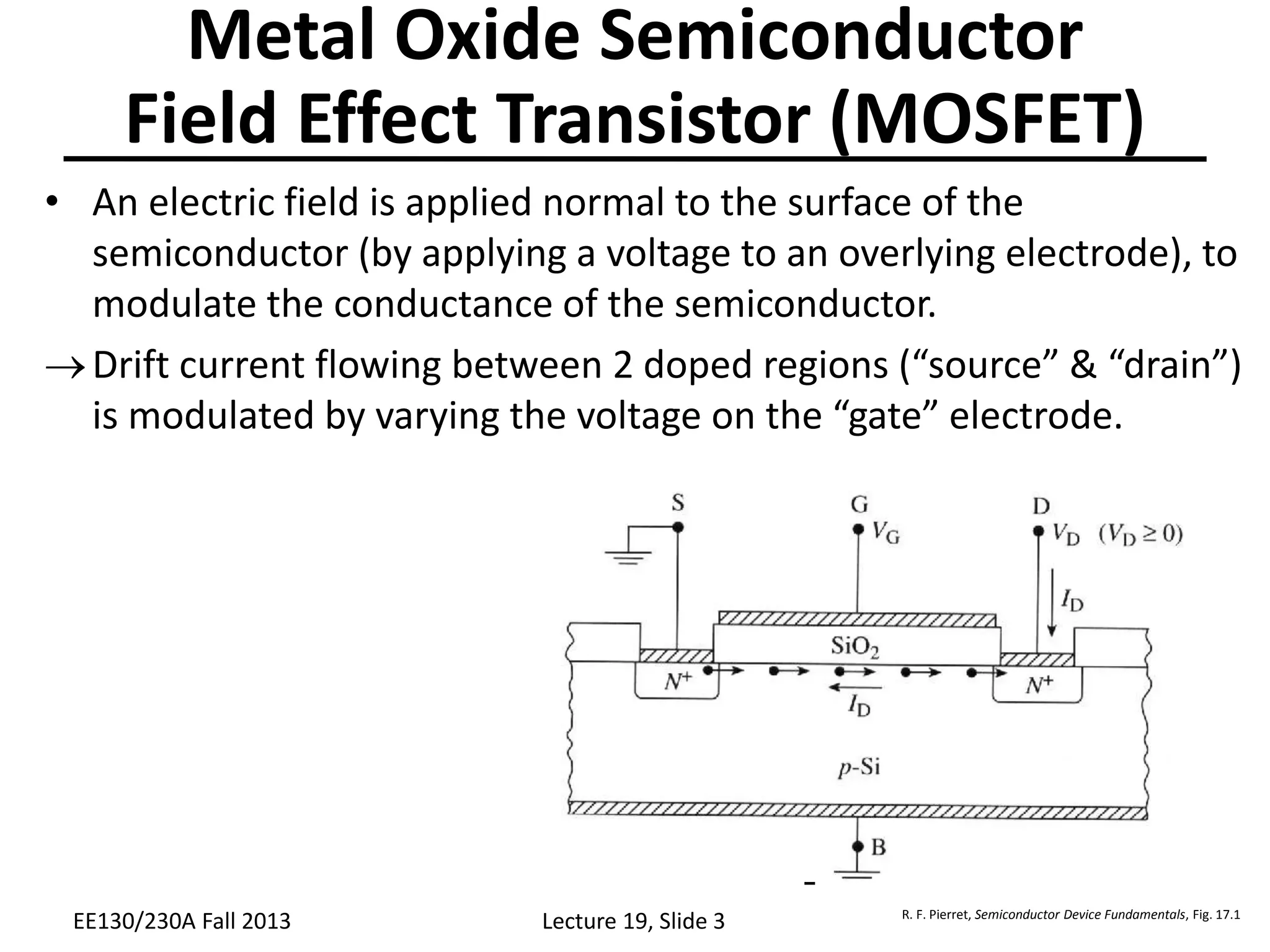
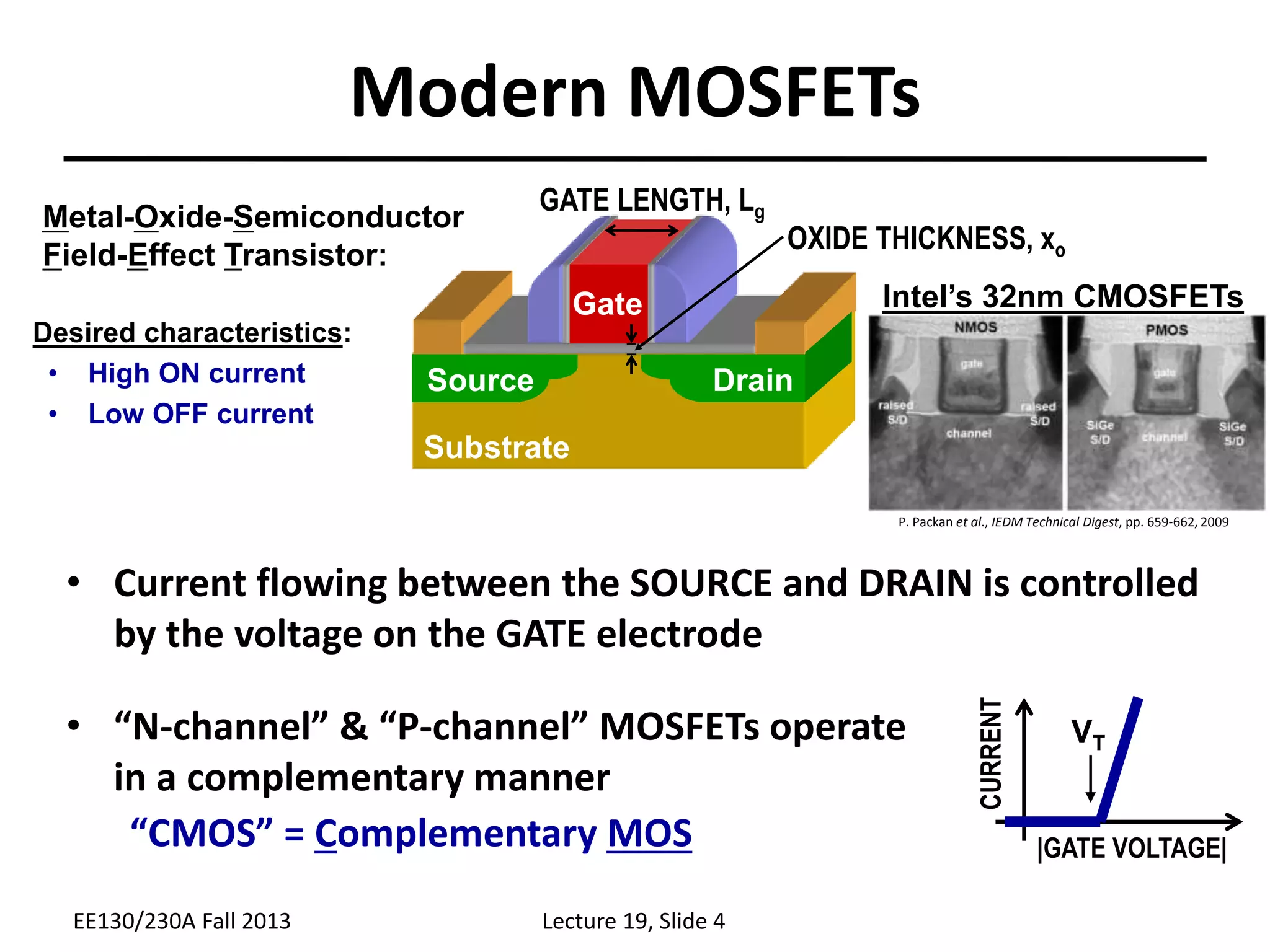
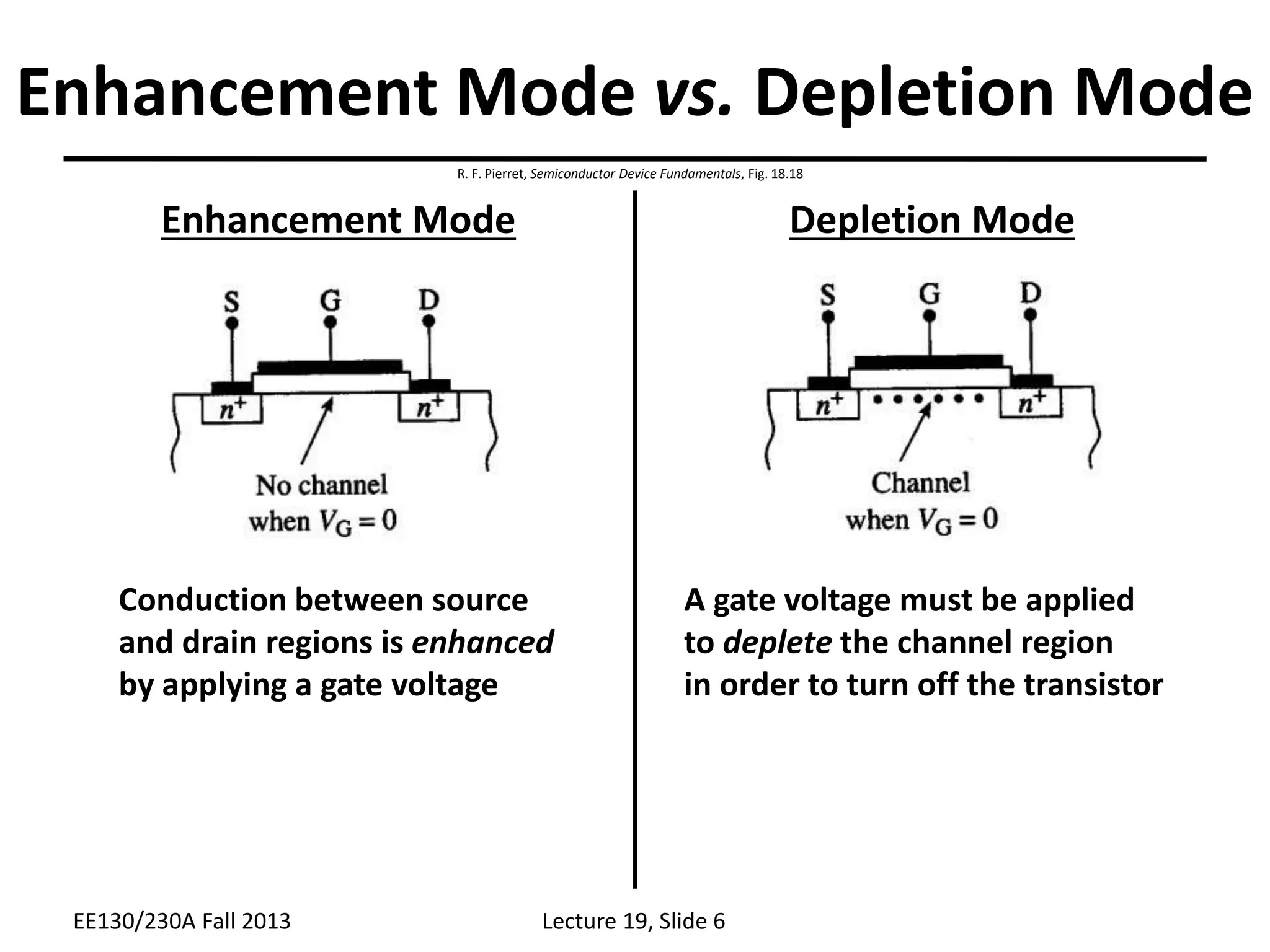
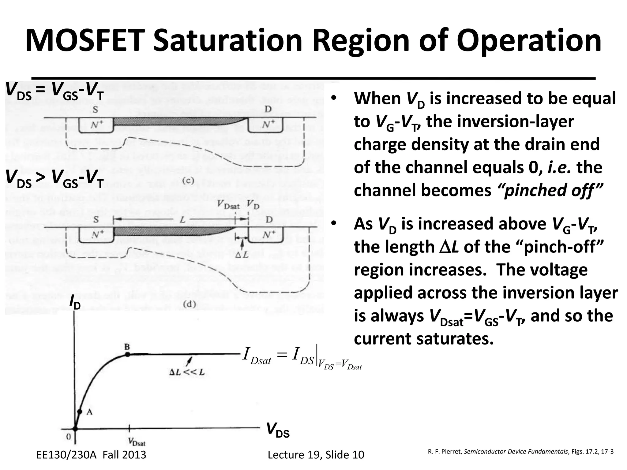
OUTLINE
The MOSFET:
• Structure and operation
• Qualitative theory of operation
• Field-effect mobility
• Body bias effect
MOSFET Devices
In 1935, a British patent was issued to Oskar Heil.
A working MOSFET was not demonstrated until 1955.
Invention of the Field-Effect Transistor
Lecture 19, Slide 2
EE130/230A Fall 2013
O. Heil, British Patent 439,457 (1935)
Metal Oxide Semiconductor
Field Effect Transistor (MOSFET)
• An electric field is applied normal to the surface of the
semiconductor (by applying a voltage to an overlying electrode), to
modulate the conductance of the semiconductor.
Drift current flowing between 2 doped regions (“source” & “drain”)
is modulated by varying the voltage on the “gate” electrode.
Lecture 19, Slide 3
EE130/230A Fall 2013 R. F. Pierret, Semiconductor Device Fundamentals, Fig. 17.1
Modern MOSFETs
4
• Current flowing between the SOURCE and DRAIN is controlled
by the voltage on the GATE electrode
Substrate
Gate
Source Drain
Metal-Oxide-Semiconductor
Field-Effect Transistor:
GATE LENGTH, Lg
OXIDE THICKNESS, xo
Desired characteristics:
• High ON current
• Low OFF current
• “N-channel” & “P-channel” MOSFETs operate
in a complementary manner
“CMOS” = Complementary MOS |GATE VOLTAGE|
CURRENT
VT
Intel’s 32nm CMOSFETs
Lecture 19, Slide 4
EE130/230A Fall 2013
P. Packan et al., IEDM Technical Digest, pp. 659-662, 2009
N-channel vs. P-channel
• For current to flow, VGS > VT
to form n-type channel at surface
• Enhancement mode: VT > 0
• Depletion mode: VT < 0
Transistor is ON when VG=0V
p-type Si
N+ poly-Si
n-type Si
P+ poly-Si
NMOS PMOS
N+ N+ P+ P+
• For current to flow, VGS < VT
to form p-type channel at surface
• Enhancement mode: VT < 0
• Depletion mode: VT > 0
Transistor is ON when VG=0V
Lecture 19, Slide 5
EE130/230A Fall 2013
Enhancement Mode vs. Depletion Mode
Enhancement Mode Depletion Mode
Conduction between source
and drain regions is enhanced
by applying a gate voltage
A gate voltage must be applied
to deplete the channel region
in order to turn off the transistor
Lecture 19, Slide 6
EE130/230A Fall 2013
R. F. Pierret, Semiconductor Device Fundamentals, Fig. 18.18
CMOS Devices and Circuits
CIRCUIT SYMBOLS
N-channel
MOSFET
P-channel
MOSFET
GND
VDD
S
S
D
D
CMOS INVERTER CIRCUIT
VIN VOUT
VOUT
VIN
0 VDD
VDD
INVERTER
LOGIC SYMBOL
• When VG = VDD , the NMOSFET is on and the PMOSFET is off.
• When VG = 0, the PMOSFET is on and the NMOSFET is off.
Lecture 19, Slide 7
EE130/230A Fall 2013
“Pull-Down” and “Pull-Up” Devices
• In CMOS logic gates, NMOSFETs are used to connect
the output to GND, whereas PMOSFETs are used to
connect the output to VDD.
– An NMOSFET functions as a pull-down device when it is
turned on (gate voltage = VDD)
– A PMOSFET functions as a pull-up device when it is turned
on (gate voltage = GND)
F(A1, A2, …, AN)
PMOSFETs only
NMOSFETs only
Pull-up
network
Pull-down
network
VDD
A1
A2
AN
A1
A2
AN
input signals
Lecture 19, Slide 8
EE130/230A Fall 2013
Qualitative Theory of the NMOSFET
depletion layer
The potential barrier to electron flow from the source
into the channel region is lowered by applying VGS> VT
Electrons flow from the
source to the drain by drift,
when VDS>0. (IDS > 0)
The channel potential
varies from VS at the source
end to VD at the drain end.
VGS < VT :
VGS > VT :
VDS  0
VDS > 0
Inversion-layer
“channel” is formed
EE130/230A Fall 2013 Lecture 19, Slide 9 R. F. Pierret, Semiconductor Device Fundamentals, Fig. 17.2
• When VD is increased to be equal
to VG-VT, the inversion-layer
charge density at the drain end
of the channel equals 0, i.e. the
channel becomes “pinched off”
• As VD is increased above VG-VT,
the length DL of the “pinch-off”
region increases. The voltage
applied across the inversion layer
is always VDsat=VGS-VT, and so the
current saturates.
VDS = VGS-VT
VDS > VGS-VT
VDS
MOSFET Saturation Region of Operation
Dsat
DS V
V
DS
Dsat I
I 

ID
EE130/230A Fall 2013 Lecture 19, Slide 10 R. F. Pierret, Semiconductor Device Fundamentals, Figs. 17.2, 17-3
Ideal NMOSFET I-V Characteristics
EE130/230A Fall 2013 Lecture 19, Slide 11 R. F. Pierret, Semiconductor Device Fundamentals, Fig. 17.4
Channel Length Modulation
• As VDS is increased above VDsat, the width DL of the depletion
region between the pinch-off point and the drain increases,
i.e. the inversion layer length decreases.





 D


D


L
L
L
L
L
IDsat 1
1
1
Dsat
DS V
V
L 

D
 
Dsat
DS V
V
L
L


D

 
 
Dsat
DS
Dsat
Dsat V
V
I
I 

 
1
0
IDS
VDS
If DL is significant compared to L,
then IDS will increase slightly with
increasing VDS>VDsat, due to
“channel-length modulation”
EE130/230A Fall 2013 Lecture 19, Slide 12 R. F. Pierret, Semiconductor Device Fundamentals, Figs. 17.2, 17-3

MOSFET devices.ppt

  • 1.
    OUTLINE The MOSFET: • Structureand operation • Qualitative theory of operation • Field-effect mobility • Body bias effect MOSFET Devices
  • 2.
    In 1935, aBritish patent was issued to Oskar Heil. A working MOSFET was not demonstrated until 1955. Invention of the Field-Effect Transistor Lecture 19, Slide 2 EE130/230A Fall 2013 O. Heil, British Patent 439,457 (1935)
  • 3.
    Metal Oxide Semiconductor FieldEffect Transistor (MOSFET) • An electric field is applied normal to the surface of the semiconductor (by applying a voltage to an overlying electrode), to modulate the conductance of the semiconductor. Drift current flowing between 2 doped regions (“source” & “drain”) is modulated by varying the voltage on the “gate” electrode. Lecture 19, Slide 3 EE130/230A Fall 2013 R. F. Pierret, Semiconductor Device Fundamentals, Fig. 17.1
  • 4.
    Modern MOSFETs 4 • Currentflowing between the SOURCE and DRAIN is controlled by the voltage on the GATE electrode Substrate Gate Source Drain Metal-Oxide-Semiconductor Field-Effect Transistor: GATE LENGTH, Lg OXIDE THICKNESS, xo Desired characteristics: • High ON current • Low OFF current • “N-channel” & “P-channel” MOSFETs operate in a complementary manner “CMOS” = Complementary MOS |GATE VOLTAGE| CURRENT VT Intel’s 32nm CMOSFETs Lecture 19, Slide 4 EE130/230A Fall 2013 P. Packan et al., IEDM Technical Digest, pp. 659-662, 2009
  • 5.
    N-channel vs. P-channel •For current to flow, VGS > VT to form n-type channel at surface • Enhancement mode: VT > 0 • Depletion mode: VT < 0 Transistor is ON when VG=0V p-type Si N+ poly-Si n-type Si P+ poly-Si NMOS PMOS N+ N+ P+ P+ • For current to flow, VGS < VT to form p-type channel at surface • Enhancement mode: VT < 0 • Depletion mode: VT > 0 Transistor is ON when VG=0V Lecture 19, Slide 5 EE130/230A Fall 2013
  • 6.
    Enhancement Mode vs.Depletion Mode Enhancement Mode Depletion Mode Conduction between source and drain regions is enhanced by applying a gate voltage A gate voltage must be applied to deplete the channel region in order to turn off the transistor Lecture 19, Slide 6 EE130/230A Fall 2013 R. F. Pierret, Semiconductor Device Fundamentals, Fig. 18.18
  • 7.
    CMOS Devices andCircuits CIRCUIT SYMBOLS N-channel MOSFET P-channel MOSFET GND VDD S S D D CMOS INVERTER CIRCUIT VIN VOUT VOUT VIN 0 VDD VDD INVERTER LOGIC SYMBOL • When VG = VDD , the NMOSFET is on and the PMOSFET is off. • When VG = 0, the PMOSFET is on and the NMOSFET is off. Lecture 19, Slide 7 EE130/230A Fall 2013
  • 8.
    “Pull-Down” and “Pull-Up”Devices • In CMOS logic gates, NMOSFETs are used to connect the output to GND, whereas PMOSFETs are used to connect the output to VDD. – An NMOSFET functions as a pull-down device when it is turned on (gate voltage = VDD) – A PMOSFET functions as a pull-up device when it is turned on (gate voltage = GND) F(A1, A2, …, AN) PMOSFETs only NMOSFETs only Pull-up network Pull-down network VDD A1 A2 AN A1 A2 AN input signals Lecture 19, Slide 8 EE130/230A Fall 2013
  • 9.
    Qualitative Theory ofthe NMOSFET depletion layer The potential barrier to electron flow from the source into the channel region is lowered by applying VGS> VT Electrons flow from the source to the drain by drift, when VDS>0. (IDS > 0) The channel potential varies from VS at the source end to VD at the drain end. VGS < VT : VGS > VT : VDS  0 VDS > 0 Inversion-layer “channel” is formed EE130/230A Fall 2013 Lecture 19, Slide 9 R. F. Pierret, Semiconductor Device Fundamentals, Fig. 17.2
  • 10.
    • When VDis increased to be equal to VG-VT, the inversion-layer charge density at the drain end of the channel equals 0, i.e. the channel becomes “pinched off” • As VD is increased above VG-VT, the length DL of the “pinch-off” region increases. The voltage applied across the inversion layer is always VDsat=VGS-VT, and so the current saturates. VDS = VGS-VT VDS > VGS-VT VDS MOSFET Saturation Region of Operation Dsat DS V V DS Dsat I I   ID EE130/230A Fall 2013 Lecture 19, Slide 10 R. F. Pierret, Semiconductor Device Fundamentals, Figs. 17.2, 17-3
  • 11.
    Ideal NMOSFET I-VCharacteristics EE130/230A Fall 2013 Lecture 19, Slide 11 R. F. Pierret, Semiconductor Device Fundamentals, Fig. 17.4
  • 12.
    Channel Length Modulation •As VDS is increased above VDsat, the width DL of the depletion region between the pinch-off point and the drain increases, i.e. the inversion layer length decreases.       D   D   L L L L L IDsat 1 1 1 Dsat DS V V L   D   Dsat DS V V L L   D      Dsat DS Dsat Dsat V V I I     1 0 IDS VDS If DL is significant compared to L, then IDS will increase slightly with increasing VDS>VDsat, due to “channel-length modulation” EE130/230A Fall 2013 Lecture 19, Slide 12 R. F. Pierret, Semiconductor Device Fundamentals, Figs. 17.2, 17-3