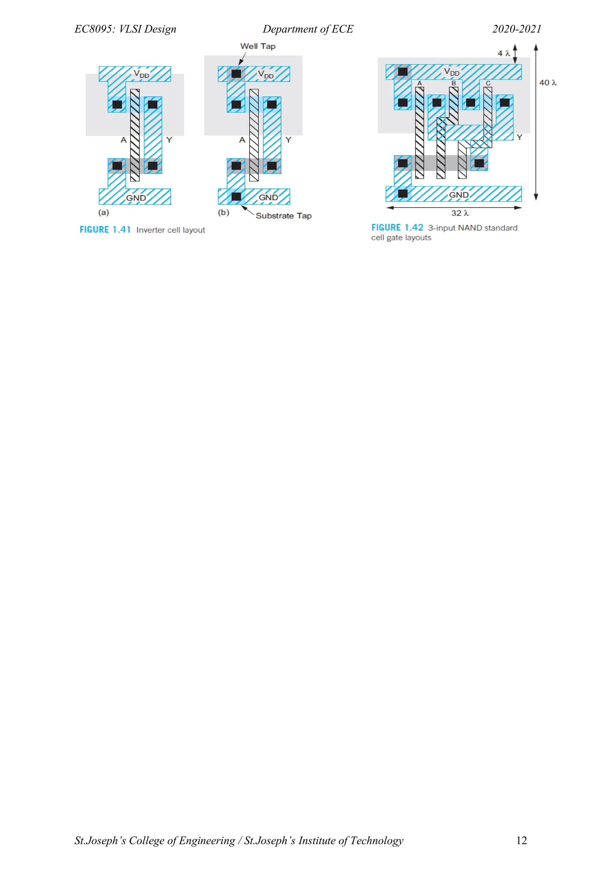
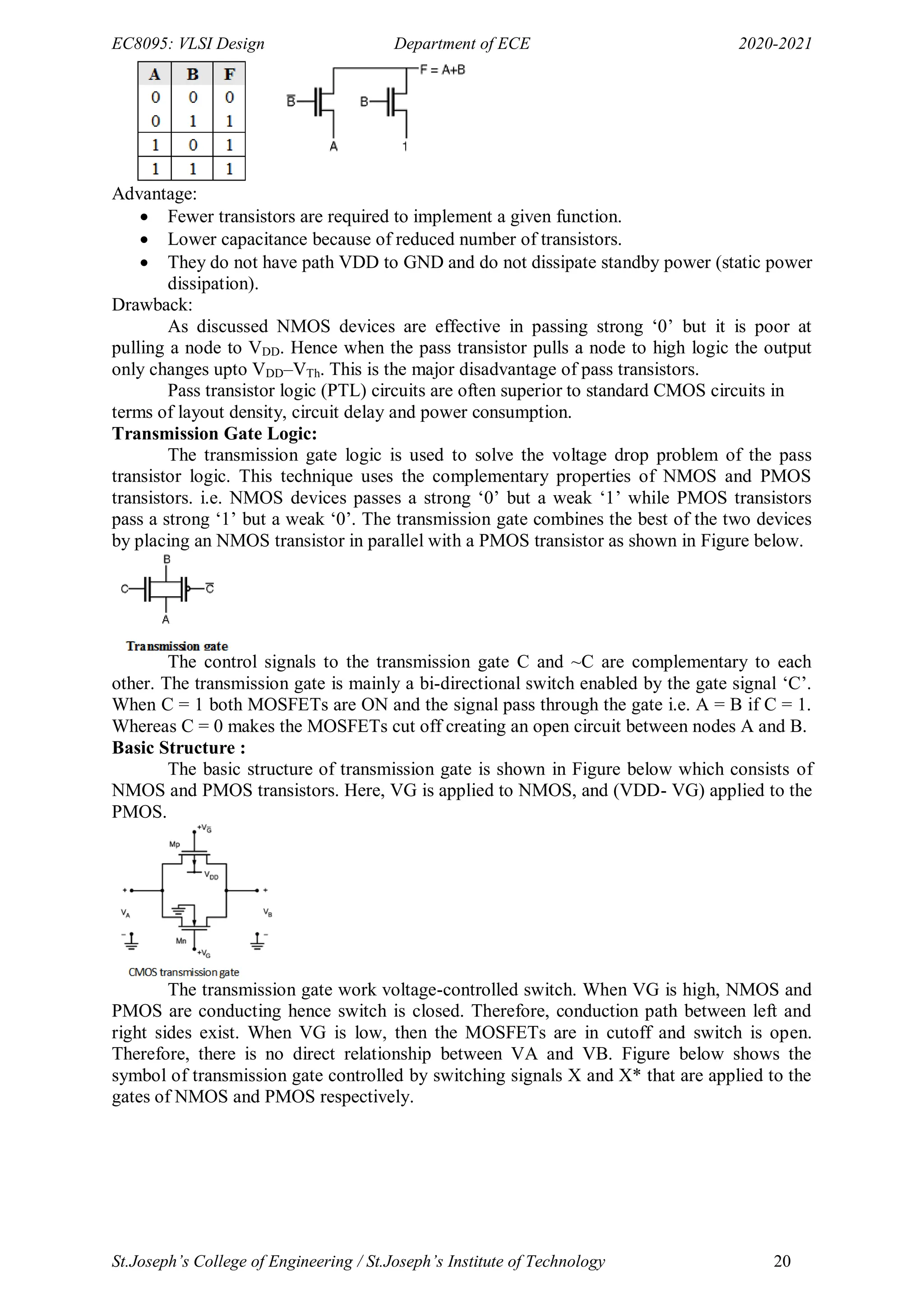
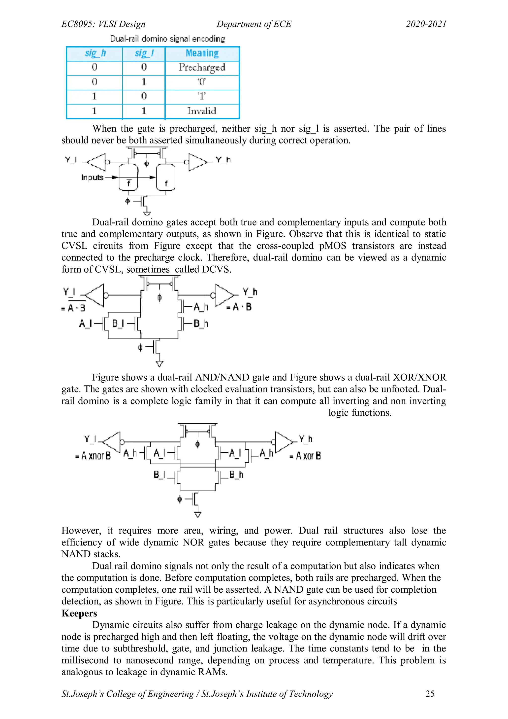
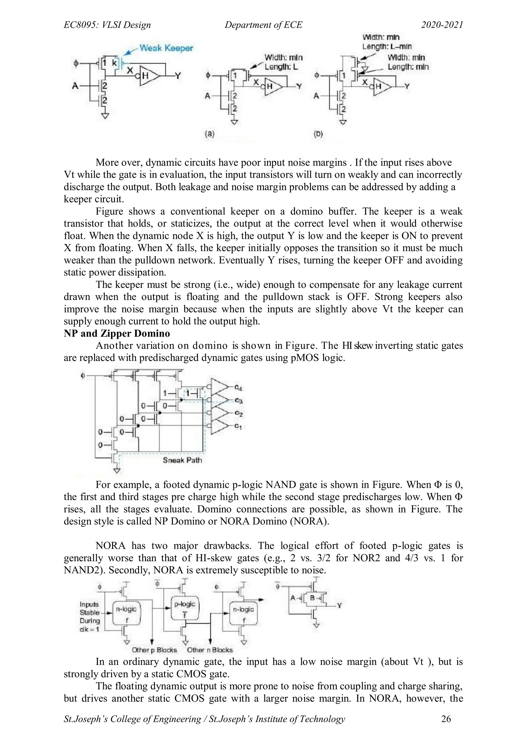
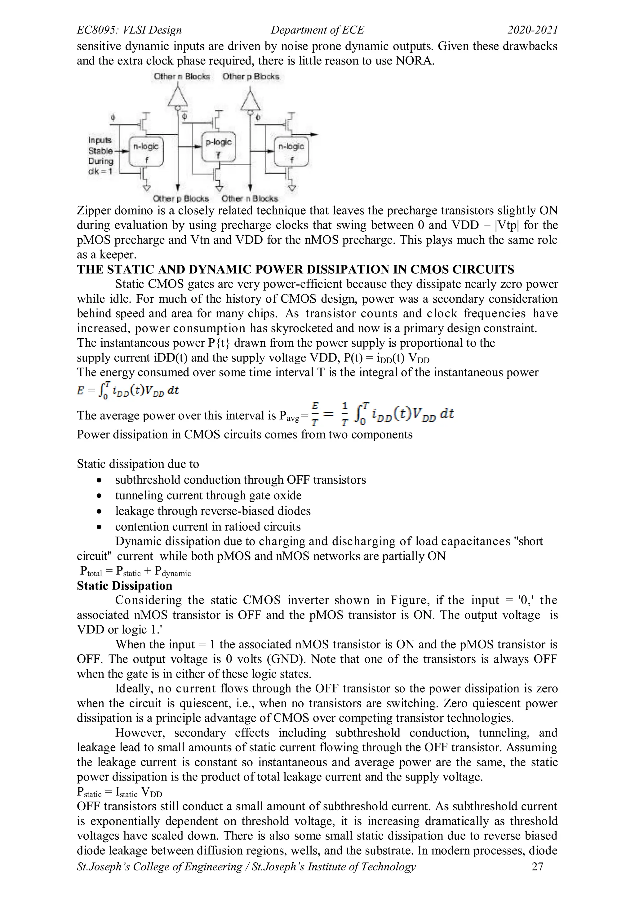
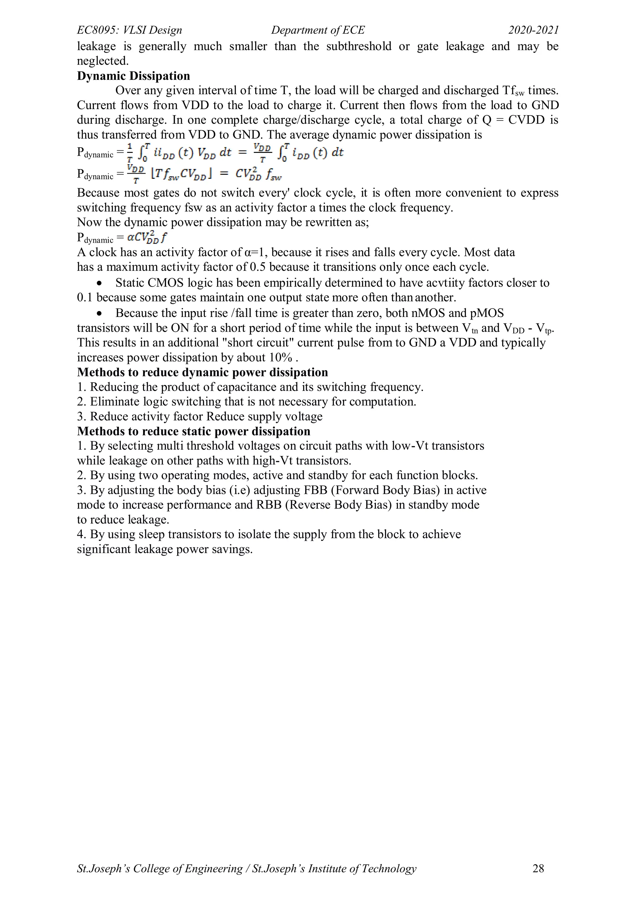
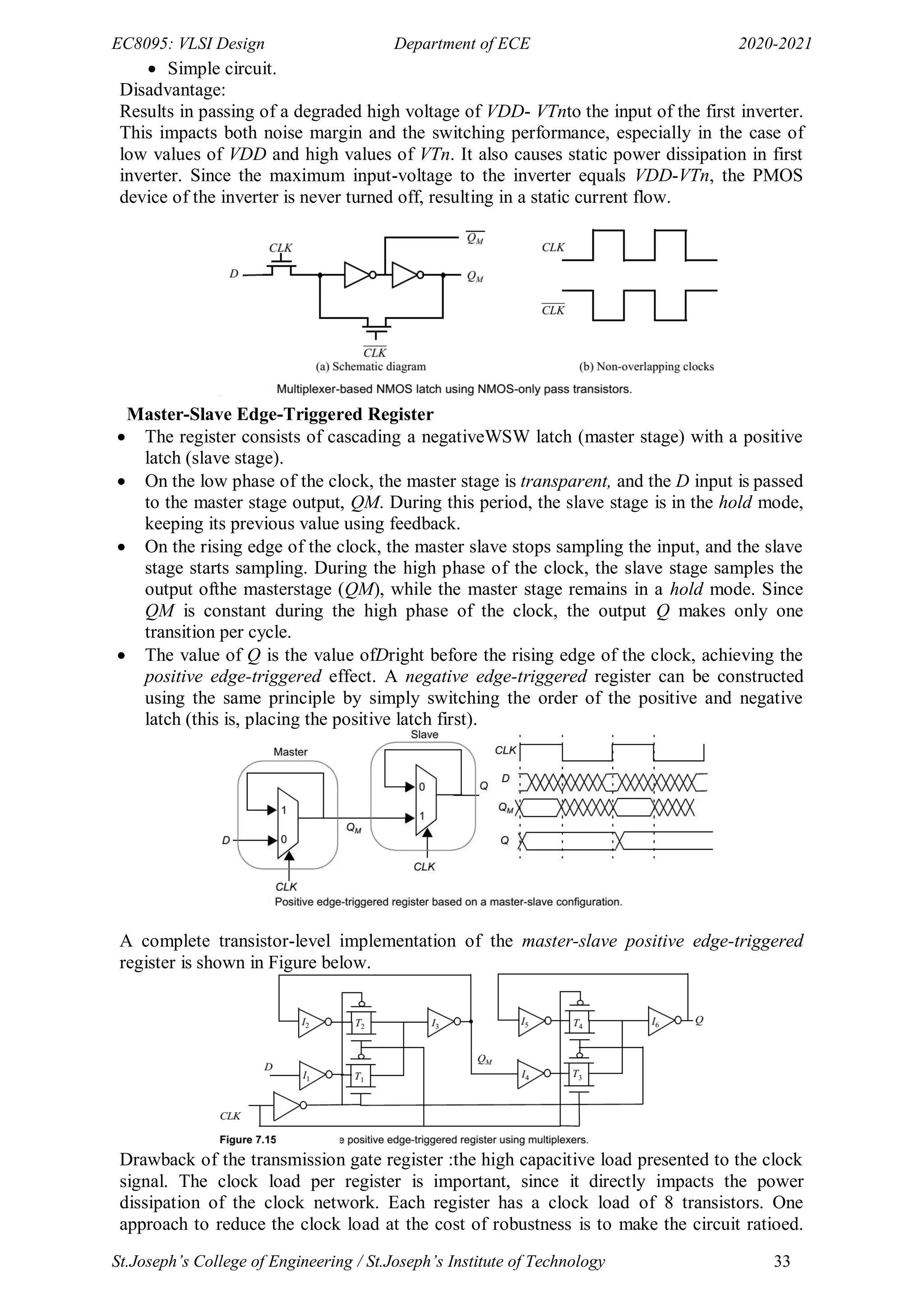
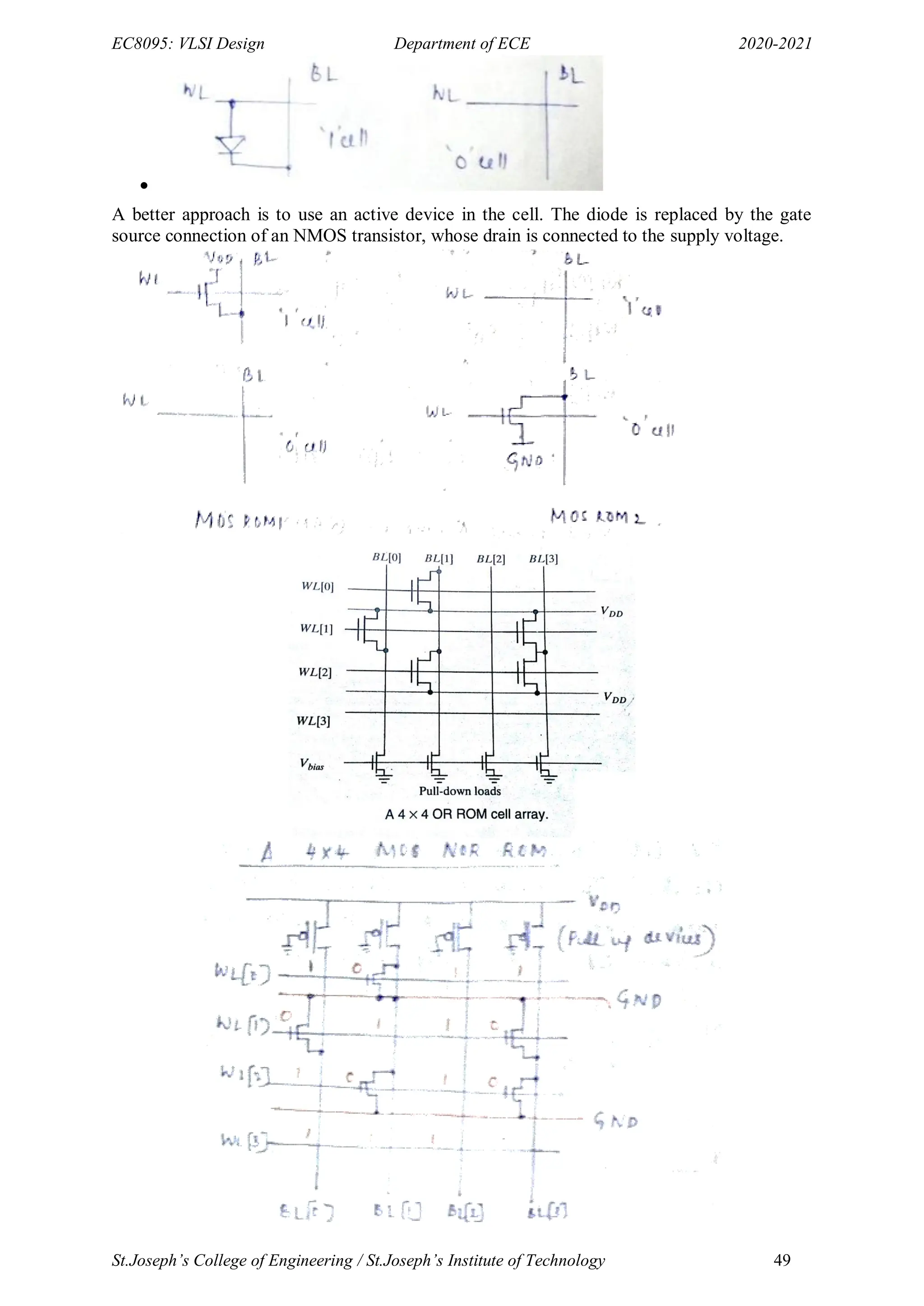
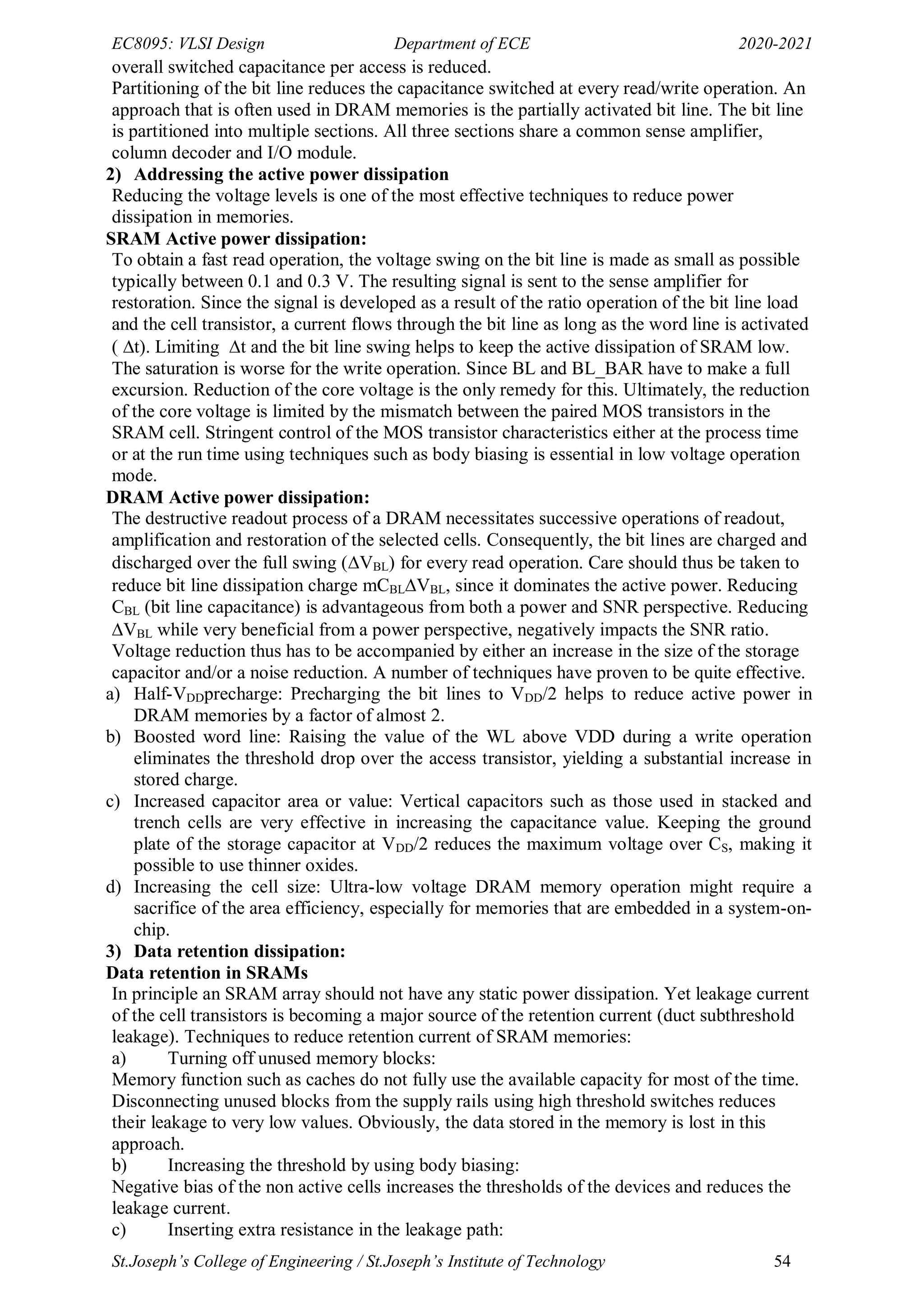
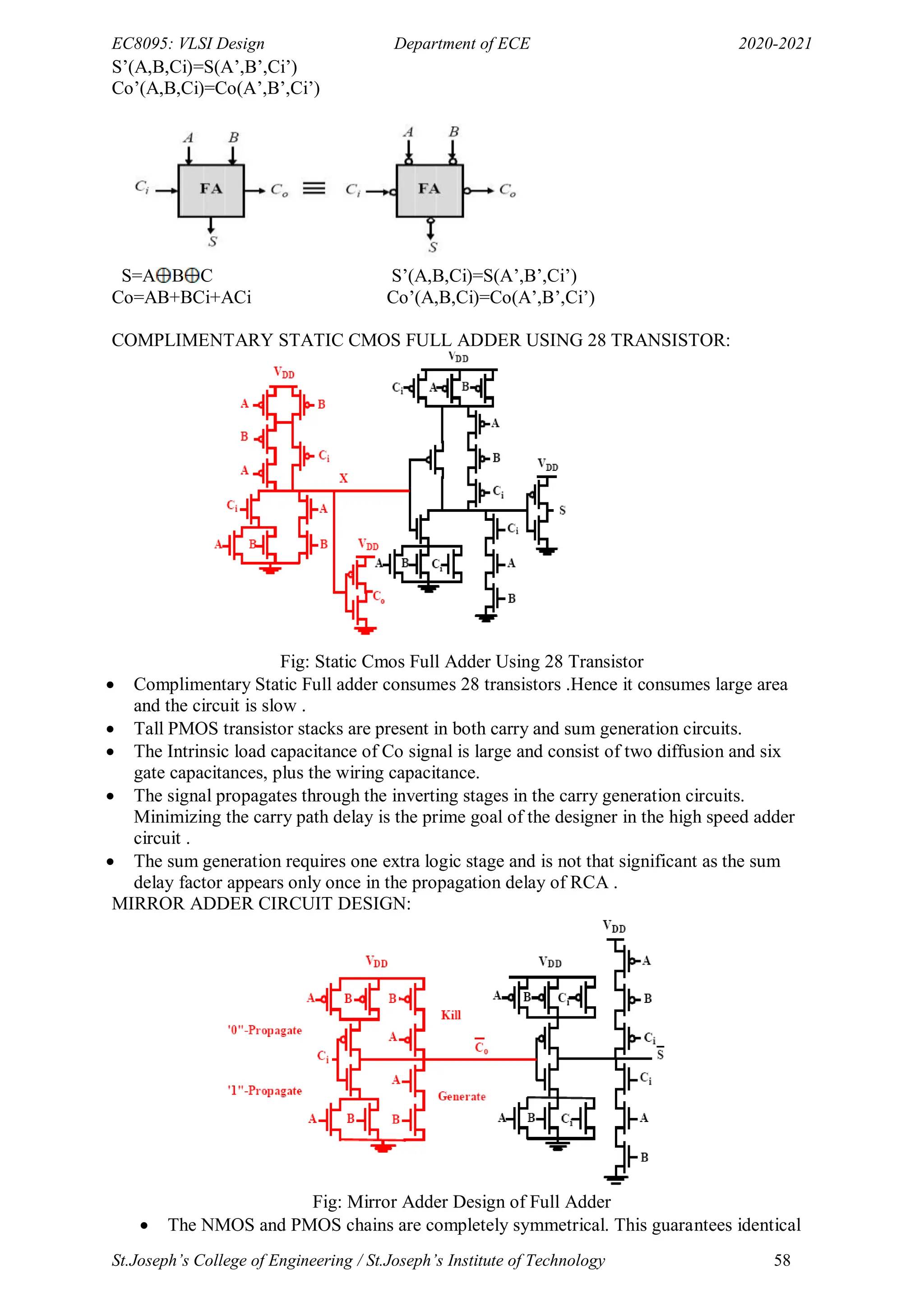
- The document provides an overview of MOS transistor operation and VLSI design fundamentals. It describes the basic MOS transistor structure and components like the gate, source, and drain.
- It explains the different operating regions of MOS transistors like enhancement mode, depletion mode, non-saturated, and saturated regions. Threshold voltage and how it relates to establishing the conducting channel is discussed.
- Effects like mobility degradation and velocity saturation that impact current flow are summarized. Threshold variations due to body effect and drain induced barrier lowering are also covered at a high level.

![EC8095: VLSI Design Department of ECE 2020-2021
St.Joseph’s College of Engineering / St.Joseph’s Institute of Technology 53
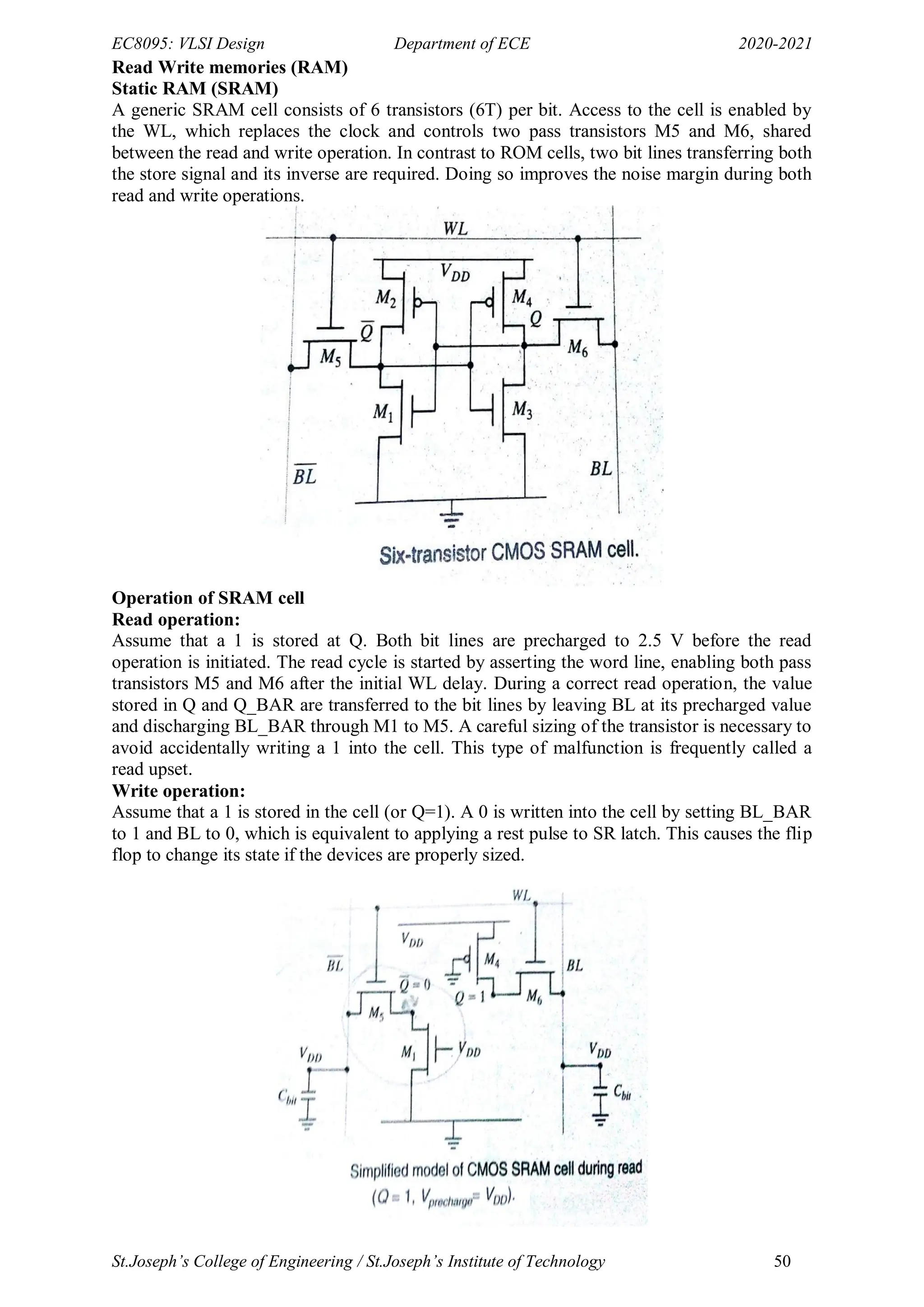
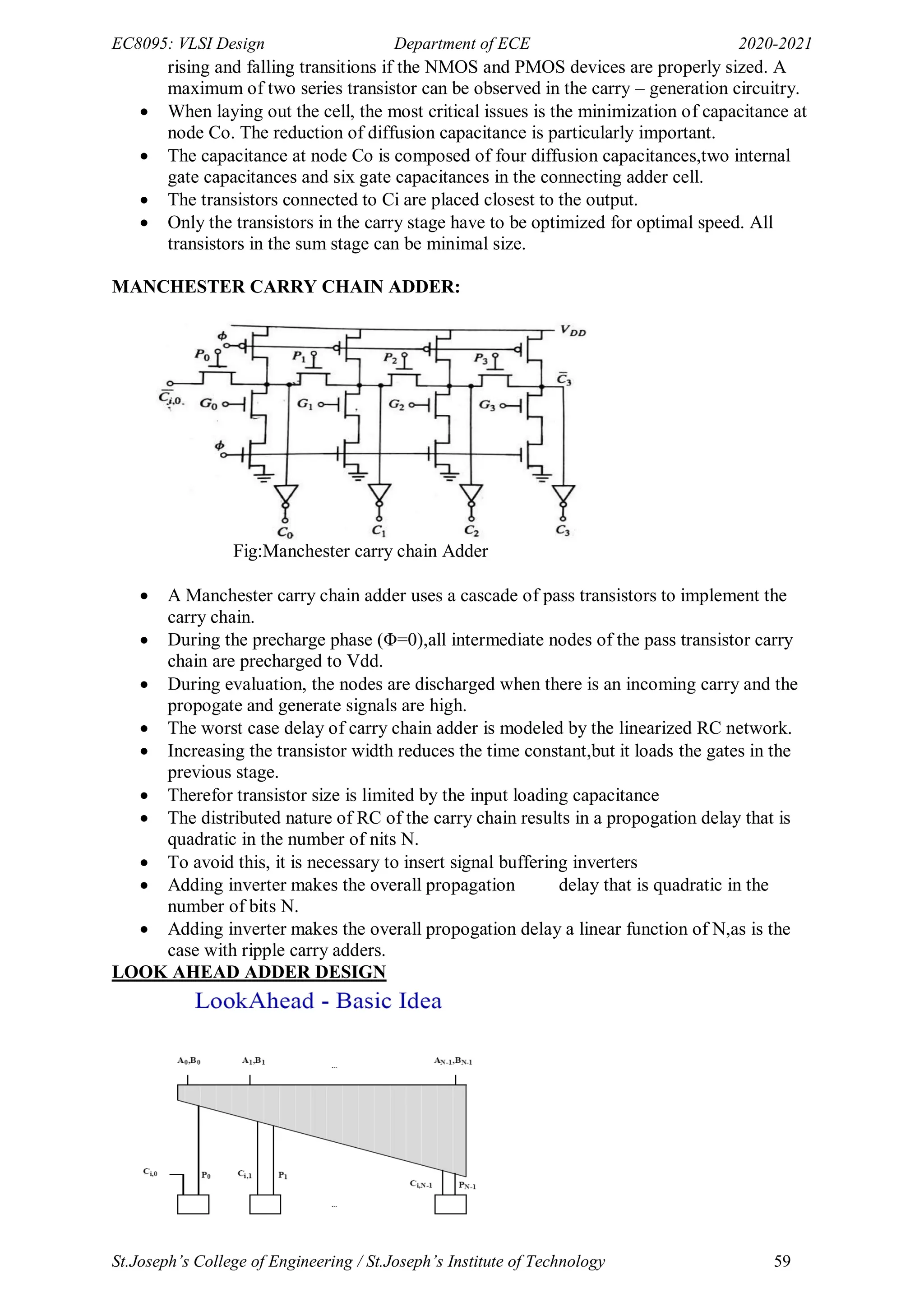
1. Common mode rejection ratio CMRR: ability to amplify the true difference between
the signals and reject the common noise.
2. Power supply rejection ratio PSRR: spikes on the power supply are rejected by this
ratio
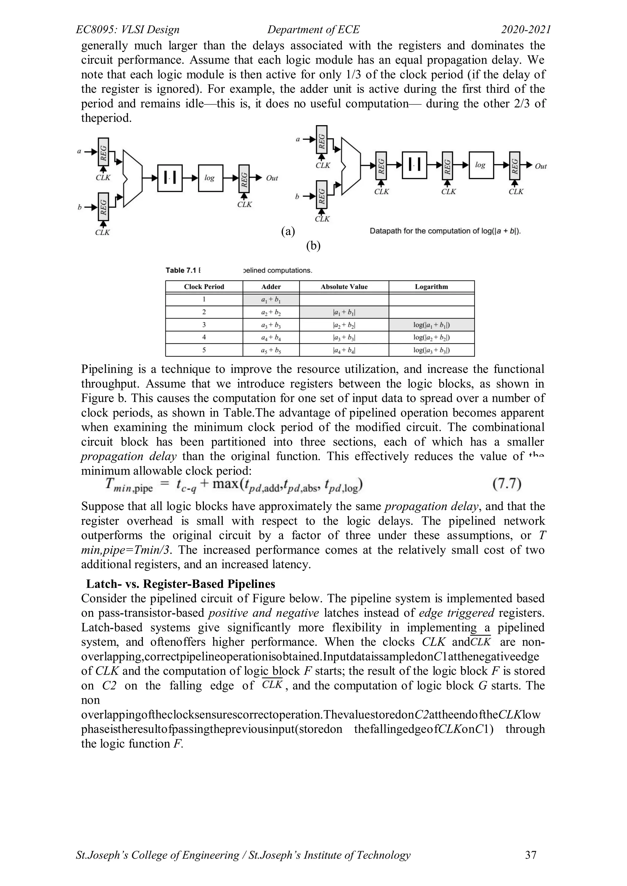
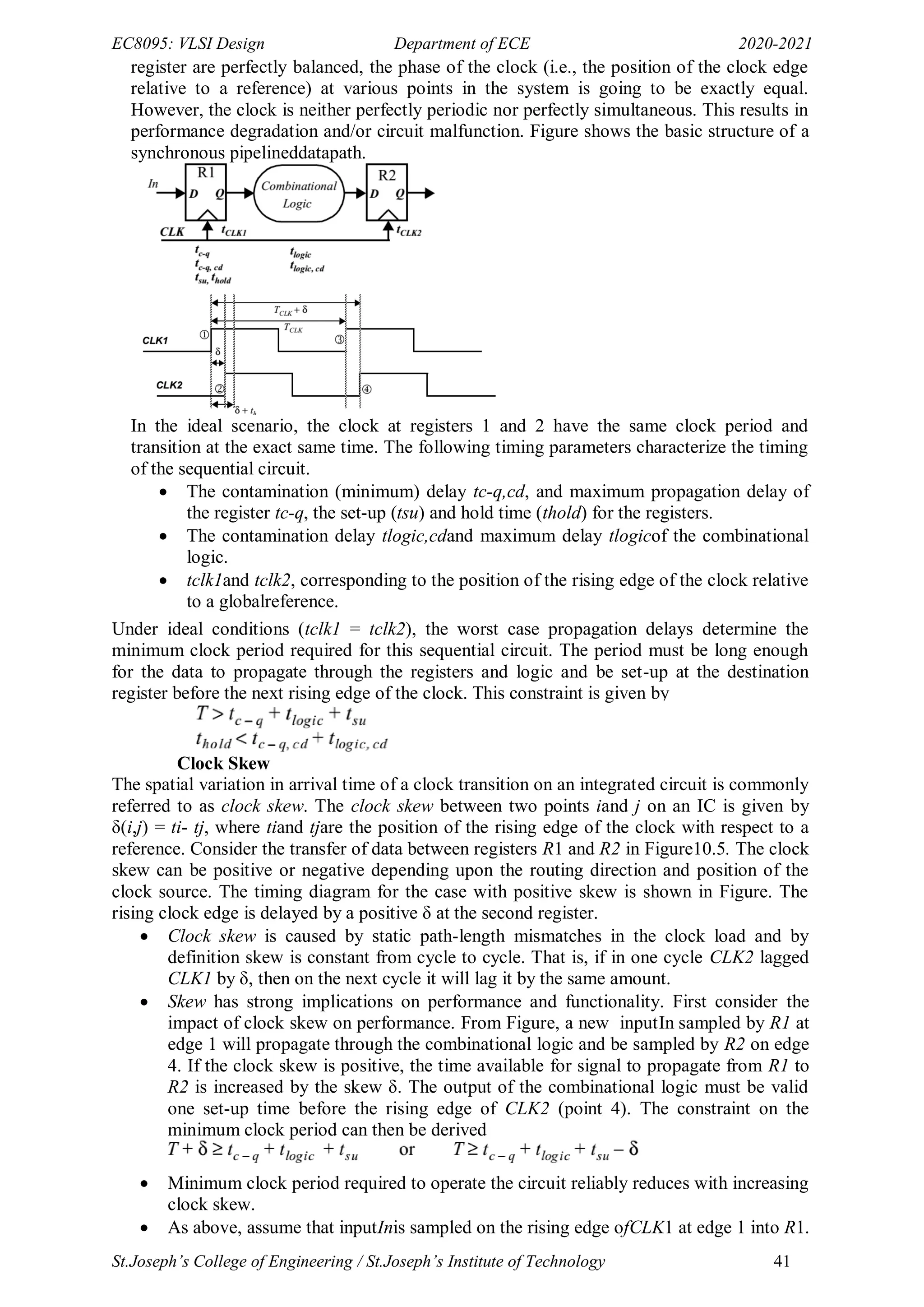
Figure shows the most basic sense amplifier. Amplification is achieved with a single stage,
based on current mirroring concept. The input signals are heavily loaded and driven by the
SRAM memory cell. The swing on those lines is small as the small memory cell drives a
large capacitive load. The inputs are fed to the differential input devices (M1 and M2) and
M3 and M4 act as active current mirror load. The amplifier is conditioned by the sense
amplifier enable signal SE. Initially inputs are precharged and equalized to a common value
while SE is low disabling the circuit. Once the read operation is initiated, one of the bit line
drops, SE is enabled when a sufficient differential signal has been established and the
amplifier evaluates.
Power dissipation in memories:
Reduction of power dissipation in memories is becoming of premier importance. Technology
scaling with its reduction in supply and threshold voltages and its deterioration of the off
current of the transistor causes the standby power of the memory to rise.
Sources of power dissipation in memories:
The power consumption in a memory chip can be attributed to three major sources – the
memory cell array, the decoders (block, row, column) and the periphery. A unified active
power equation for a modern CMOS memory array of m columns and n rows is
approximately given by:
For a normal read cycle
P = VDD IDD
IDD = Iarray + I deocde + I periphery= [miact + m(n-1)ihld] + [(n+m)CDEVintf] + [CPTVintf +
IDCP]
where iact : effective current of the selected or active cells; ihld : the data retention current of
the inactive cells ; CDE: output capacitance of each decoder ;CPT: the total capacitance of the
CMOS logic and peripheral circuits ; Vint: internal supply voltage ; IDCP: the static or
quasistatic current of the periphery. The major source of this current are the sense amplifiers
and the column circuitry. Other sources are the on chip voltage generator; f: operating
frequency
The power dissipation is proportional to the size of the memory. Dividing the memory into
subarrays and keeping n and m small are essential to keep the power within bounds.
In general, the power dissipation of the memory is dominated by the array. The active power
dissipation of the peripheral circuits is small compared to other components. Its standby
power can be high however requiring that circuits such as sense amplifiers are turned off
when not in action. The decoder charging current is also negligibly small in modern RAMs
especially if care is taken that only one out of the n or m nodes is charged at every cycle.
Power reduction Techniques:
1) Partitioning of the memory
A proper division of the memory into submodules goes a long way in confining active power
dissipation to the limited areas of the overall array. Memory units that are not in use should
consume only the power necessary for data retention. Memory portioning is accomplished by
reducing m (the number of cells on a bit line) and/or n (the number of cells on a bit line). By
dividing the word line into several sub word lines that are enabled only when addressed, the](https://image.slidesharecdn.com/vlsi-240322092205-7a65bead/75/vlsi-pdf-important-qzn-answer-for-ece-department-53-2048.jpg)
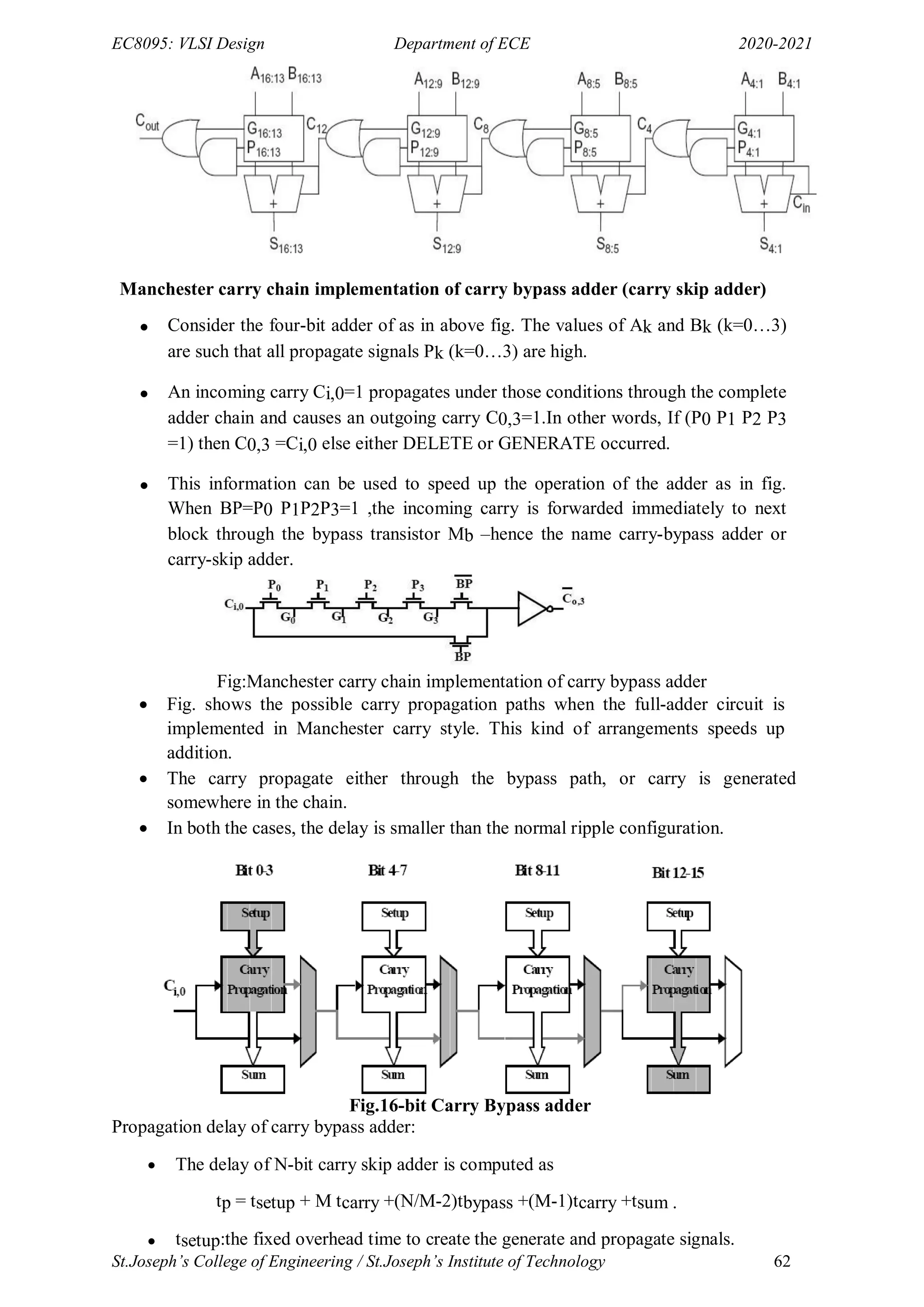
![EC8095: VLSI Design Department of ECE 2020-2021
St.Joseph’s College of Engineering / St.Joseph’s Institute of Technology 61
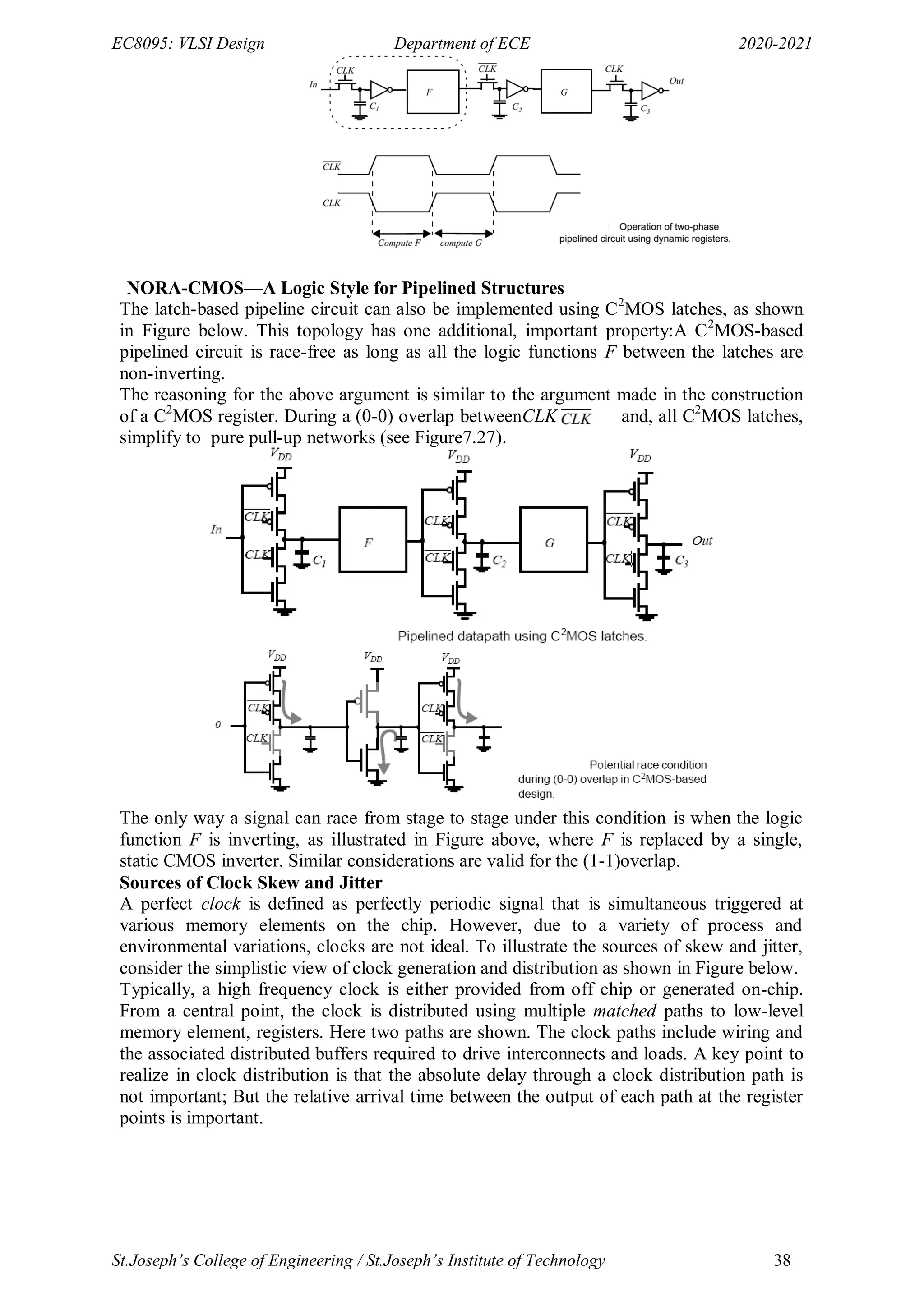
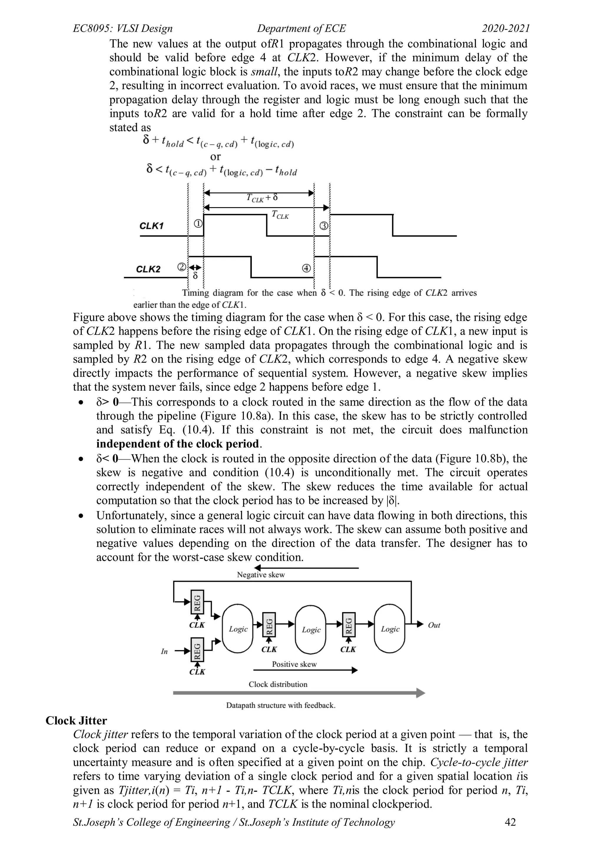
Mirror implementation of Look Ahead Carry Adder
Look-Ahead: Topology
Carry Output equations for 4-bit Look Ahead Adder
c1=Go +c0P0
c2=G1+G0P1+c0P0P1
c3=G2+G1P2+G0P1P2+c0P0P1P2
c4=G3+G2P3+G1P2P3 +G0P1P2P3 +c0P0P1P2P3
4-bit module design
Addition can be reduced to a three-step process:
1. Computing bitwise generate (G) and propagate(P) signals- Bitwise PG logic
2. Combining PG signals to determine group generate(G) and propagate(P) signals-
Group PG Logic
3. Calculating the sums- Sum Logic
Fig: 4-bit Carry Look Ahead Adder Module
16-bit Carry Look Ahead Adder design
In general, a CLA using k groups of n bits each has a delay of
tds = tpg +tpg(n) +[(n-1)+(k-1)]tAO +tXOr](https://image.slidesharecdn.com/vlsi-240322092205-7a65bead/75/vlsi-pdf-important-qzn-answer-for-ece-department-61-2048.jpg)
![EC6601: VLSI Design Department of ECE 2018-19
St. Joseph’s College of Engineering / St. Joseph’s Institute of Technology 65
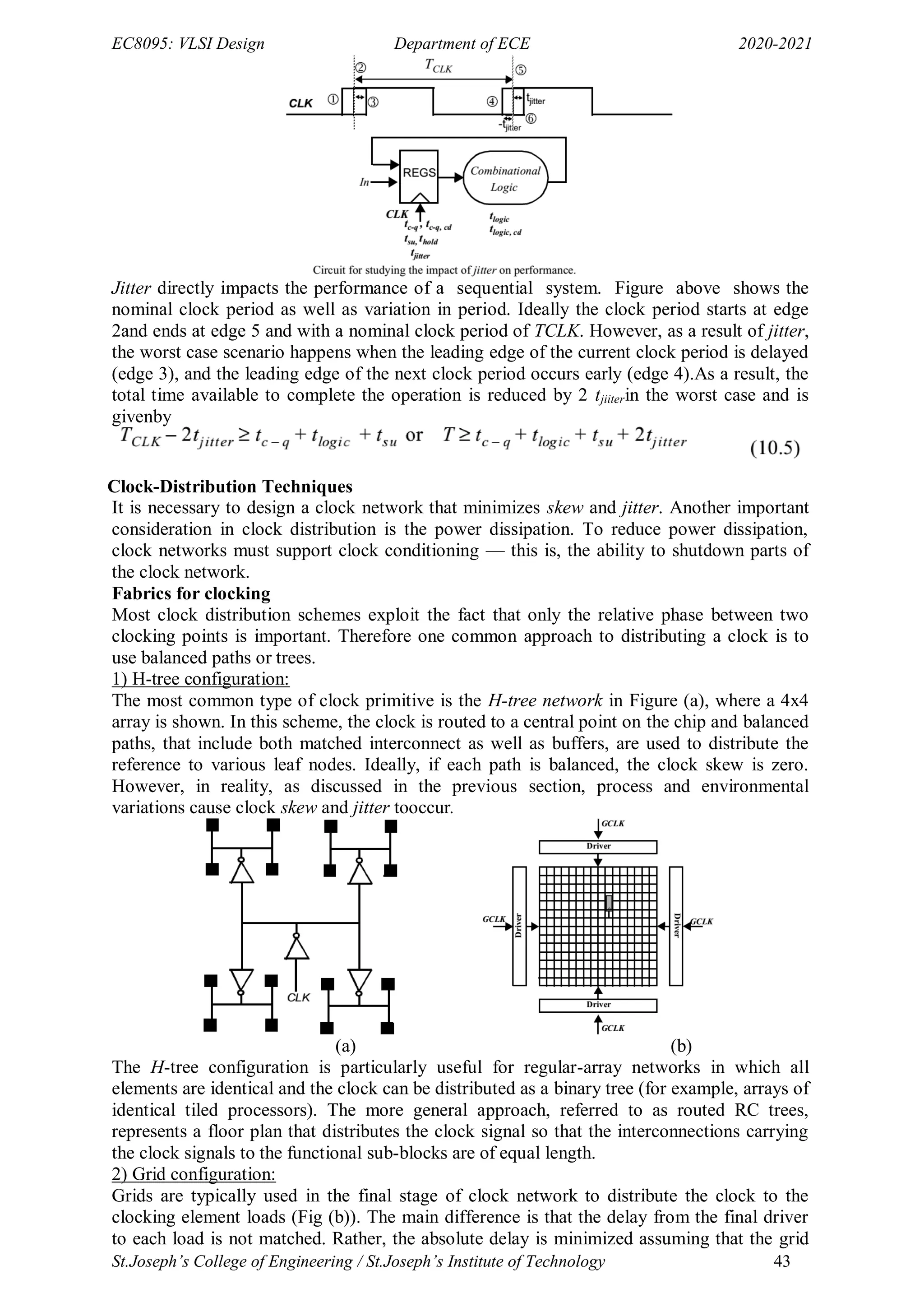
-Leads to less additions with area reduction and higher speed.
-Alternating 10101010 for eight bit is the worst case!
-Multiplying with {-2, -1, 0, 1, 2} versus {1, 0}; needs encoding
-Used modified Booth‘s recoding for consistent operation size.
Modified Booth’sRecoding
Partial product Selection table
Multiplier bits Recorded bits
000 0
001 + Multiplicand
010 + Multiplicand
011 +2 *Multiplicand
100 -2 *Multiplicand
101 -Multiplicand
110 -Multiplicand
111 0
Bunchbitsfrommsbtolsbinthreewithsuccessiveoverlap
Assignmultiplierasperthetable
Numberofpartialproduc
tishalf
Eg.01111111isbunched
into
->01(1), 11(1), 11(1), 11(0)
->Multiplier=10 00 00 01 (see table)
->Four partial product is developed instead]
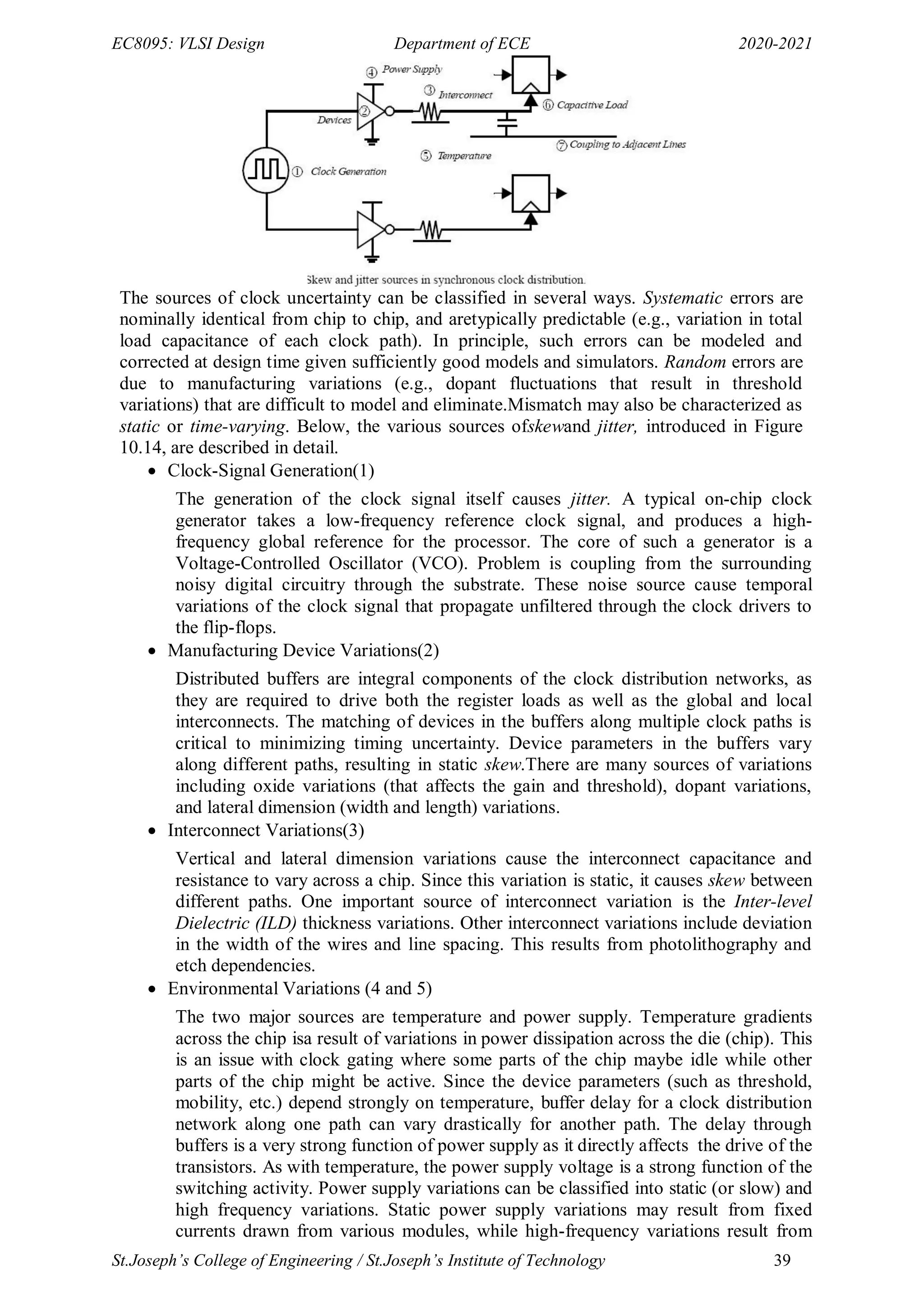
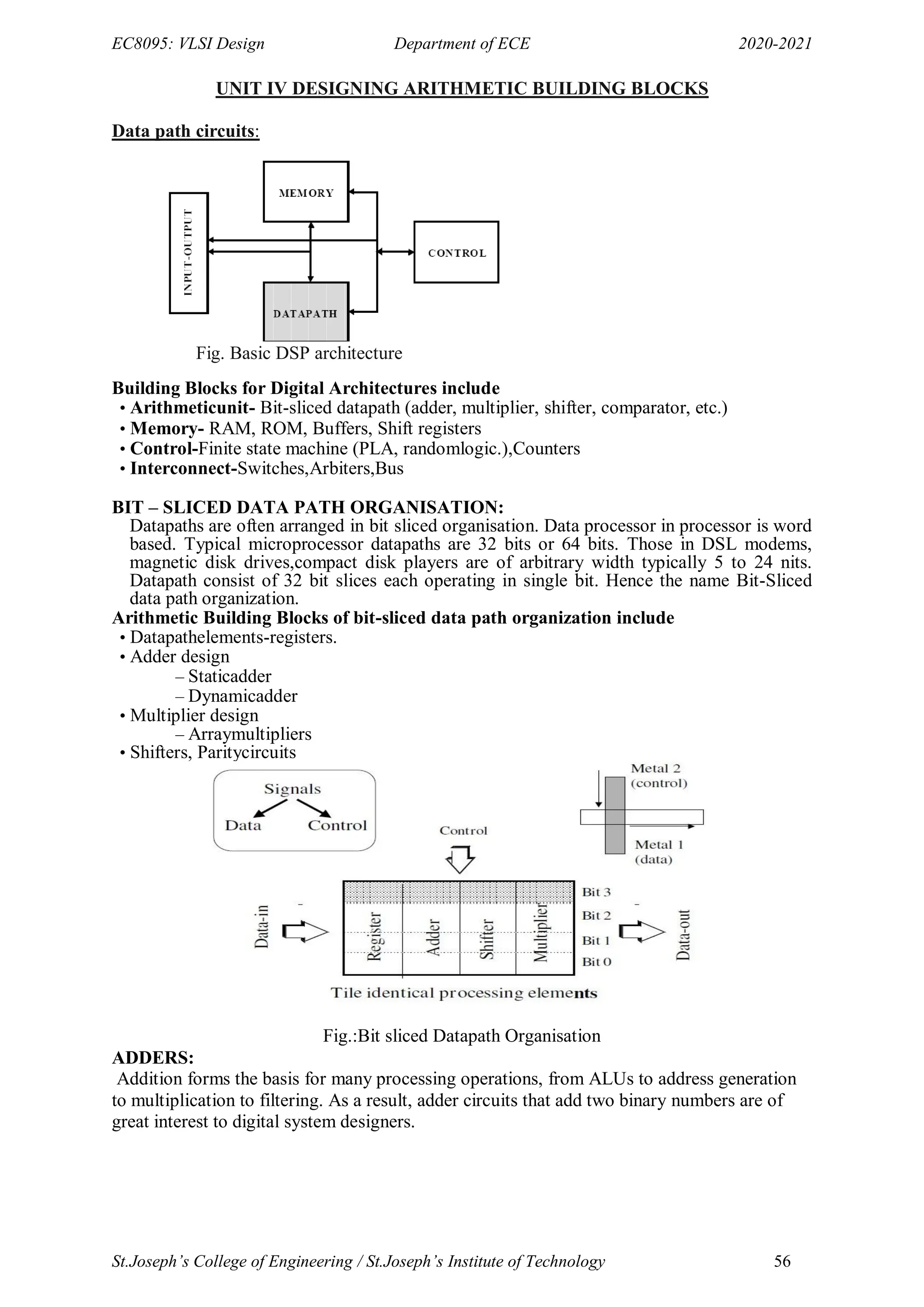
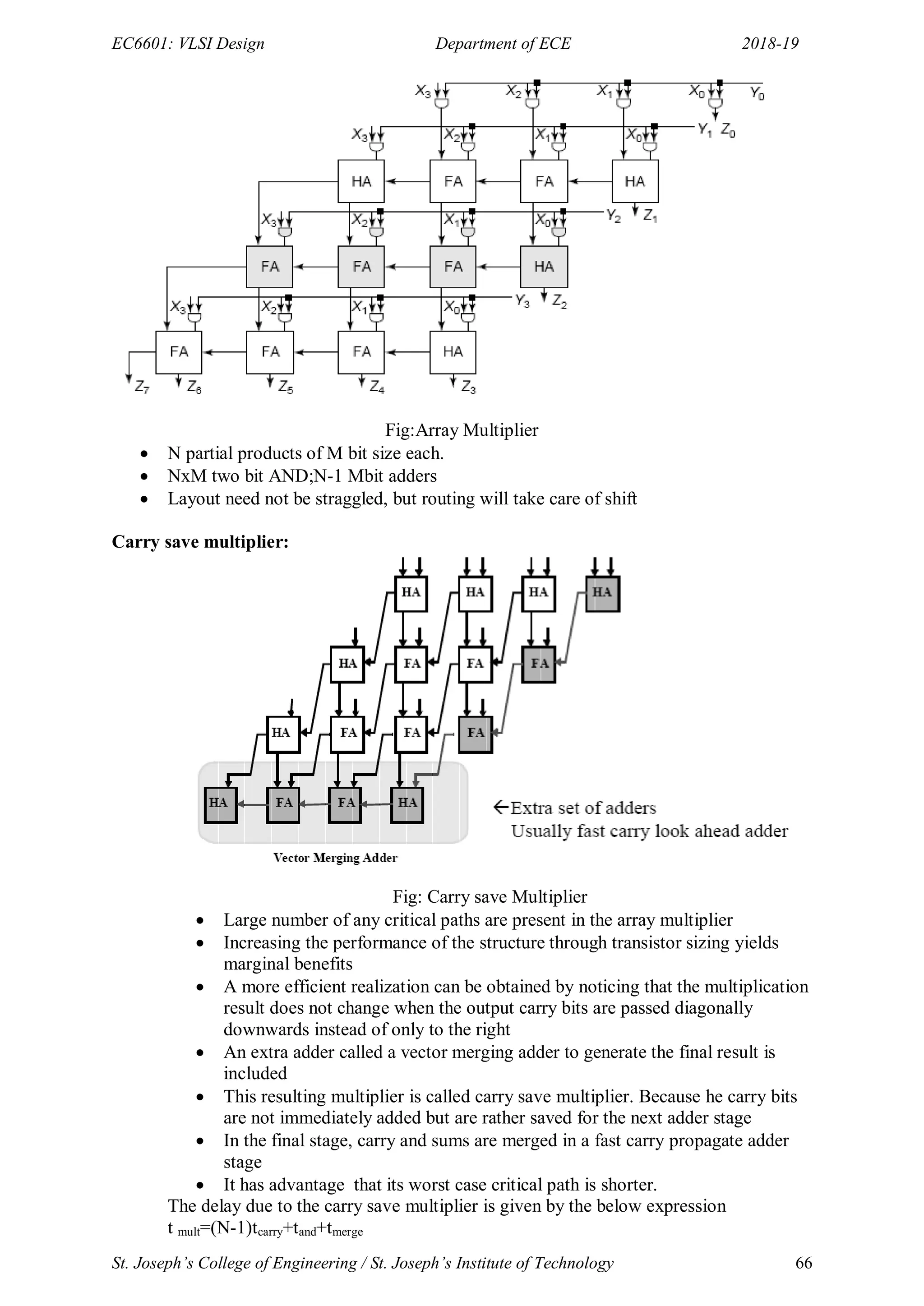
THE ARRAY MULTIPLIER:
An array multiplier is a digital combinational circuit that is used for the multiplication of two
binary numbers by employing an array of full adders and half adders. This array is used for
the nearly simultaneous addition of the various product terms involved.
To form the various product terms, an array of AND gates is used before the Adder array. An
array multiplier is a vast improvement in speed over the traditional bit serial multipliers in
which only one full adder along with a storage memory was used to carry out all the bit
additions involved and also over the row serial multipliers in which product rows (also
known as the partial products) were sequentially added one by one via the use of only one
multi-bit adder.
The tradeoff for this extra speed is the extra hardware required to lay down the adder array.
But with the much decreased costs of these adders, this extra hardware has become quite
affordable to a designer. In spite of the vast improvement in speed, there is still a level of
delay that is involved in an array multiplier before the final product is achieved.Before
committing hardware resources to the circuit, it is important for the designer to calculate the
aforementioned delay in order to make sure that the circuit is compatible with the timing
requirements of the user.](https://image.slidesharecdn.com/vlsi-240322092205-7a65bead/75/vlsi-pdf-important-qzn-answer-for-ece-department-65-2048.jpg)
![EC6601: VLSI Design Department of ECE 2018-19
St. Joseph’s College of Engineering / St. Joseph’s Institute of Technology 68
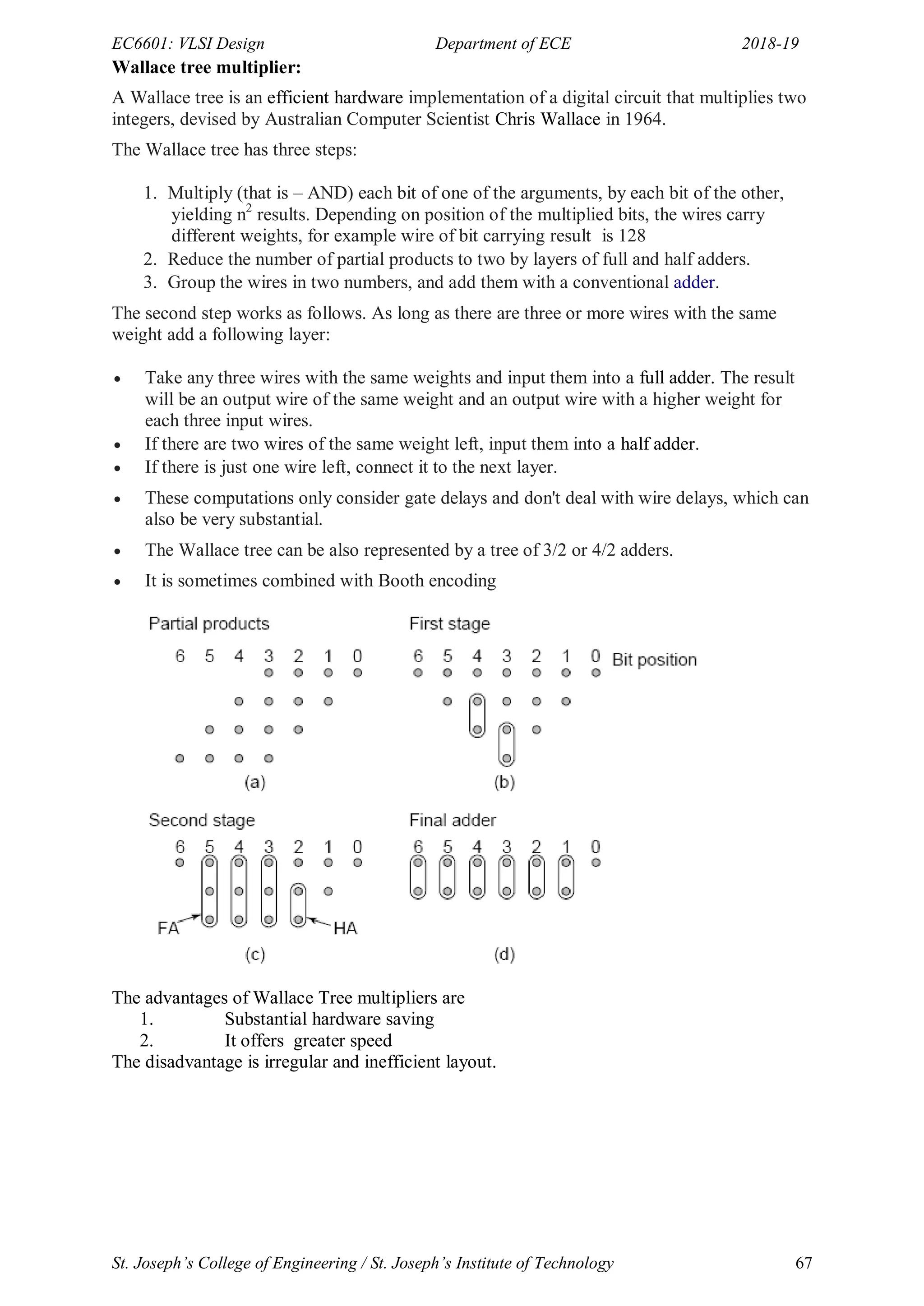
The characteristics of Wallace tree multiplier include
Final adder choice is critical; depends on structure of accumulator array
Carry look ahead might be good if data arrives simultaneously
Place pipeline stage before final addition
In non-pipelined,other adders can be used with similar performance and less
hardware requirement
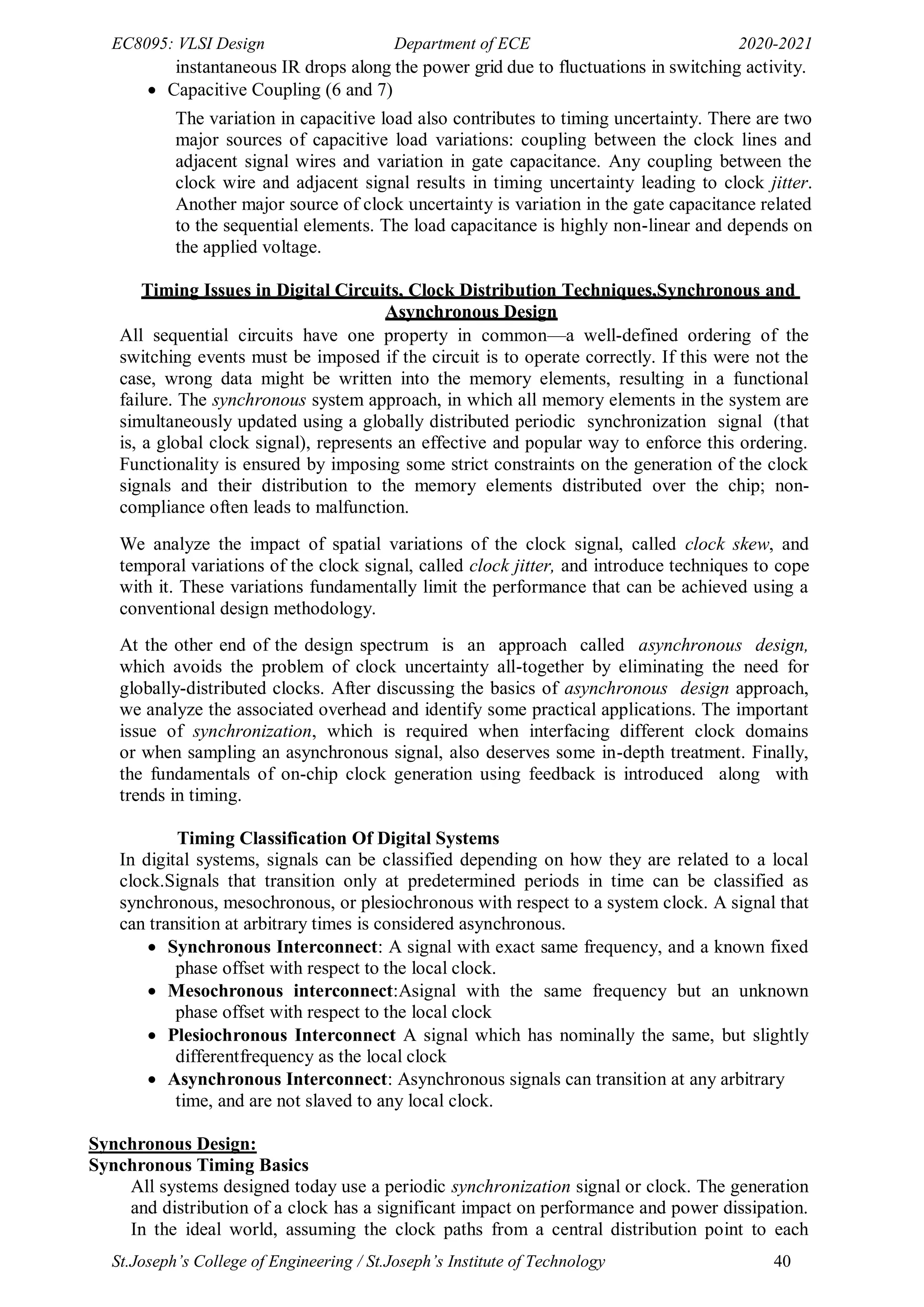
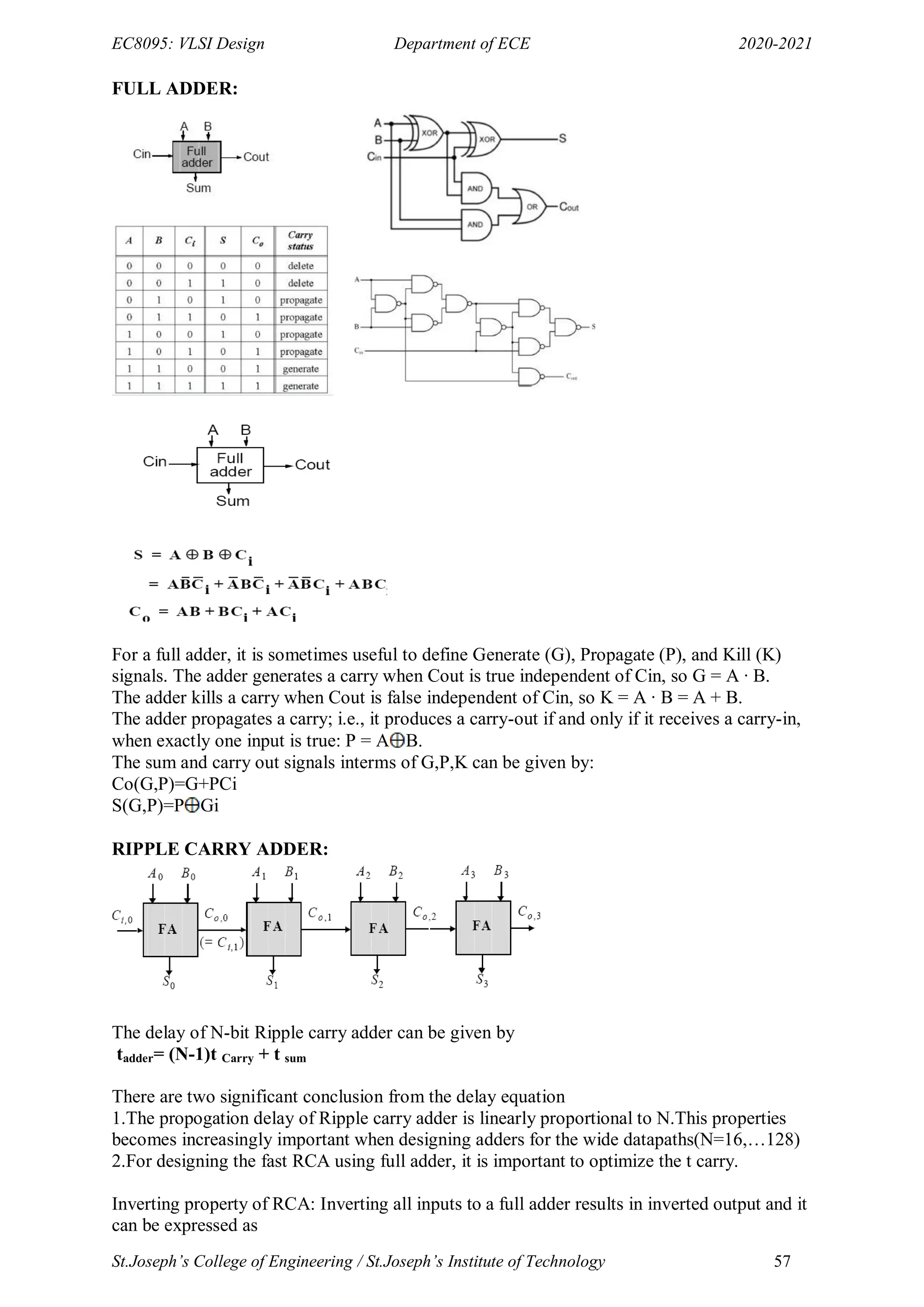
DIVIDER:
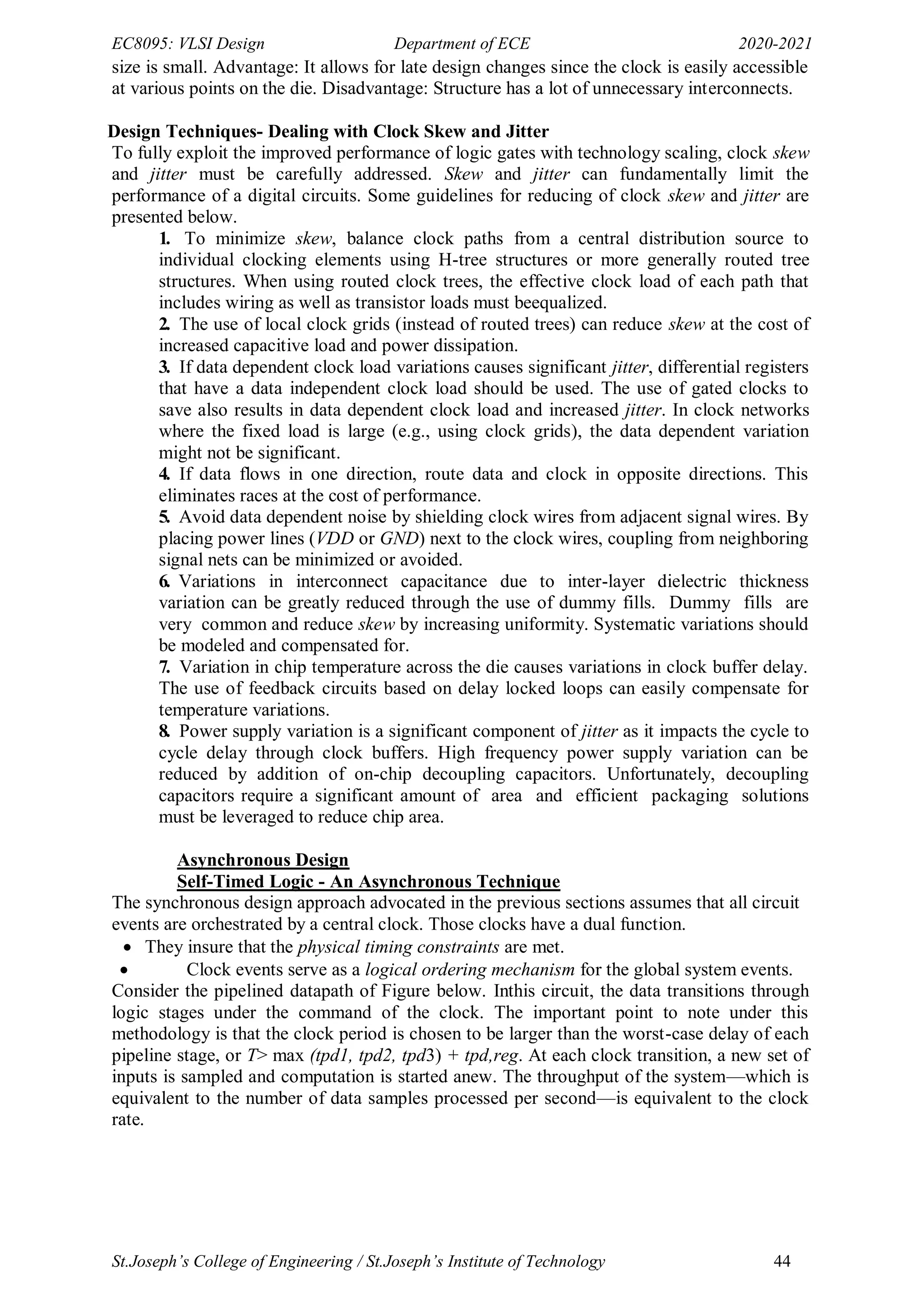
Unsigned non-restoring division:
Input:An n-bit dividend and a m-bit divisor
Output:The quotient and remainder
Begin:
1.load divisor and dividend into regoisters M and D, respectively,clear partial remainder
register R and set loop count cnt equal to n-1.
2.left shift register pair R:D one bit.
3.compute R=R-M;
4.Repeat
If(R<0)begin
D(0)=0;left shift R: D one bit; R=R+M;end
Else begin
D(0)=1 ; let shift R:D one bit ;R=R-M; end
Cnt=cnt-1: until (cnt==0)
5.If(R<0)begin D[0]=0;R=R+M;end else D(0)=1;end
Fig:Sequential Implementation of Non-Restoring Divider.](https://image.slidesharecdn.com/vlsi-240322092205-7a65bead/75/vlsi-pdf-important-qzn-answer-for-ece-department-68-2048.jpg)