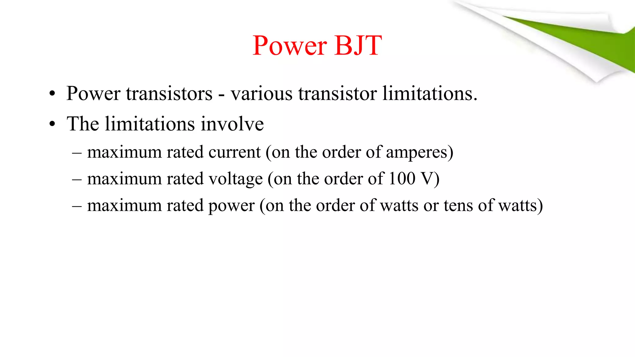
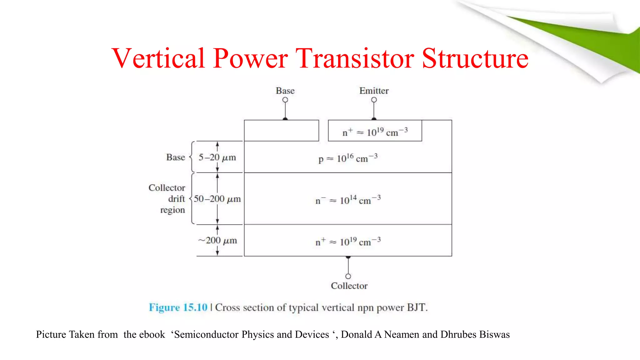
This document discusses power bipolar transistors and power MOSFETs. It describes the vertical structure of power bipolar transistors which allows for higher current handling. Power transistors have lower current gain but larger safe operating areas bounded by maximum current, voltage and power limits to prevent damage. Power MOSFETs provide advantages over bipolar transistors like no second breakdown and stable performance over temperature. They have lower on-resistance and can switch large currents with small control currents. DMOS and VMOS structures are described for power MOSFETs.


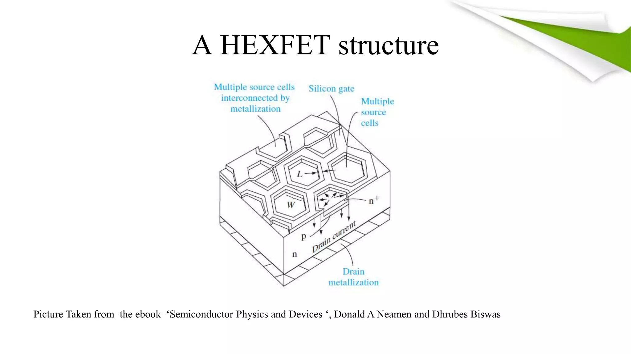
![• Many individual MOSFET cells are connected in parallel to fabricate
a power MOSFET with the proper width-to-length ratio.
• Figure 15.22 shows a HEXFET structure. Each cell is a DMOS
device with an n polysilicon gate.
• The HEXFET has a very high packing density-it may be on the order
of 105 cells per cm2 .
• In the VMOS structure, the anisotropic etching of the grooves must
be along the [110] direction on the (100) surface.
• This constraint limits the design options available for this type of
device.](https://image.slidesharecdn.com/powrbjtandpowermosfet-200523085229/75/Power-BJT-and-Power-MOSFET-22-2048.jpg)