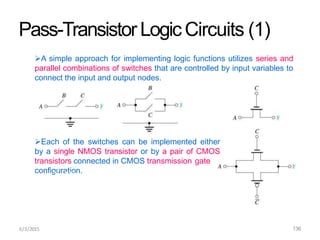
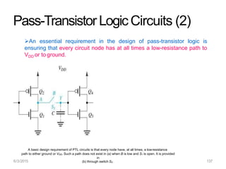
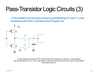
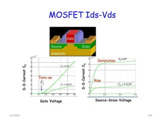
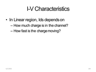
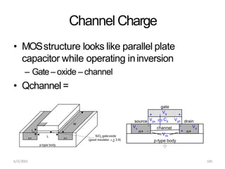
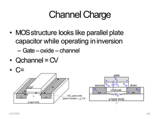
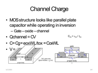
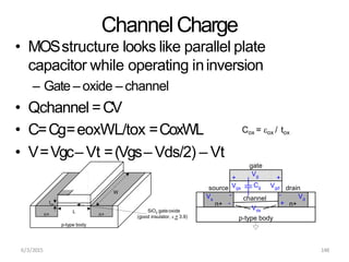
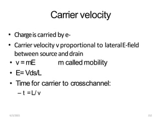
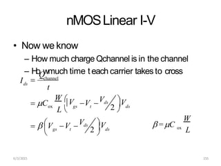
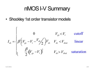
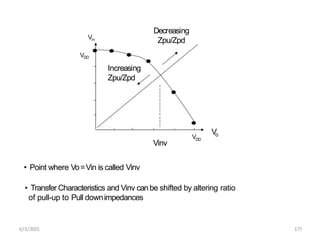
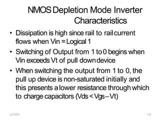
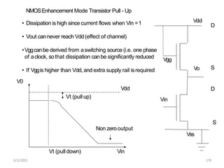
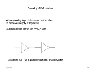
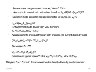
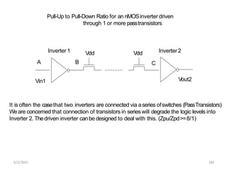
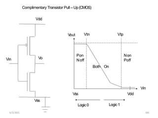
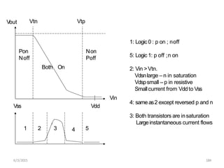
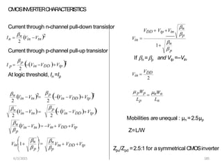
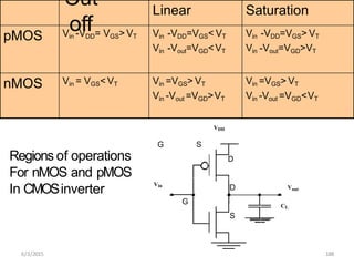
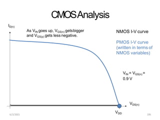
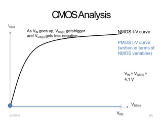
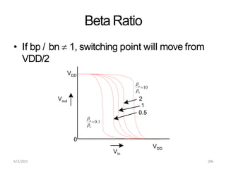
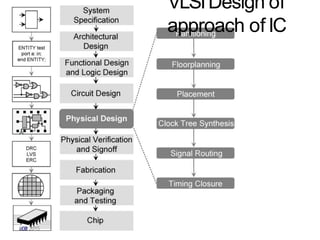
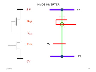
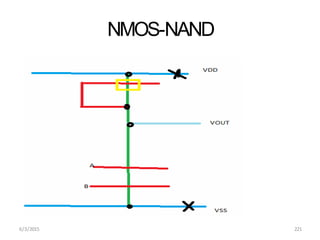
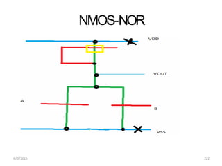
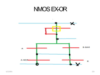
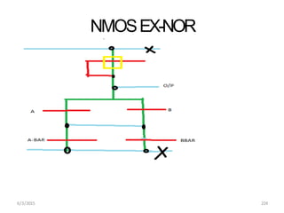
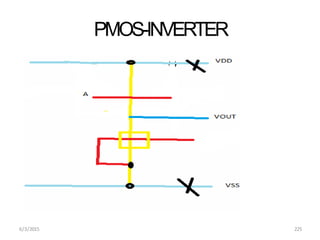
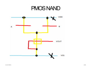
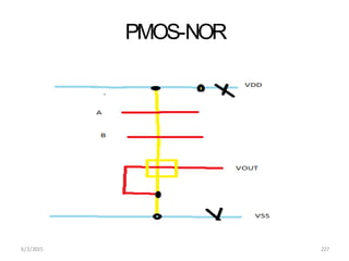
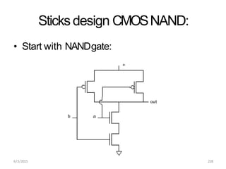
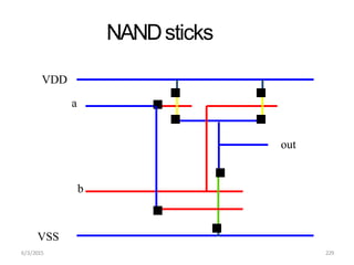
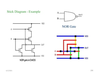
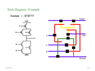
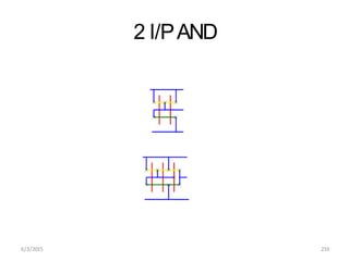
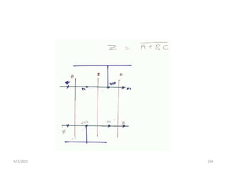
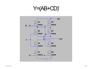
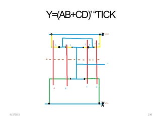
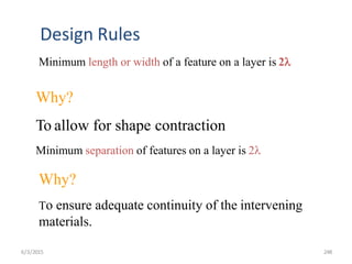
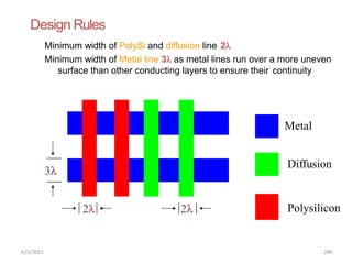
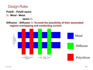
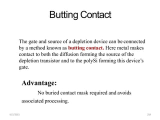
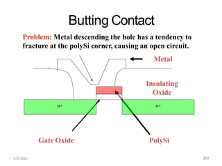
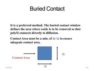
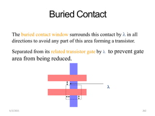
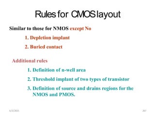
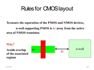
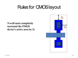
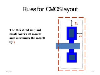
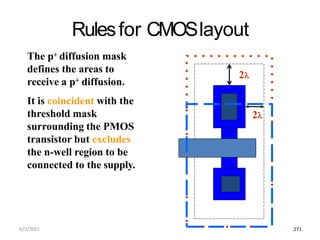
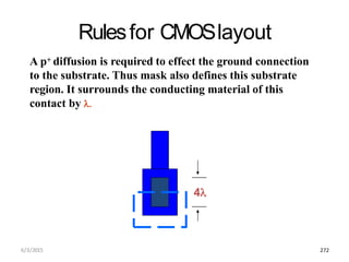
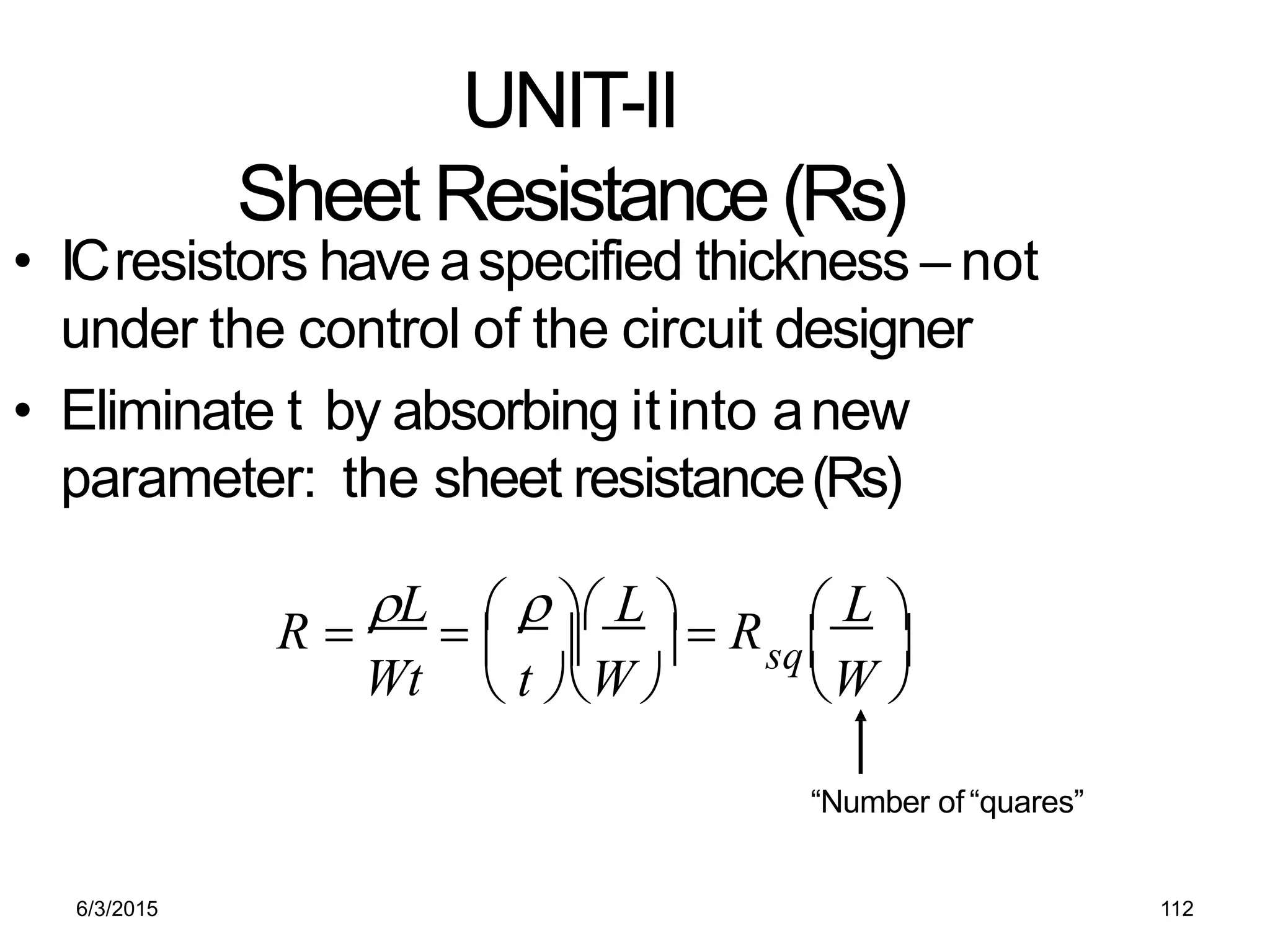
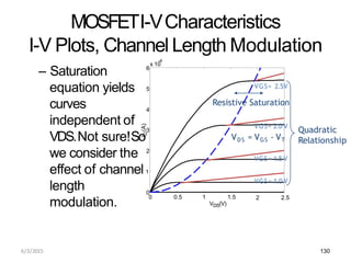
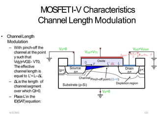
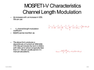
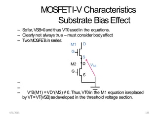
The document discusses the electrical properties and characteristics of MOS and BiCMOS circuits, focusing on parameters such as sheet resistance, channel length modulation, and MOSFET I-V characteristics. It also covers pass-transistor logic circuits and the design requirements for ensuring low-resistance paths in circuit nodes. Additionally, it outlines the operation of NMOS inverters and discusses the impact of various parameters on the device performance.

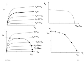
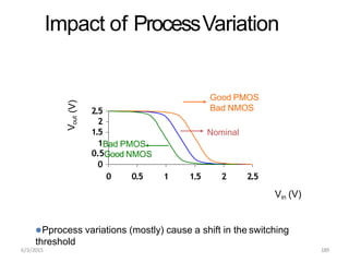
![MOSFETI-V Characteristics
Summary of AnalyticalEquations
– Thevoltage directions and relationships for thethree
modes of pMOSare in contrast to those ofnMOS.
G
D
B
S
VSB VDS
VGS ID
G
S
VDS
VSB
B
VGS
ID
D
nMOS
Mode ID Voltage Range
Cut-off 0 VGS<VT
Linear (µnCox/2)(W/L)[2(VGS
- VT)VDS-VDS
2]
VGSVT,VDS< VGS
-VT
Saturatio
n
(µnCox/2)(W/L)(VGS-
VT)2(1+hVDS)
VGS VT,VDS
VGS -VT
pMOS
Cut-off 0 VGS>VT
Linear (µnCox/2)(W/L)[2(VGS
- VT)VDS-VDS
2]
VGS VT,VDS>
VGS -VT
Saturatio
n
(µnCox/2)(W/L)(VGS-
V )2(1+hV )
VGS VT,VDS135
V -V
6/3/2015](https://image.slidesharecdn.com/vlsi-unit-2-ppt-240717122813-7b1d5057/85/VLSI-UNIT-2-sheet-Resistance-and-Electrical-Properties-8-320.jpg)