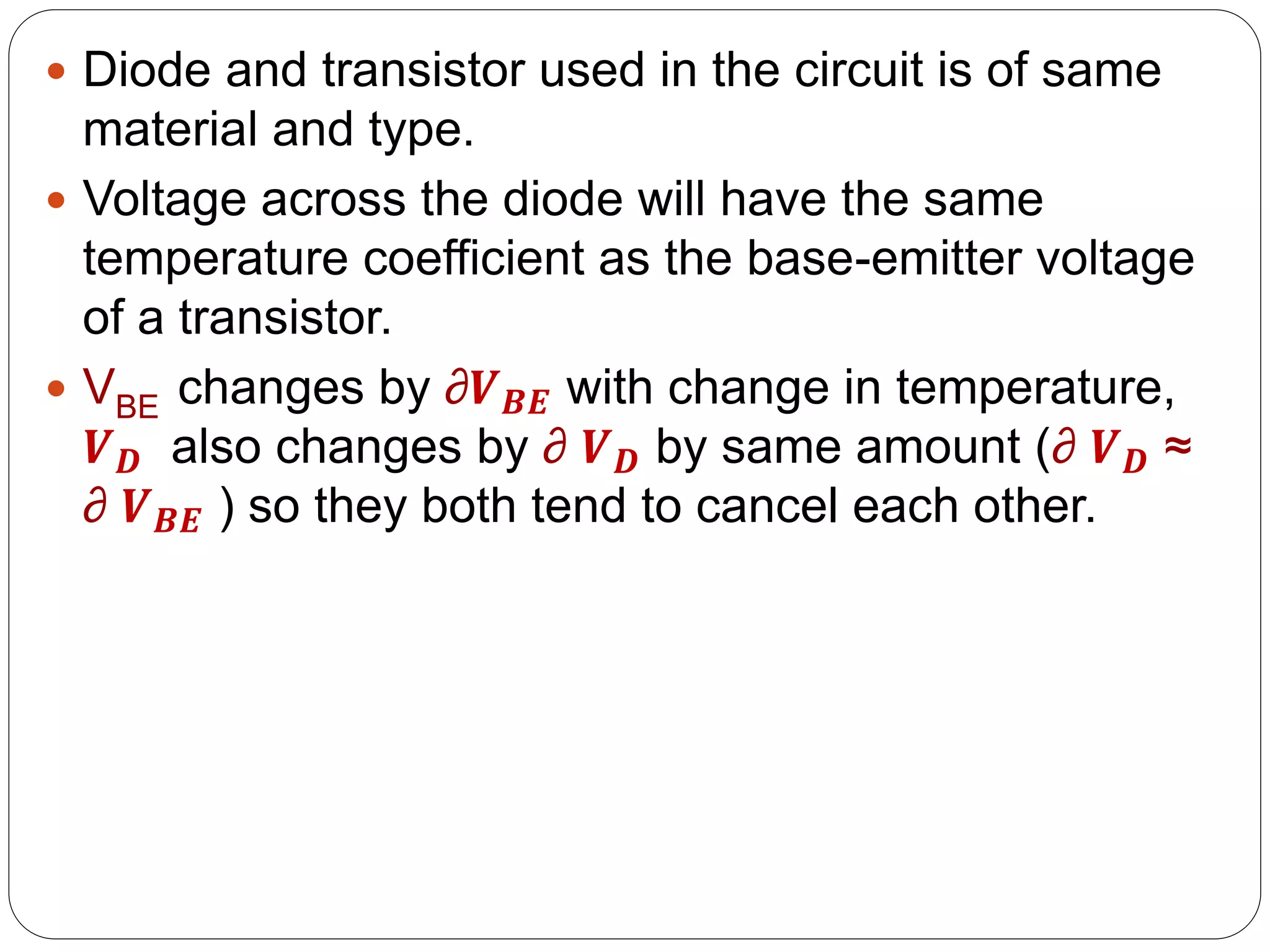
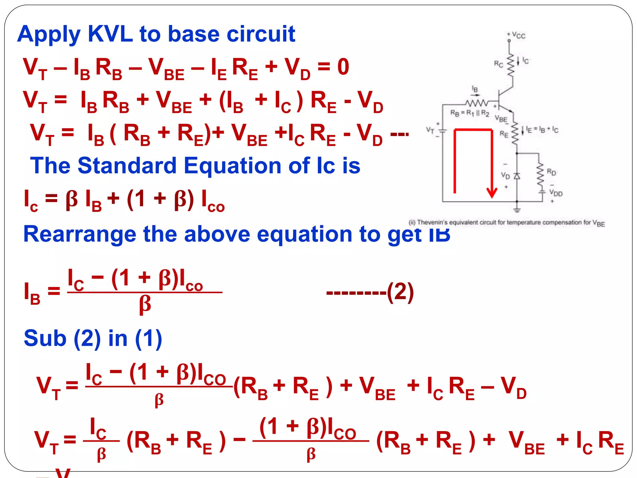
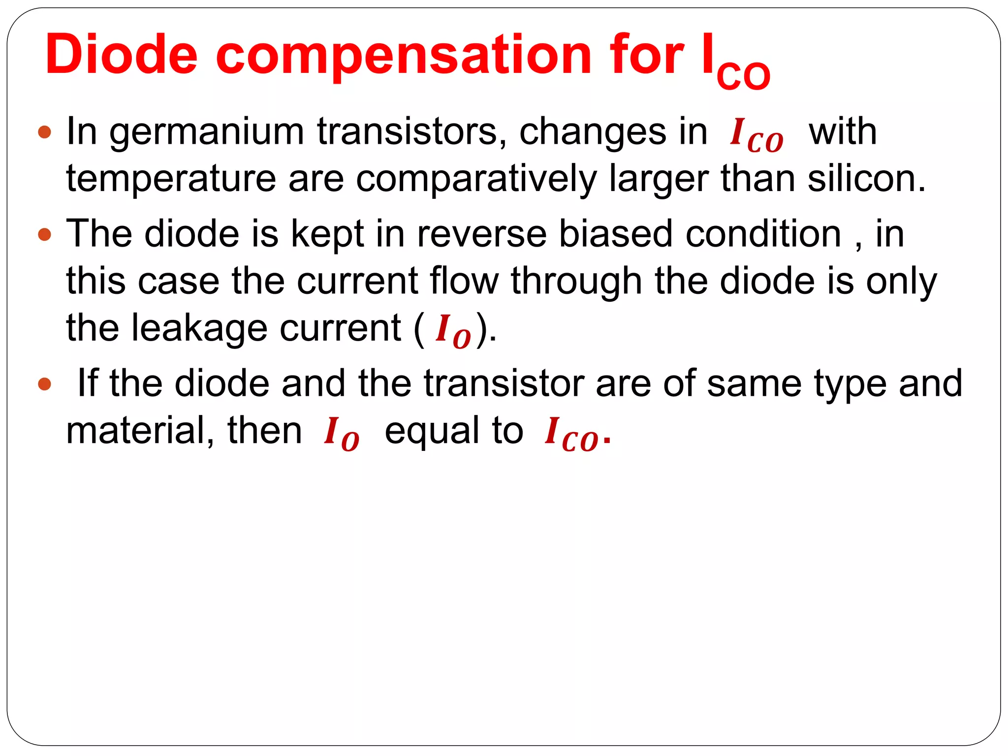
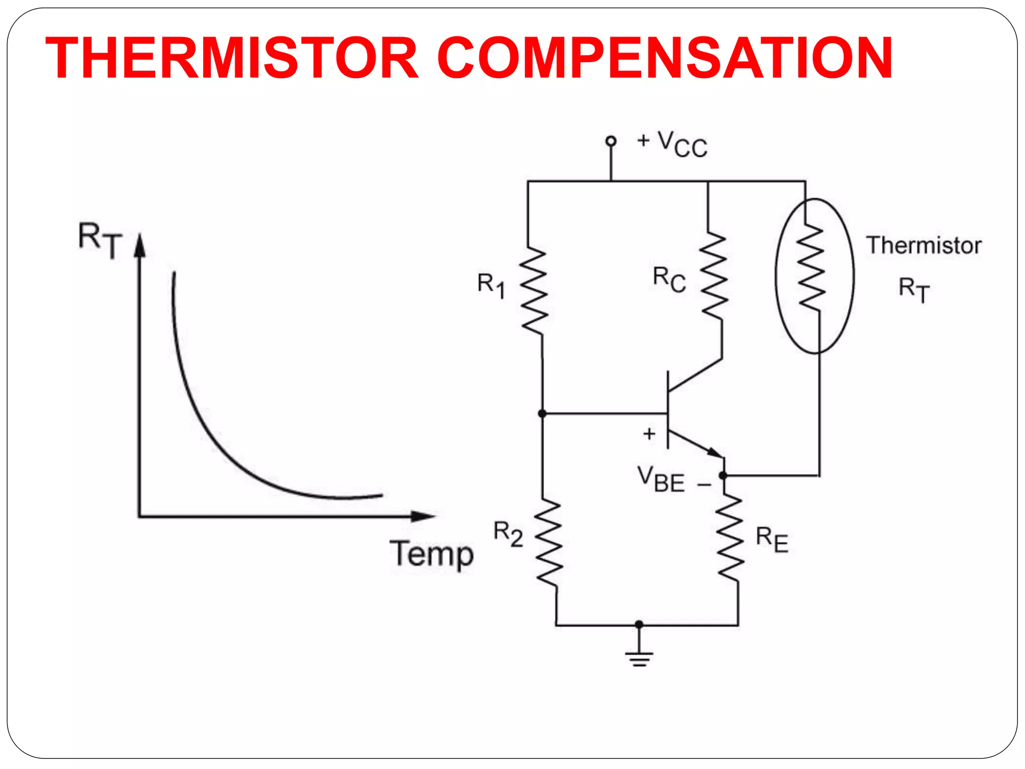
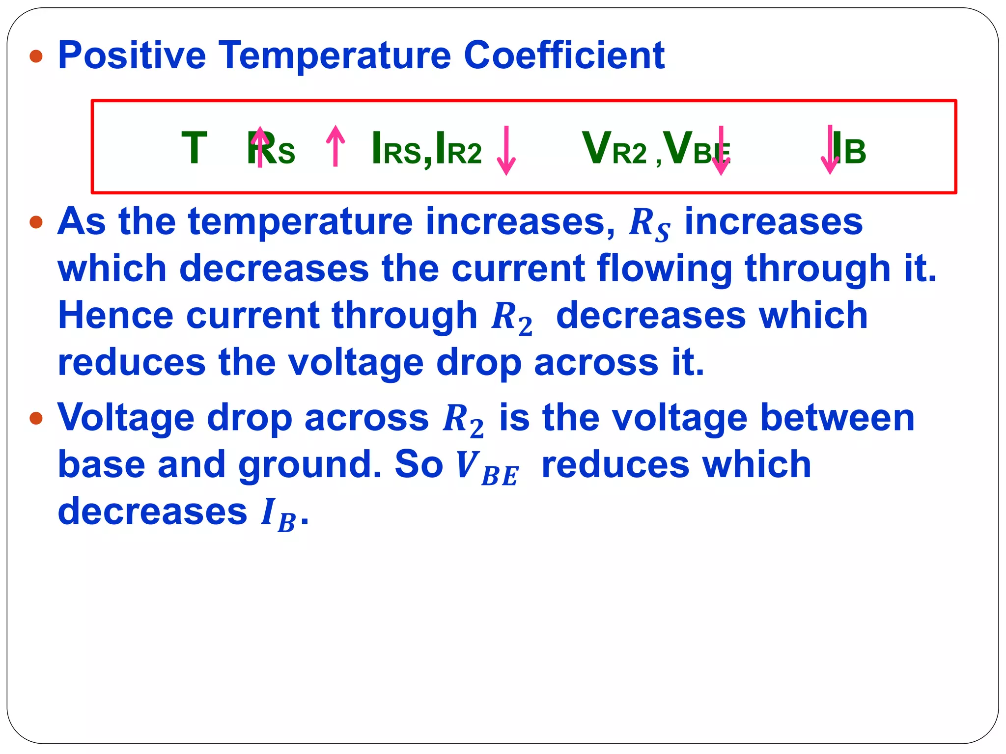
COMPENSATION TECHNIQUES
Dr.N.G.Praveena
Associate Professor/ECE
R.M.K. COLLEGE OF ENGINEERING AND
TECHNOLOGY
TECHNIQUE
 Collector –Base bias and Voltage Divider bias
use the negative feedback to do the stabilization
action.
 Negative feedback reduces the amplification of the
signal.
 To overcome this Compensation Technique are
used which is used to stabilize the Q-point.
 Bias Compensation Methods are
(i) Diode compensation technique
(ii) Thermistor compensation
(iii) Sensistor compensation
Diode Compensation
Technique
 Diode is used as compensation element for
variation in 𝑽𝑩𝑬 𝒐𝒓 𝑰𝑪𝑶.
 For Silicon Diode , the change of 𝑽𝑩𝑬 with
temperature contributes more towards change in 𝑰𝑪
while change in 𝑰𝑪𝑶 is less effective.
 For Germanium Diode, the change of 𝑰𝑪𝑶 with
temperature contributes more towards change in
𝑰𝑪. while change in 𝑽𝑩𝑬 is less effective.
Diode Compensation for VBE
VT = VCC
RB =
 Diode and transistor used in the circuit is of same
material and type.
 Voltage across the diode will have the same
temperature coefficient as the base-emitter voltage
of a transistor.
 VBE changes by ∂𝑽𝑩𝑬 with change in temperature,
𝑽𝑫 also changes by ∂ 𝑽𝑫 by same amount (∂ 𝑽𝑫 ≈
∂ 𝑽𝑩𝑬 ) so they both tend to cancel each other.
Apply KVL to base circuit
VT – IB RB – VBE – IE RE + VD = 0
VT = IB RB + VBE + (IB + IC ) RE - VD
VT = IB ( RB + RE)+ VBE +IC RE - VD ---(1)
The Standard Equation of Ic is
Ic = β IB + (1 + β) Ico
Rearrange the above equation to get IB
IB =
IC − (1 + β)Ico
β
--------(2)
Sub (2) in (1)
VT =
IC − (1 + β)ICO
𝛃
(RB + RE ) + VBE + IC RE – VD
VT =
IC
𝛃
(RB + RE ) −
(1 + β)ICO
𝛃
(RB + RE ) + VBE + IC RE
VT =
IC
𝛃
(RB + RE )−
(1 + β)ICO
𝛃
(RB + RE )+ VBE+IC RE
– VD
VT =
IC
𝛃
[RB +(1+β) RE] −
(1 + β)ICO
𝛃
(RB + RE ) + VBE
– VD
VT =
IC[RB+ (1+β)RE] −(1 + β)ICO(RB+RE )+β(VBE –VD)
β
β VT = IC [RB +(1+β) RE] - (1 + β)ICO (RB + RE ) +β(VBE –VD)
IC [RB +(1+β) RE] = (1 + β)ICO (RB + RE ) +β(VT–VBE+VD)
IC =
(1 + β)ICO(RB+RE ) +β (VT–VBE+VD)
[RB+(1+β)RE]
Diode compensation for ICO
 In germanium transistors, changes in 𝑰𝑪𝑶 with
temperature are comparatively larger than silicon.
 The diode is kept in reverse biased condition , in
this case the current flow through the diode is only
the leakage current ( 𝑰𝑶).
 If the diode and the transistor are of same type and
material, then 𝑰𝑶 equal to 𝑰𝑪𝑶.
Current through resistance R1 can be written as
I =
𝐕𝐂𝐂 −𝐕𝑩𝑬
𝐑𝟏
=
𝑽𝑪𝑪
𝑹𝟏
Apply KCL at node A,
I = IB + Io
IB = I – Io
The standard equation of Ic is
Ic = β IB + (1 + β) Ico
If β >> 1 we get,
Ic = β I – β Io + β Ico
If Io = Ico we get,
IC = β I
A
THERMISTOR COMPENSATION
 Negative Temperature Coefficient
 As the temperature increases, the resistance
𝑹𝑻 decreases. Now the current fed through 𝑹𝑻
into 𝑹𝑬 increases. So the voltage developed
across 𝑹𝑬 increases.
 This voltage reverse-biases the emitter junction
and subtracts from the forward bias provided by
resistors 𝑹𝟏 and 𝑹𝟐. As a result, the collect
current reduces.
T RT IRT,IRE VRE IC
SENSISTOR COMPENSATION
 Positive Temperature Coefficient
 As the temperature increases, 𝑹𝑺 increases
which decreases the current flowing through it.
Hence current through 𝑹𝟐 decreases which
reduces the voltage drop across it.
 Voltage drop across 𝑹𝟐 is the voltage between
base and ground. So 𝑽𝑩𝑬 reduces which
decreases 𝑰𝑩.
T RS IRS,IR2 VR2 ,VBE IB

Compensation Techniques

  • 1.
  • 2.
    TECHNIQUE  Collector –Basebias and Voltage Divider bias use the negative feedback to do the stabilization action.  Negative feedback reduces the amplification of the signal.  To overcome this Compensation Technique are used which is used to stabilize the Q-point.  Bias Compensation Methods are (i) Diode compensation technique (ii) Thermistor compensation (iii) Sensistor compensation
  • 3.
    Diode Compensation Technique  Diodeis used as compensation element for variation in 𝑽𝑩𝑬 𝒐𝒓 𝑰𝑪𝑶.  For Silicon Diode , the change of 𝑽𝑩𝑬 with temperature contributes more towards change in 𝑰𝑪 while change in 𝑰𝑪𝑶 is less effective.  For Germanium Diode, the change of 𝑰𝑪𝑶 with temperature contributes more towards change in 𝑰𝑪. while change in 𝑽𝑩𝑬 is less effective.
  • 4.
    Diode Compensation forVBE VT = VCC RB =
  • 5.
     Diode andtransistor used in the circuit is of same material and type.  Voltage across the diode will have the same temperature coefficient as the base-emitter voltage of a transistor.  VBE changes by ∂𝑽𝑩𝑬 with change in temperature, 𝑽𝑫 also changes by ∂ 𝑽𝑫 by same amount (∂ 𝑽𝑫 ≈ ∂ 𝑽𝑩𝑬 ) so they both tend to cancel each other.
  • 6.
    Apply KVL tobase circuit VT – IB RB – VBE – IE RE + VD = 0 VT = IB RB + VBE + (IB + IC ) RE - VD VT = IB ( RB + RE)+ VBE +IC RE - VD ---(1) The Standard Equation of Ic is Ic = β IB + (1 + β) Ico Rearrange the above equation to get IB IB = IC − (1 + β)Ico β --------(2) Sub (2) in (1) VT = IC − (1 + β)ICO 𝛃 (RB + RE ) + VBE + IC RE – VD VT = IC 𝛃 (RB + RE ) − (1 + β)ICO 𝛃 (RB + RE ) + VBE + IC RE
  • 7.
    VT = IC 𝛃 (RB +RE )− (1 + β)ICO 𝛃 (RB + RE )+ VBE+IC RE – VD VT = IC 𝛃 [RB +(1+β) RE] − (1 + β)ICO 𝛃 (RB + RE ) + VBE – VD VT = IC[RB+ (1+β)RE] −(1 + β)ICO(RB+RE )+β(VBE –VD) β β VT = IC [RB +(1+β) RE] - (1 + β)ICO (RB + RE ) +β(VBE –VD) IC [RB +(1+β) RE] = (1 + β)ICO (RB + RE ) +β(VT–VBE+VD) IC = (1 + β)ICO(RB+RE ) +β (VT–VBE+VD) [RB+(1+β)RE]
  • 8.
    Diode compensation forICO  In germanium transistors, changes in 𝑰𝑪𝑶 with temperature are comparatively larger than silicon.  The diode is kept in reverse biased condition , in this case the current flow through the diode is only the leakage current ( 𝑰𝑶).  If the diode and the transistor are of same type and material, then 𝑰𝑶 equal to 𝑰𝑪𝑶.
  • 9.
    Current through resistanceR1 can be written as I = 𝐕𝐂𝐂 −𝐕𝑩𝑬 𝐑𝟏 = 𝑽𝑪𝑪 𝑹𝟏 Apply KCL at node A, I = IB + Io IB = I – Io The standard equation of Ic is Ic = β IB + (1 + β) Ico If β >> 1 we get, Ic = β I – β Io + β Ico If Io = Ico we get, IC = β I A
  • 10.
  • 11.
     Negative TemperatureCoefficient  As the temperature increases, the resistance 𝑹𝑻 decreases. Now the current fed through 𝑹𝑻 into 𝑹𝑬 increases. So the voltage developed across 𝑹𝑬 increases.  This voltage reverse-biases the emitter junction and subtracts from the forward bias provided by resistors 𝑹𝟏 and 𝑹𝟐. As a result, the collect current reduces. T RT IRT,IRE VRE IC
  • 12.
  • 13.
     Positive TemperatureCoefficient  As the temperature increases, 𝑹𝑺 increases which decreases the current flowing through it. Hence current through 𝑹𝟐 decreases which reduces the voltage drop across it.  Voltage drop across 𝑹𝟐 is the voltage between base and ground. So 𝑽𝑩𝑬 reduces which decreases 𝑰𝑩. T RS IRS,IR2 VR2 ,VBE IB