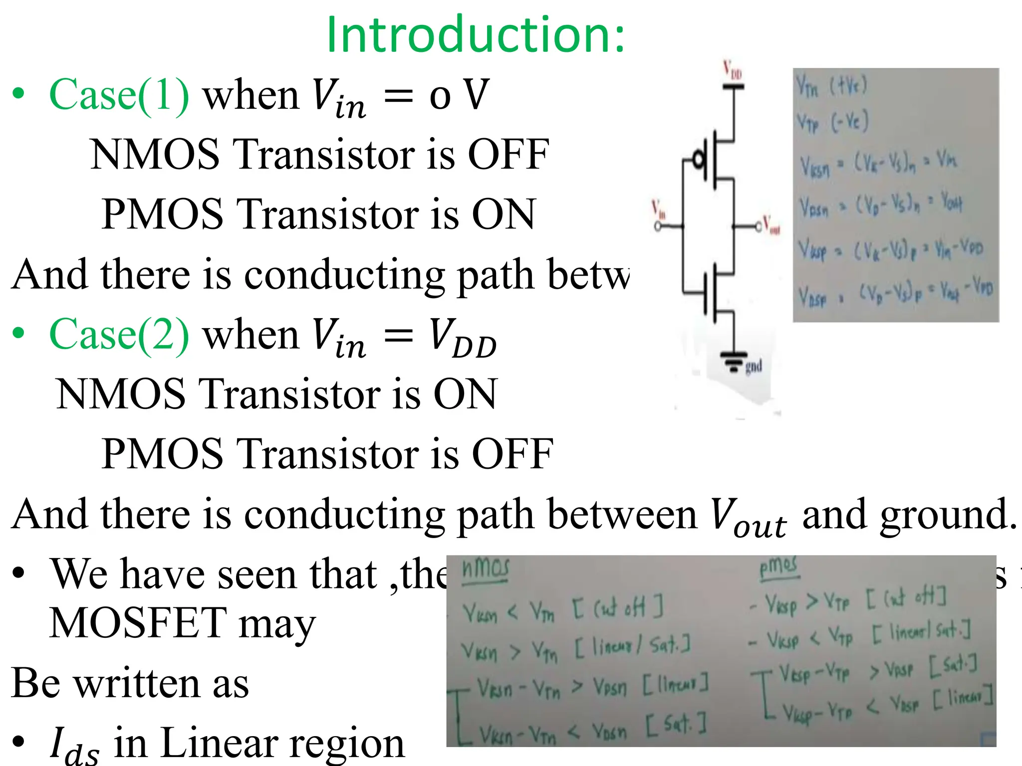
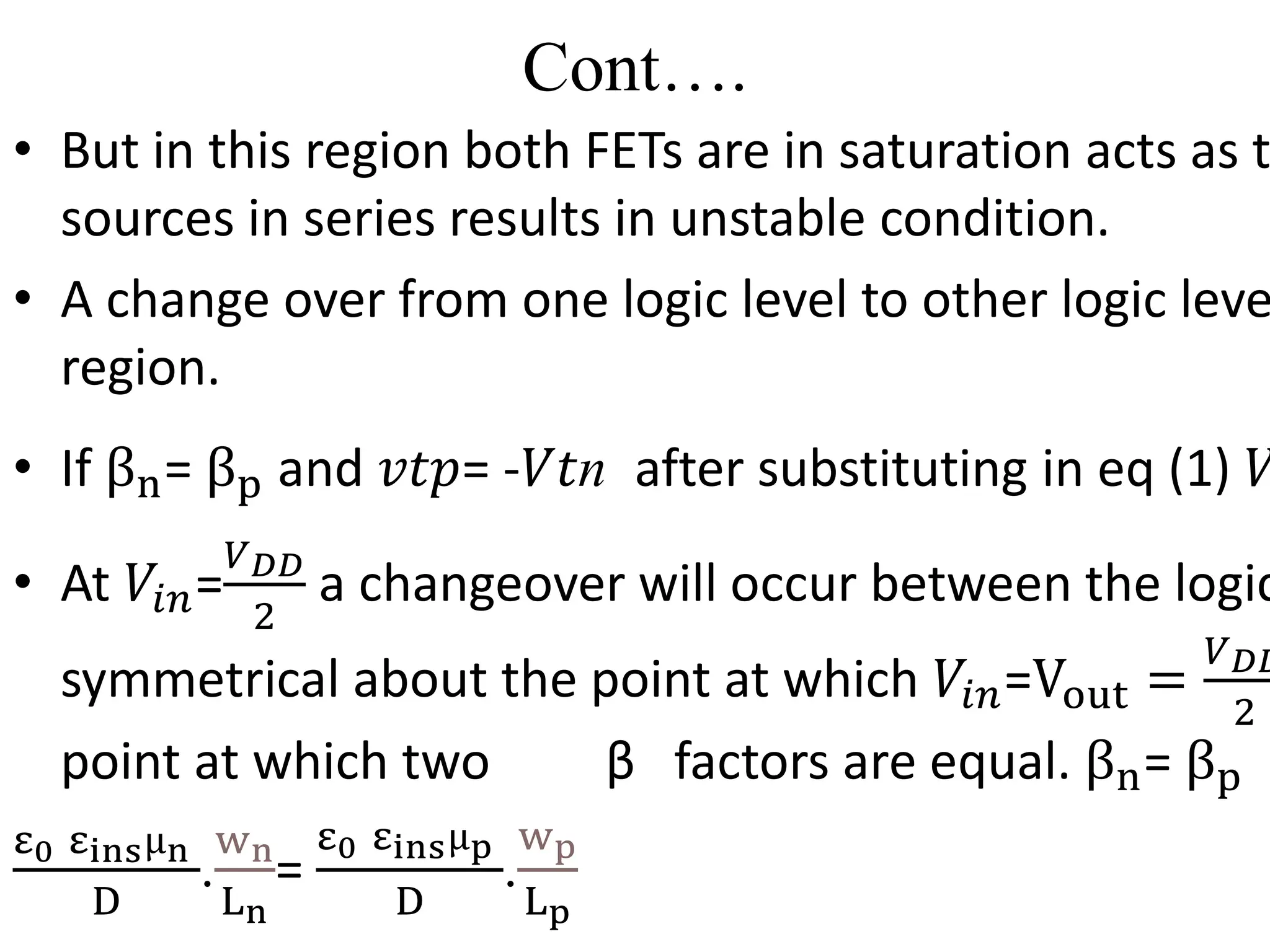
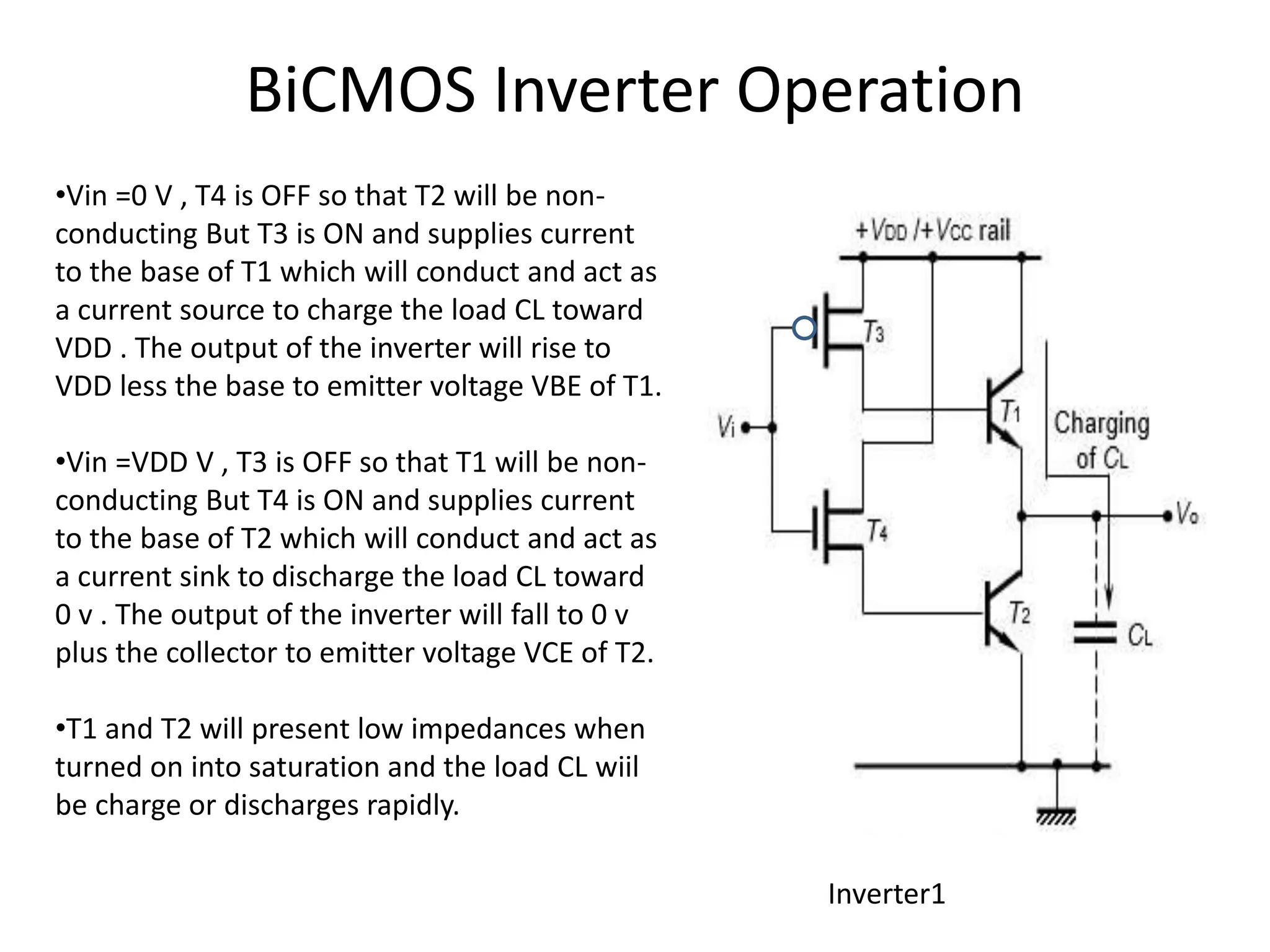
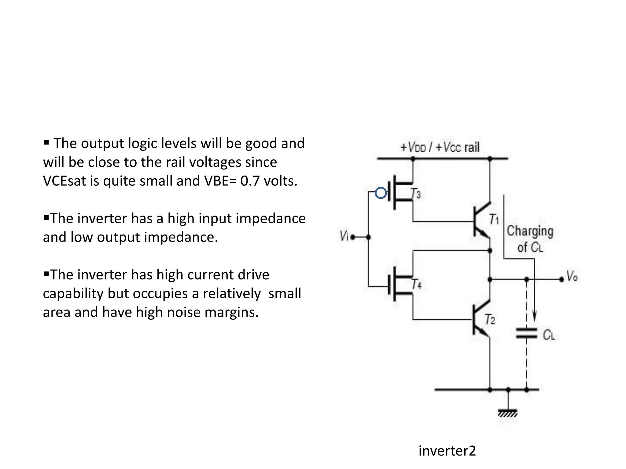
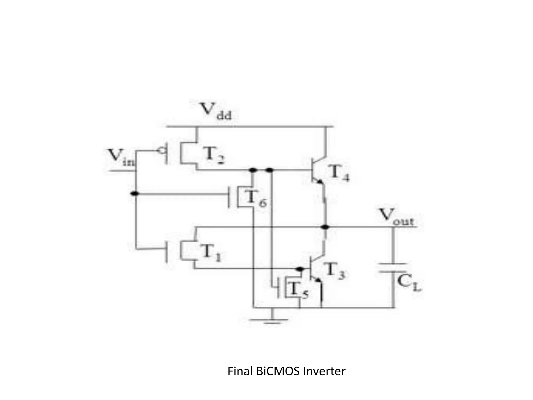
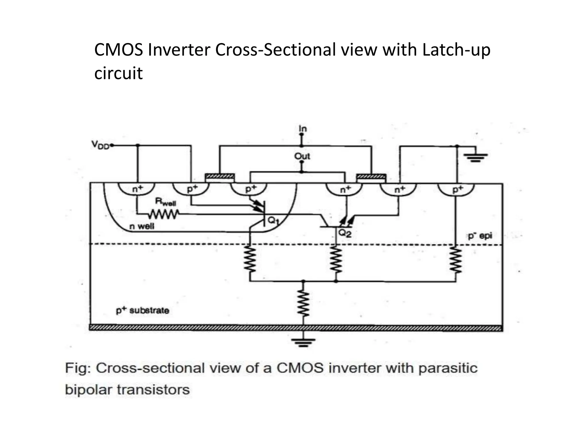
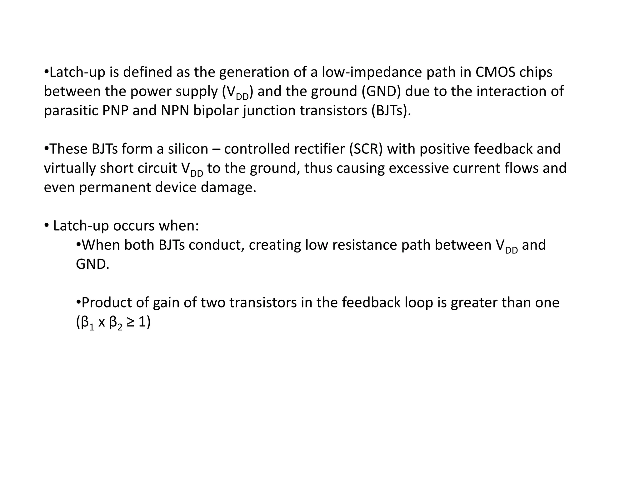
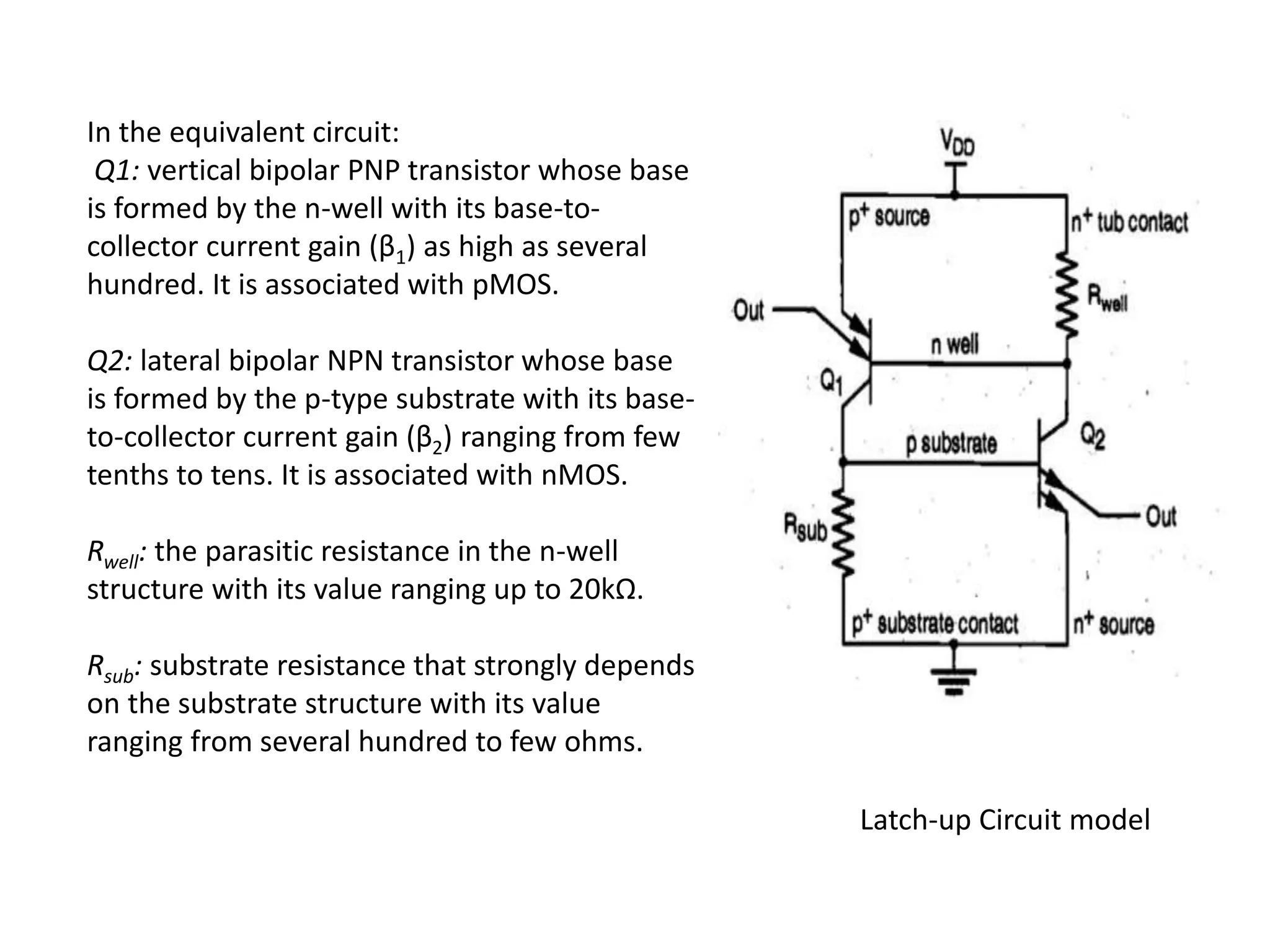
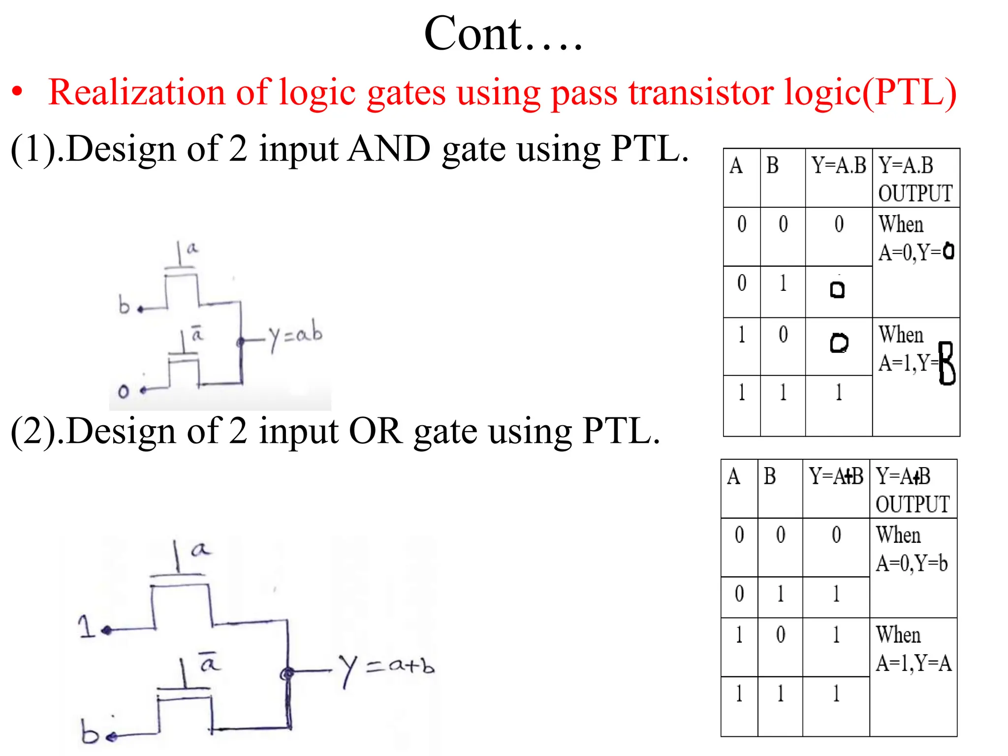
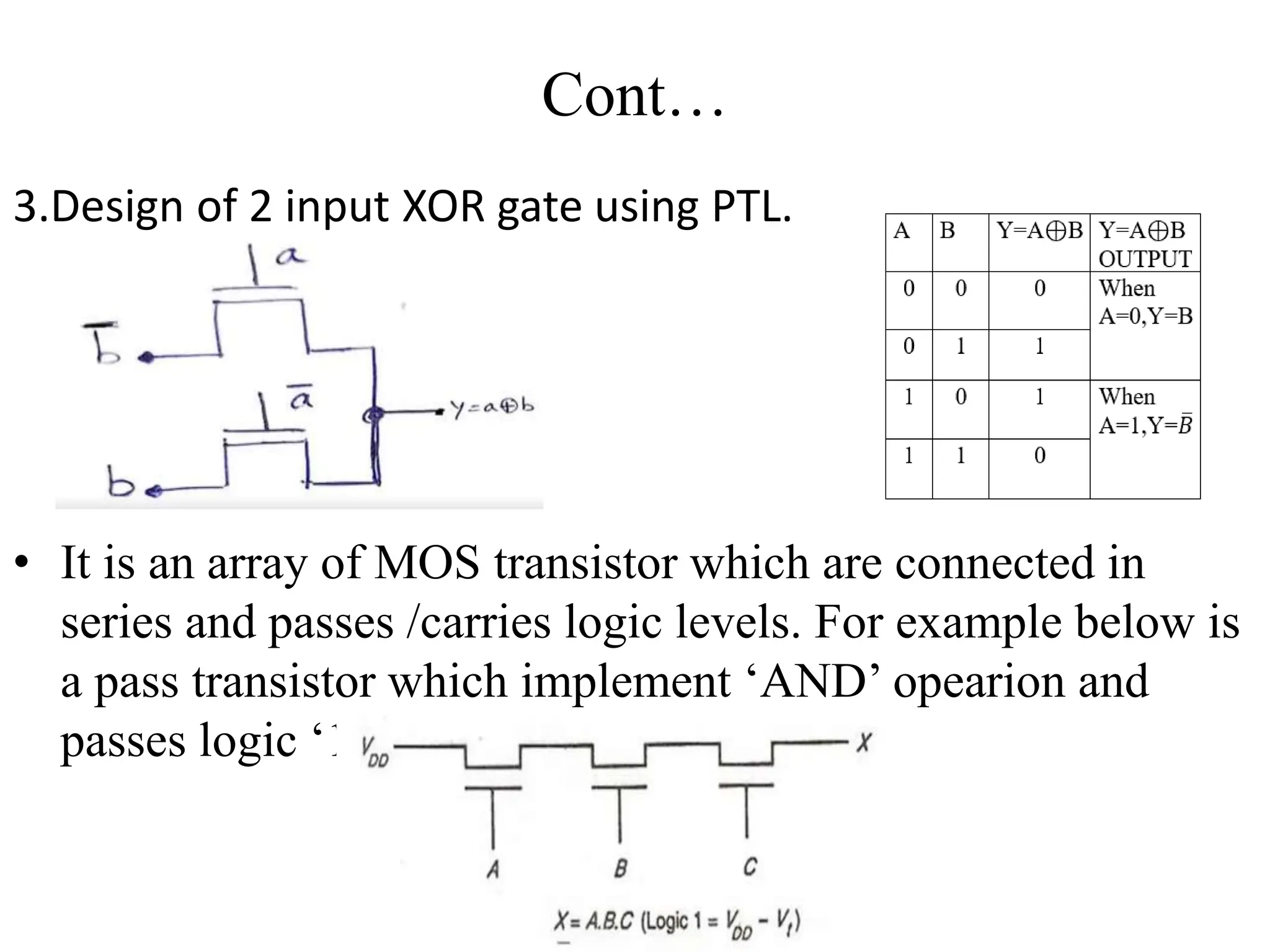
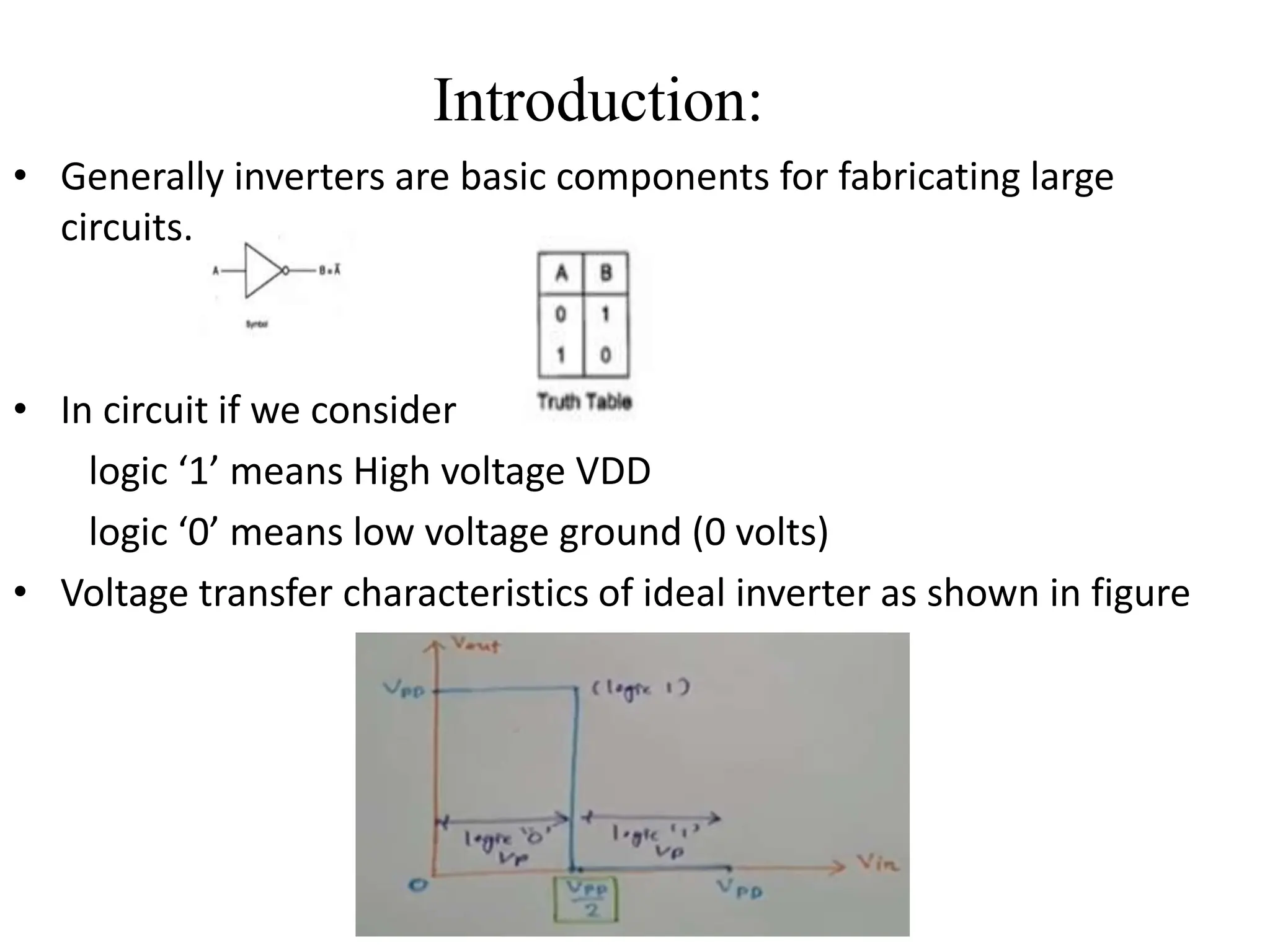
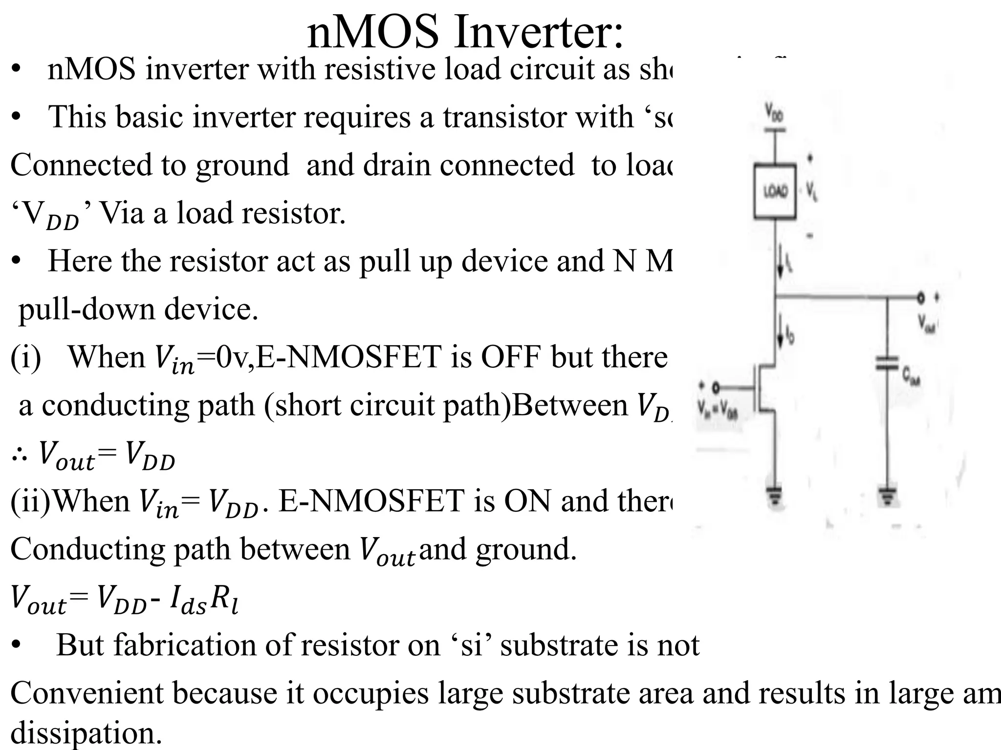
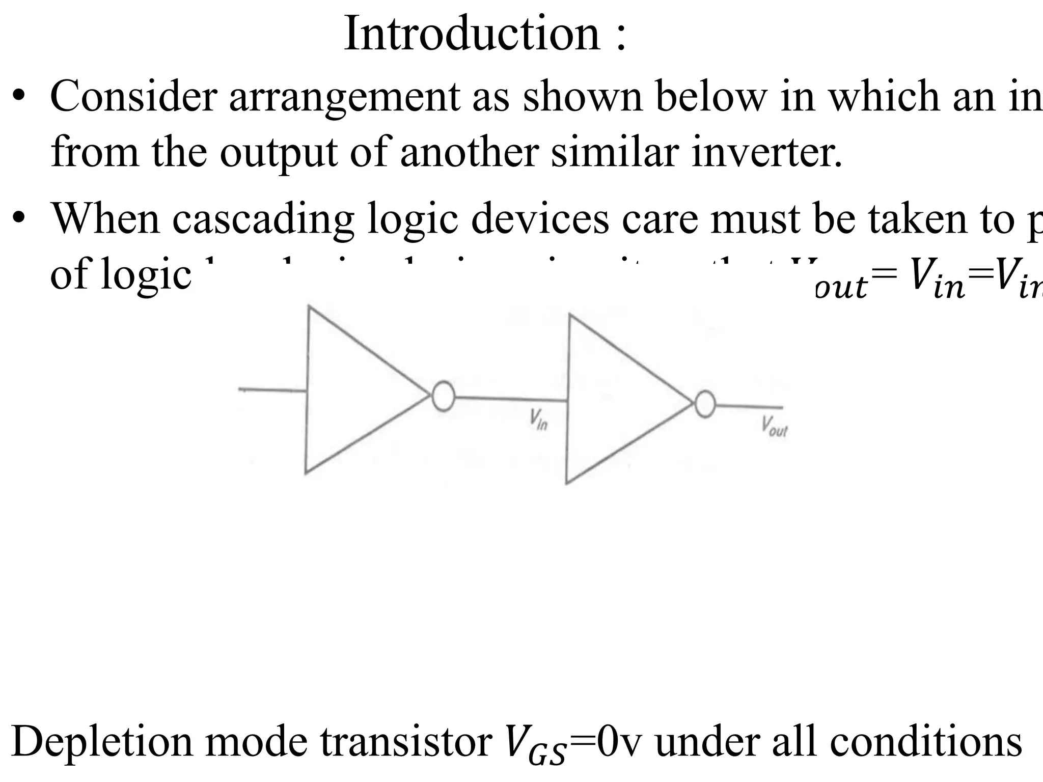
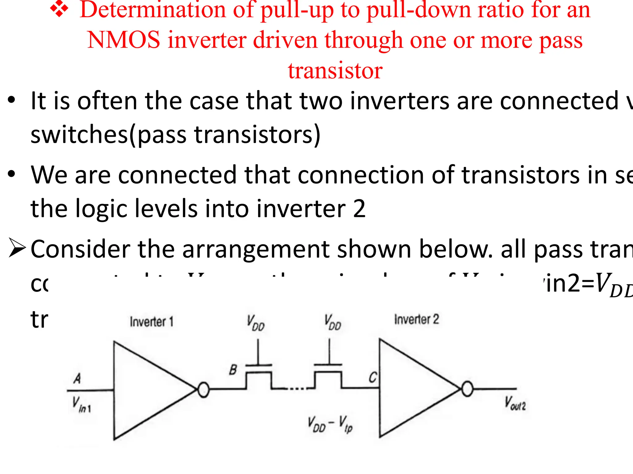
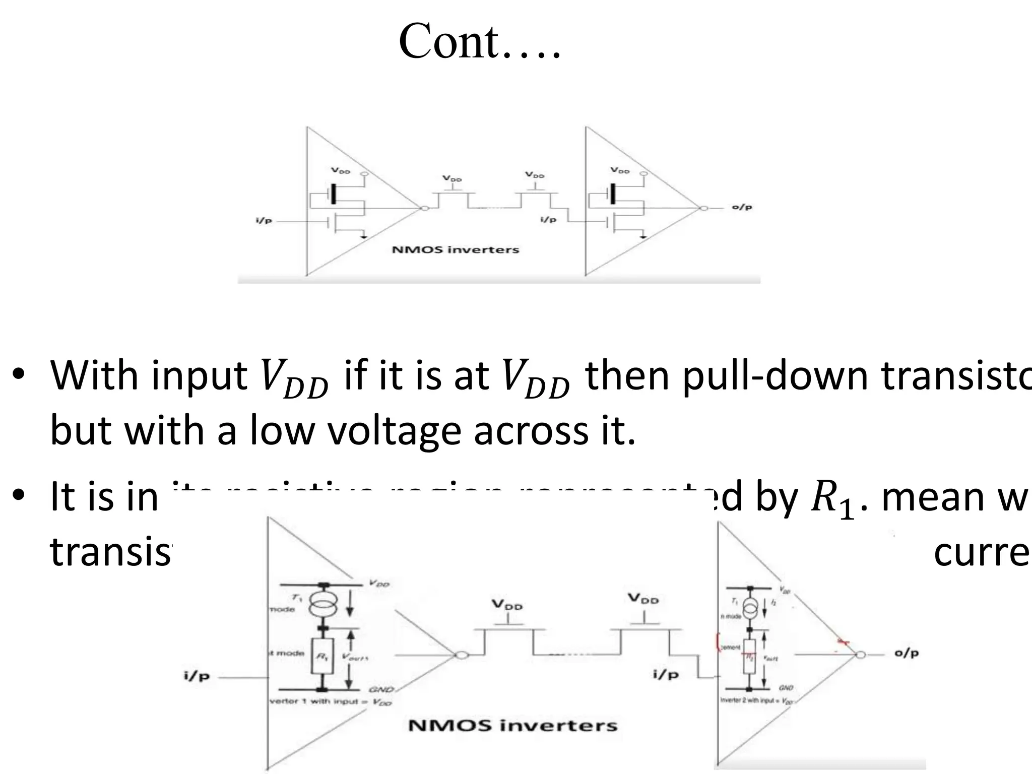
The document provides an overview of pass transistor concepts, discussing how nMOS and pMOS transistors function as switches, details on designing logic gates with pass transistors, and the characteristics of inverters using nMOS and CMOS technology. Additionally, it describes the challenges of latch-up in CMOS circuits, outlining the conditions that lead to low-impedance paths between power and ground resulting in excessive current flows. Various technical parameters and operational conditions are analyzed to ensure proper functioning and minimize issues in transistor designs.


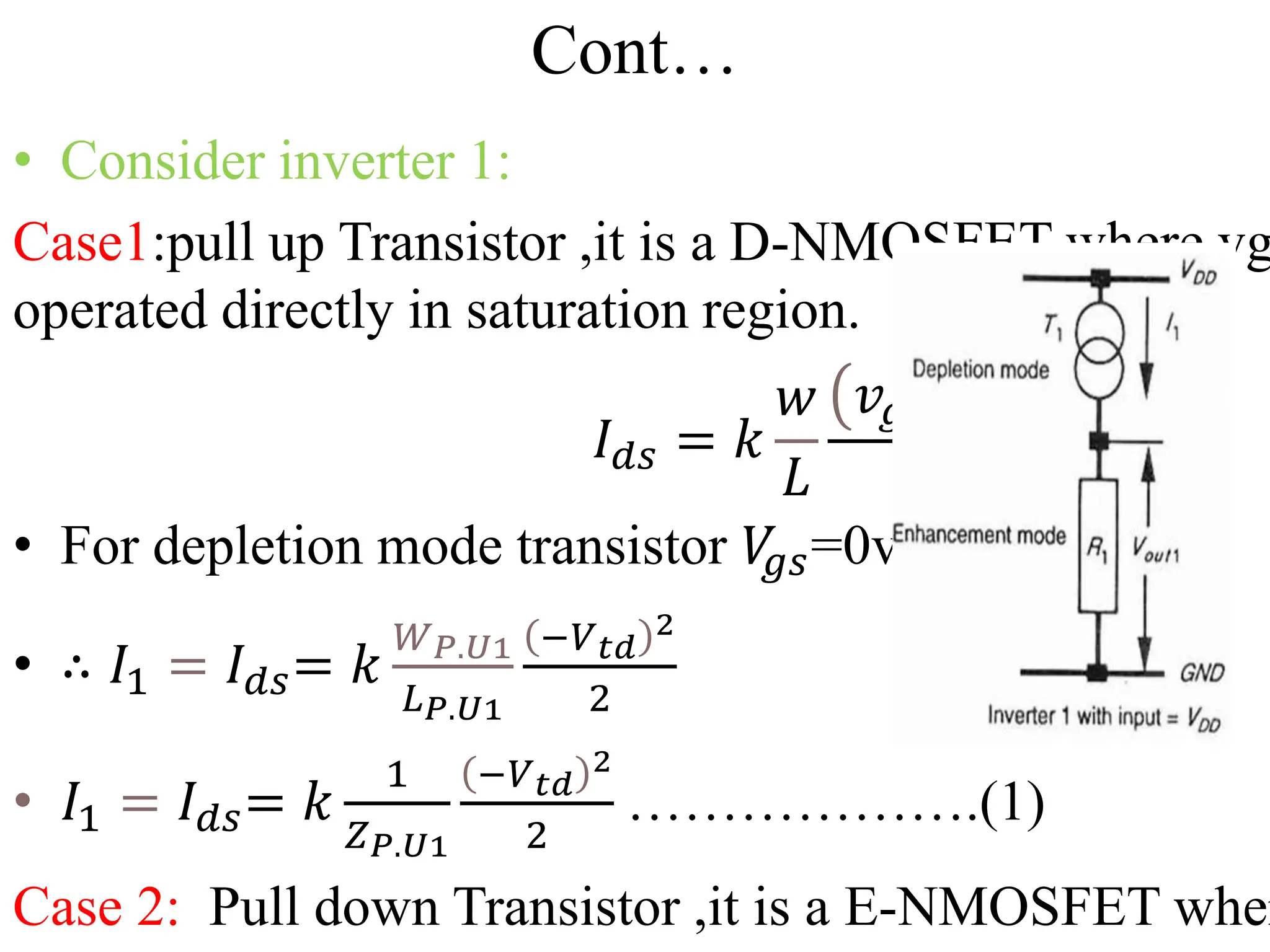
![Cont….
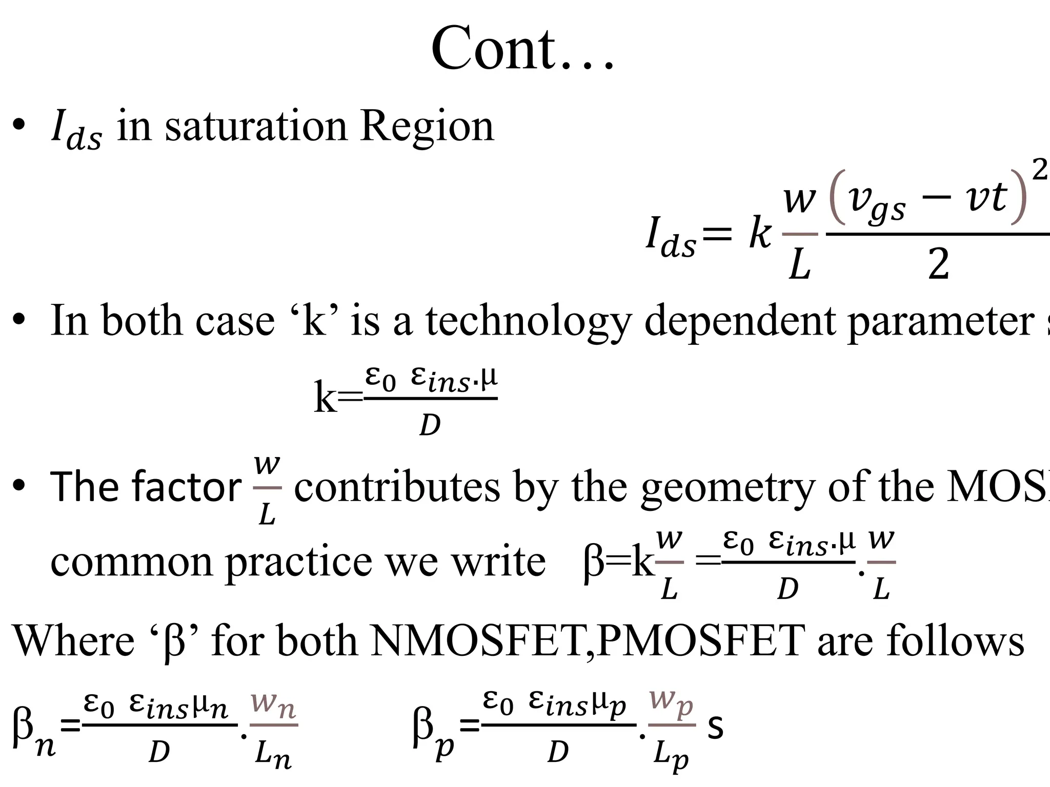
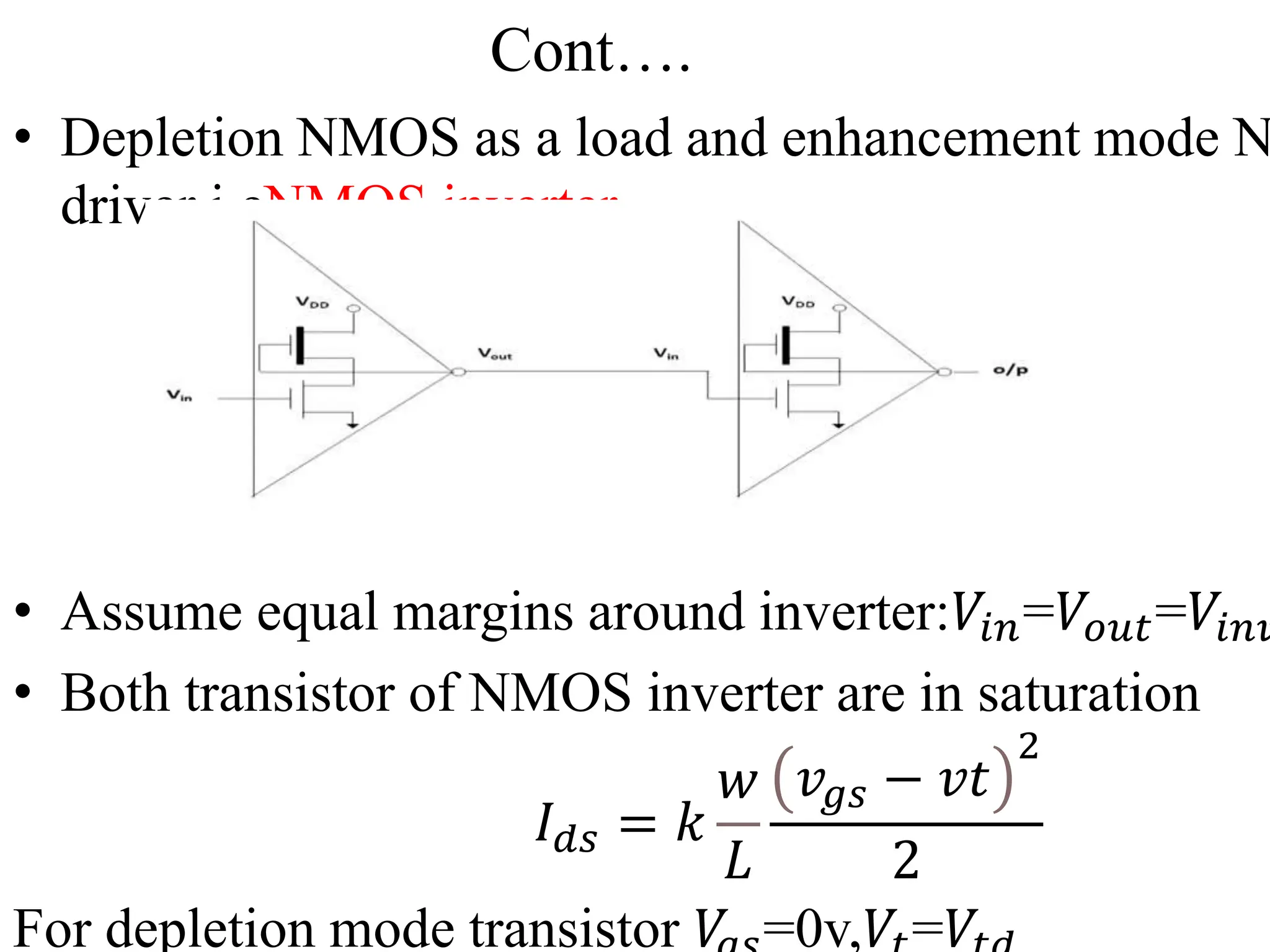
• ∴ 𝐼𝑑𝑠 = 𝑘
𝑊𝑃.𝑈
𝐿𝑃.𝑈
−𝑉𝑡𝑑
2
2
……………….(1)
• For enhancement mode transistor 𝑉
𝑔𝑠=𝑉𝑖𝑛𝑣
∴ 𝐼𝑑𝑠 = 𝑘
𝑊𝑃.𝑑
𝐿𝑃.𝑑
𝑉𝑖𝑛𝑣 −𝑣𝑡 2
2
……..(2)
Since currents are equal then
𝑘
𝑊𝑃.𝑈
𝐿𝑃.𝑈
−𝑉𝑡𝑑
2
2
= 𝑘
𝑊𝑃.𝑑
𝐿𝑃.𝑑
𝑉𝑖𝑛𝑣 −𝑣𝑡 2
2
[convention Z=
𝐿
𝑊
]
1
𝑧𝑃.𝑈
.
−𝑉𝑡𝑑
2
2
=
1
𝑧𝑃.𝐷
.
𝑉𝑖𝑛𝑣 −𝑣𝑡 2
2
𝑉𝑡𝑑](https://image.slidesharecdn.com/transistorlogic-240614112602-9a9b6afb/75/Transistor-logic-of-vlsi-subject-for-ece-pptx-17-2048.jpg)
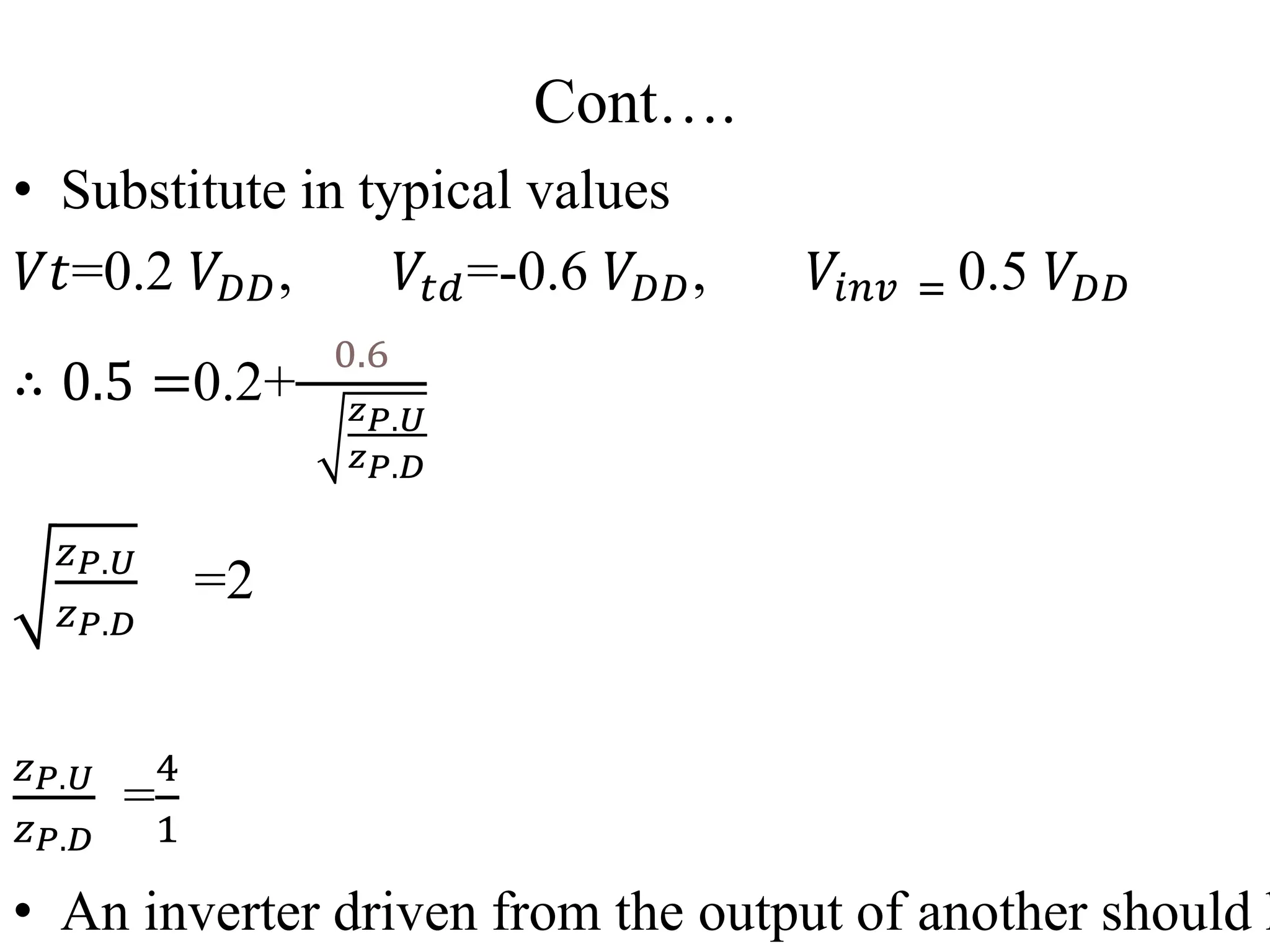
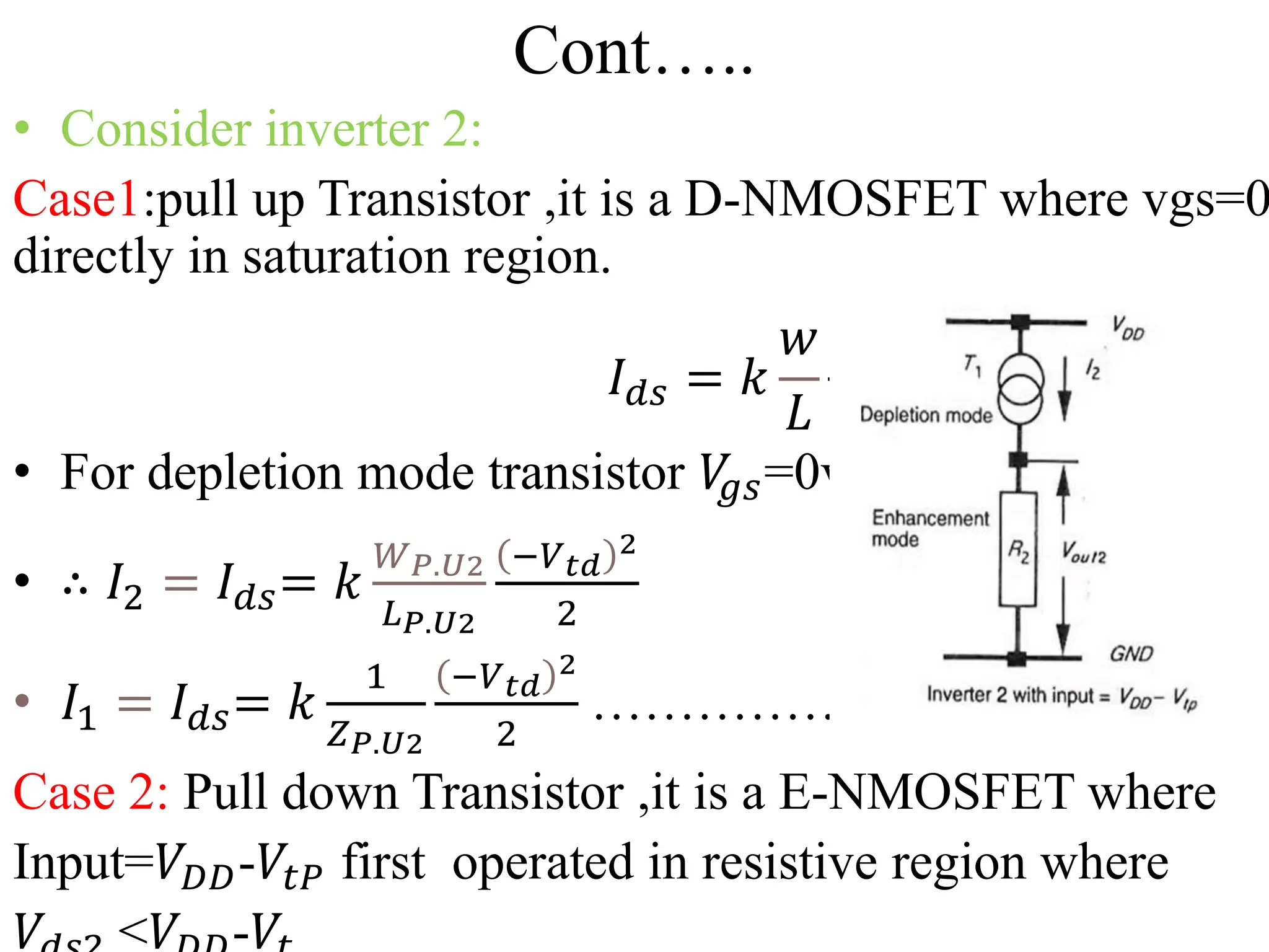
![Cont…
• ∴ 𝐼𝑑𝑠 = 𝐼1= 𝑘
𝑊𝑃.𝑑1
𝐿𝑃.𝑑1
[(𝑉𝐷𝐷-𝑉𝑡 )𝑉𝑑𝑠1 -
𝑉𝑑𝑠1
2
2
]
𝑅1 =
𝑉𝑑𝑠1
𝐼1
=
1
𝑘
𝑍𝑃.𝐷1
1
[(𝑉𝐷𝐷 −𝑉𝑡 ) −𝑉𝑑𝑠1
2
]
Note:𝑉𝑑𝑠1 is small so ignore
𝑉𝑑𝑠1
2
𝑅1 =
𝑉𝑑𝑠1
𝐼1
=
1
𝑘
𝑍𝑃.𝐷1
1
[(𝑉𝐷𝐷 −𝑉𝑡 )]
…….(2)
• The output of the inverter 1 i.e equations (1) and (2) s
equation
𝑉𝑜𝑢𝑡1=𝐼1.𝑅1=𝑘
1
𝑍𝑃.𝑈1
−𝑉𝑡𝑑
2
2
.
1
𝑘
𝑍𝑃.𝐷1
1
[(𝑉𝐷𝐷 −𝑉𝑡 )]](https://image.slidesharecdn.com/transistorlogic-240614112602-9a9b6afb/75/Transistor-logic-of-vlsi-subject-for-ece-pptx-23-2048.jpg)
![Cont…
• 𝐼𝑑𝑠 = 𝐼1= 𝑘
𝑊𝑃.𝑑2
𝐿𝑃.𝑑2
[(𝑉𝐷𝐷-𝑉𝑡 )𝑉𝑑𝑠1 -
𝑉𝑑𝑠1
2
2
]
• But 𝑉𝐷𝐷 =𝑉𝐷𝐷-𝑉𝑡𝑃
• 𝐼𝑑𝑠 = 𝐼1= 𝑘
𝑊𝑃.𝑑2
𝐿𝑃.𝑑2
[(𝑉𝐷𝐷-𝑉𝑡𝑃-𝑉𝑡 )𝑉𝑑𝑠2 -
𝑉𝑑𝑠2
2
2
]
𝑅2 =
𝑉𝑑𝑠2
𝐼2
=
1
𝑘
𝑍𝑃.𝐷2
1
[(𝑉𝐷𝐷− 𝑉𝑡𝑃−𝑉𝑡 ) −𝑉𝑑𝑠2
2
]
Note:𝑉𝑑𝑠2 is small so ignore
𝑉𝑑𝑠2
2
• 𝑅1 =
𝑉𝑑𝑠1
𝐼1
=
1
𝑘
𝑍𝑃.𝐷1
1
[(𝑉𝐷𝐷− 𝑉𝑡𝑃−𝑉𝑡 )]
…….(5)
• The output of the inverter 1 i.e equations (4) and (5) s
equation](https://image.slidesharecdn.com/transistorlogic-240614112602-9a9b6afb/75/Transistor-logic-of-vlsi-subject-for-ece-pptx-25-2048.jpg)
![Cont…
• 𝑉𝑜𝑢𝑡2=𝐼2.𝑅2=
𝑍𝑃.𝐷2
𝑍𝑃.𝑈2
.
1
[(𝑉𝐷𝐷− 𝑉𝑡𝑃−𝑉𝑡 )]
.
−𝑉𝑡𝑑
2
2
……(6)
• 𝑉𝑜𝑢𝑡1 = 𝑉𝑜𝑢𝑡2
•
𝑍𝑃.𝐷1
𝑍𝑃.𝑈1
.
1
[(𝑉𝐷𝐷 −𝑉𝑡 )]
.
−𝑉𝑡𝑑
2
2
=
𝑍𝑃.𝐷1
𝑍𝑃.𝑈2
.
1
[(𝑉𝐷𝐷− 𝑉𝑡𝑃−𝑉𝑡 )]
.
−𝑉𝑡𝑑
2
2
𝑍𝑃.𝑈1
𝑍𝑃.𝐷1
(𝑉𝐷𝐷 −𝑉𝑡 )=
𝑍𝑃.𝑈2
𝑍𝑃.𝐷2
(𝑉𝐷𝐷− 𝑉𝑡𝑃−𝑉𝑡 )
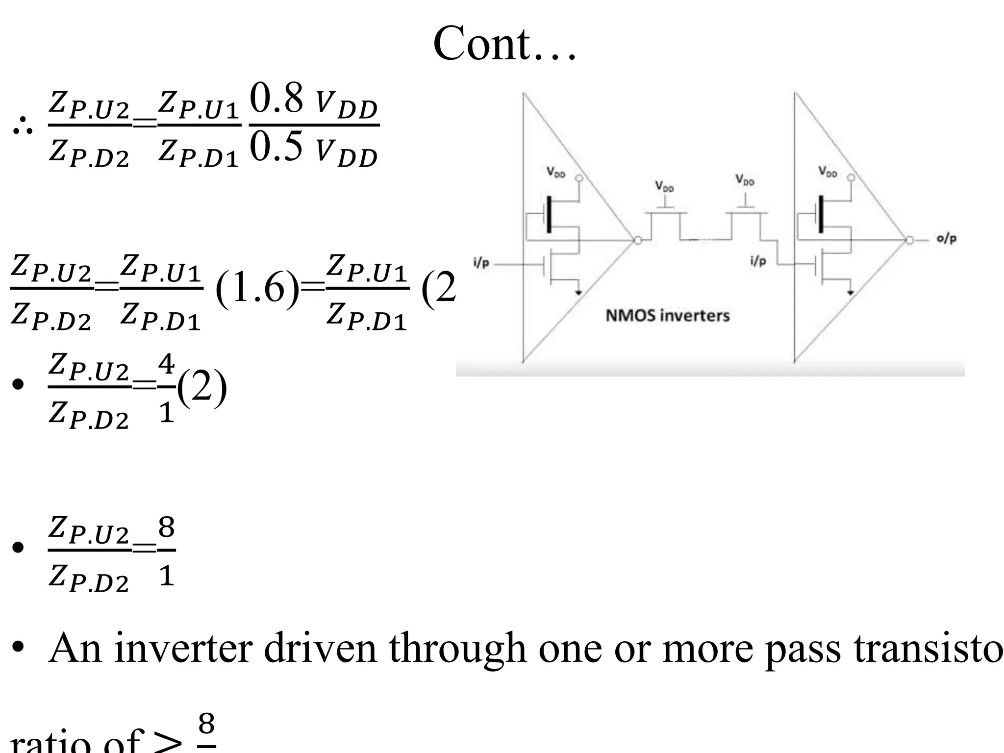
• Typical values 𝑉𝑡 =0.2𝑉𝐷𝐷 and 𝑉𝑡𝑃= 0.3𝑉𝐷𝐷
•
𝑍𝑃.𝑈1
𝑍𝑃.𝐷1
(𝑉𝐷𝐷 −0.2 𝑉𝐷𝐷)=
𝑍𝑃.𝑈2
𝑍𝑃.𝐷2
(𝑉𝐷𝐷−0.3 𝑉𝐷𝐷−0.2 𝑉𝐷𝐷)
𝑍𝑃.𝑈1
𝑍𝑃.𝐷1
(0.8 𝑉𝐷𝐷)=
𝑍𝑃.𝑈2
𝑍𝑃.𝐷2
(0.5 𝑉𝐷𝐷)](https://image.slidesharecdn.com/transistorlogic-240614112602-9a9b6afb/75/Transistor-logic-of-vlsi-subject-for-ece-pptx-26-2048.jpg)