This document provides lecture notes on MOS design equations and parameters. It includes:
- MOS transistor symbol definitions and varieties
- Support equations for threshold voltage, subthreshold slope, gate overdrive voltage, velocity saturation, drain current factor, channel length modulation, and thermal voltage
- Current equations for strong, weak, and moderate inversion regions
- Sample MOSFET parameters for 0.35μm and 0.18μm processes
- Problems involving calculating small signal parameters, voltage gain, and transistor sizing for different circuits like common source amplifiers, NAND gates, and current mirrors.
Original N-Channel Power MOSFET IRF1010EPBF IRF1010 1010 60V 84A TO-220 New I...AUTHELECTRONIC
Original N-Channel Power MOSFET IRF1010EPBF IRF1010 1010 60V 84A TO-220 New International Rectifier
https://authelectronic.com/original-n-channel-power-mosfet-irf1010epbf-irf1010-1010-60v-84a-to-220-new-international-rectifier
IJERA (International journal of Engineering Research and Applications) is International online, ... peer reviewed journal. For more detail or submit your article, please visit www.ijera.com
pull up to pull down ratio of nmos inverter driven by another nmos inverter and also another describing with pass transistor. Transistor sizing with example and some formulas
Dee 6113 CMOS IC DESIGN (Chapter 3 ~ CMOS inverter)MielWitwicky
Question 4
a) Draw a schematic diagram of an inverter.
b) Voltage Transfer Characteristics (VTC) is a plot of output voltage as a function of the input voltage. Draw and label the VTC of a CMOS inverter.
c) The inverter is really the nucleus of all digital design. Once its operation and properties are clearly understood, designing more intricate structures such as NAND gates, address, multipliers, and microprocessors is greatly simplified. Therefore, interpret the properties of static CMOS inverter circuit.
Original N-Channel Mosfet IRFI4019H-117P 4019 8A 150V TO-220 NewAUTHELECTRONIC
Original N-Channel Mosfet IRFI4019H-117P 4019 8A 150V TO-220 New
https://authelectronic.com/original-n-channel-mosfet-irfi4019h-117p-4019-8a-150v-to-220-new
Original N-Channel Mosfet IRFI4019H-117P 4019 8A 150V TO-220 NewAUTHELECTRONIC
Original N-Channel Mosfet IRFI4019H-117P 4019 8A 150V TO-220 New
https://authelectronic.com/original-n-channel-mosfet-irfi4019h-117p-4019-8a-150v-to-220-new
Original P Channel Mosfet IRF9Z34 IRF9Z34N IRF9Z34NPBF 9Z34 60V 18A TO 220 NewAUTHELECTRONIC
Original P Channel Mosfet IRF9Z34 IRF9Z34N IRF9Z34NPBF 9Z34 60V 18A TO 220 New
https://authelectronic.com/original-p-channel-mosfet-irf9z34-irf9z34n-irf9z34npbf-9z34-60v-18a-to-220-new
Gene's law, Common gate, kernel Principal Component Analysis, ASIC Physical Design Post-Layout Verification, TSMC180nm, 0.13um IBM CMOS technology, Cadence Virtuoso, FPAA, in Spanish, Bruun E,
Lab 2: Cadence Tutorial on Layout and DRC/LVS/PEX
This section describes how to extract a netlist from your layout that includes parasitic resistances and capacitances. You will then be able to re-simulate your design with extracted parasitics in Spectre. PEX requires a clean LVS so that extracted parasitics can be correlated to nets on the schematic. Initiate the PEX interface by clicking on:Calibre > Run PEX
A window asking to load a runset file will now appear. Browse to the file
Step by step process of uploading presentation videos Hoopeer Hoopeer
Deep neural network, compressive sensing, floating gate techniques can be efficiently employed to increase voltage swing and reduce supply voltage requirements of class AB regulated cascode current mirrors, implement extreme low power analog circuits with this process. /also have good references for subthreshold region.
[Extreme Low Power Differential Pair: An Experimental Evaluation, Super-Gain-Boosted Miller Op-Amp based on Nested Regulated Cascode Techniques , Step by Step process of uploading presentation videos, Dennis Ritchie The creator of the C programming language and co-creator of Unix
Influential and powerful professional electrical and electronics engineering ...Hoopeer Hoopeer
powerful professional electrical and electronics engineering books
. Analysis and Design of Analog Integrated Circuits
Analysis and Design of Analog Integrated Circuits
Analog filter design
BJT and MOS, Advanced Circuit Topologies, concept of tracking, mm-Wave frequency beyond 30GHz, Bandgap is a stable, well defined, and constant current source
About
Indigenized remote control interface card suitable for MAFI system CCR equipment. Compatible for IDM8000 CCR. Backplane mounted serial and TCP/Ethernet communication module for CCR remote access. IDM 8000 CCR remote control on serial and TCP protocol.
• Remote control: Parallel or serial interface.
• Compatible with MAFI CCR system.
• Compatible with IDM8000 CCR.
• Compatible with Backplane mount serial communication.
• Compatible with commercial and Defence aviation CCR system.
• Remote control system for accessing CCR and allied system over serial or TCP.
• Indigenized local Support/presence in India.
• Easy in configuration using DIP switches.
Technical Specifications
Indigenized remote control interface card suitable for MAFI system CCR equipment. Compatible for IDM8000 CCR. Backplane mounted serial and TCP/Ethernet communication module for CCR remote access. IDM 8000 CCR remote control on serial and TCP protocol.
Key Features
Indigenized remote control interface card suitable for MAFI system CCR equipment. Compatible for IDM8000 CCR. Backplane mounted serial and TCP/Ethernet communication module for CCR remote access. IDM 8000 CCR remote control on serial and TCP protocol.
• Remote control: Parallel or serial interface
• Compatible with MAFI CCR system
• Copatiable with IDM8000 CCR
• Compatible with Backplane mount serial communication.
• Compatible with commercial and Defence aviation CCR system.
• Remote control system for accessing CCR and allied system over serial or TCP.
• Indigenized local Support/presence in India.
Application
• Remote control: Parallel or serial interface.
• Compatible with MAFI CCR system.
• Compatible with IDM8000 CCR.
• Compatible with Backplane mount serial communication.
• Compatible with commercial and Defence aviation CCR system.
• Remote control system for accessing CCR and allied system over serial or TCP.
• Indigenized local Support/presence in India.
• Easy in configuration using DIP switches.
Welcome to WIPAC Monthly the magazine brought to you by the LinkedIn Group Water Industry Process Automation & Control.
In this month's edition, along with this month's industry news to celebrate the 13 years since the group was created we have articles including
A case study of the used of Advanced Process Control at the Wastewater Treatment works at Lleida in Spain
A look back on an article on smart wastewater networks in order to see how the industry has measured up in the interim around the adoption of Digital Transformation in the Water Industry.
Automobile Management System Project Report.pdfKamal Acharya
The proposed project is developed to manage the automobile in the automobile dealer company. The main module in this project is login, automobile management, customer management, sales, complaints and reports. The first module is the login. The automobile showroom owner should login to the project for usage. The username and password are verified and if it is correct, next form opens. If the username and password are not correct, it shows the error message.
When a customer search for a automobile, if the automobile is available, they will be taken to a page that shows the details of the automobile including automobile name, automobile ID, quantity, price etc. “Automobile Management System” is useful for maintaining automobiles, customers effectively and hence helps for establishing good relation between customer and automobile organization. It contains various customized modules for effectively maintaining automobiles and stock information accurately and safely.
When the automobile is sold to the customer, stock will be reduced automatically. When a new purchase is made, stock will be increased automatically. While selecting automobiles for sale, the proposed software will automatically check for total number of available stock of that particular item, if the total stock of that particular item is less than 5, software will notify the user to purchase the particular item.
Also when the user tries to sale items which are not in stock, the system will prompt the user that the stock is not enough. Customers of this system can search for a automobile; can purchase a automobile easily by selecting fast. On the other hand the stock of automobiles can be maintained perfectly by the automobile shop manager overcoming the drawbacks of existing system.
Water scarcity is the lack of fresh water resources to meet the standard water demand. There are two type of water scarcity. One is physical. The other is economic water scarcity.
Event Management System Vb Net Project Report.pdfKamal Acharya
In present era, the scopes of information technology growing with a very fast .We do not see any are untouched from this industry. The scope of information technology has become wider includes: Business and industry. Household Business, Communication, Education, Entertainment, Science, Medicine, Engineering, Distance Learning, Weather Forecasting. Carrier Searching and so on.
My project named “Event Management System” is software that store and maintained all events coordinated in college. It also helpful to print related reports. My project will help to record the events coordinated by faculties with their Name, Event subject, date & details in an efficient & effective ways.
In my system we have to make a system by which a user can record all events coordinated by a particular faculty. In our proposed system some more featured are added which differs it from the existing system such as security.
Forklift Classes Overview by Intella PartsIntella Parts
Discover the different forklift classes and their specific applications. Learn how to choose the right forklift for your needs to ensure safety, efficiency, and compliance in your operations.
For more technical information, visit our website https://intellaparts.com
Cosmetic shop management system project report.pdfKamal Acharya
Buying new cosmetic products is difficult. It can even be scary for those who have sensitive skin and are prone to skin trouble. The information needed to alleviate this problem is on the back of each product, but it's thought to interpret those ingredient lists unless you have a background in chemistry.
Instead of buying and hoping for the best, we can use data science to help us predict which products may be good fits for us. It includes various function programs to do the above mentioned tasks.
Data file handling has been effectively used in the program.
The automated cosmetic shop management system should deal with the automation of general workflow and administration process of the shop. The main processes of the system focus on customer's request where the system is able to search the most appropriate products and deliver it to the customers. It should help the employees to quickly identify the list of cosmetic product that have reached the minimum quantity and also keep a track of expired date for each cosmetic product. It should help the employees to find the rack number in which the product is placed.It is also Faster and more efficient way.
Explore the innovative world of trenchless pipe repair with our comprehensive guide, "The Benefits and Techniques of Trenchless Pipe Repair." This document delves into the modern methods of repairing underground pipes without the need for extensive excavation, highlighting the numerous advantages and the latest techniques used in the industry.
Learn about the cost savings, reduced environmental impact, and minimal disruption associated with trenchless technology. Discover detailed explanations of popular techniques such as pipe bursting, cured-in-place pipe (CIPP) lining, and directional drilling. Understand how these methods can be applied to various types of infrastructure, from residential plumbing to large-scale municipal systems.
Ideal for homeowners, contractors, engineers, and anyone interested in modern plumbing solutions, this guide provides valuable insights into why trenchless pipe repair is becoming the preferred choice for pipe rehabilitation. Stay informed about the latest advancements and best practices in the field.
Sachpazis:Terzaghi Bearing Capacity Estimation in simple terms with Calculati...Dr.Costas Sachpazis
Terzaghi's soil bearing capacity theory, developed by Karl Terzaghi, is a fundamental principle in geotechnical engineering used to determine the bearing capacity of shallow foundations. This theory provides a method to calculate the ultimate bearing capacity of soil, which is the maximum load per unit area that the soil can support without undergoing shear failure. The Calculation HTML Code included.
COLLEGE BUS MANAGEMENT SYSTEM PROJECT REPORT.pdfKamal Acharya
The College Bus Management system is completely developed by Visual Basic .NET Version. The application is connect with most secured database language MS SQL Server. The application is develop by using best combination of front-end and back-end languages. The application is totally design like flat user interface. This flat user interface is more attractive user interface in 2017. The application is gives more important to the system functionality. The application is to manage the student’s details, driver’s details, bus details, bus route details, bus fees details and more. The application has only one unit for admin. The admin can manage the entire application. The admin can login into the application by using username and password of the admin. The application is develop for big and small colleges. It is more user friendly for non-computer person. Even they can easily learn how to manage the application within hours. The application is more secure by the admin. The system will give an effective output for the VB.Net and SQL Server given as input to the system. The compiled java program given as input to the system, after scanning the program will generate different reports. The application generates the report for users. The admin can view and download the report of the data. The application deliver the excel format reports. Because, excel formatted reports is very easy to understand the income and expense of the college bus. This application is mainly develop for windows operating system users. In 2017, 73% of people enterprises are using windows operating system. So the application will easily install for all the windows operating system users. The application-developed size is very low. The application consumes very low space in disk. Therefore, the user can allocate very minimum local disk space for this application.
Quality defects in TMT Bars, Possible causes and Potential Solutions.PrashantGoswami42
Maintaining high-quality standards in the production of TMT bars is crucial for ensuring structural integrity in construction. Addressing common defects through careful monitoring, standardized processes, and advanced technology can significantly improve the quality of TMT bars. Continuous training and adherence to quality control measures will also play a pivotal role in minimizing these defects.
Quality defects in TMT Bars, Possible causes and Potential Solutions.
Tluenotes lehmann
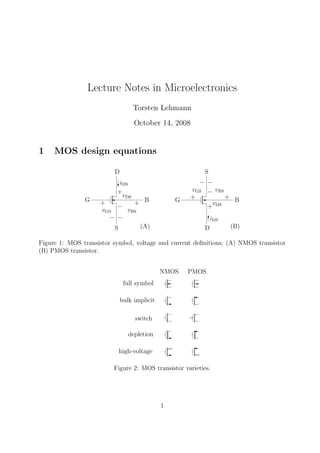
1. Lecture Notes in Microelectronics
Torsten Lehmann
October 14, 2008
1 MOS design equations
S
B
D
G
−
+
D
B
S
G +
vGS
−
+
−
vBS
vDS
+
−
+
−
vGS
iDS
vDS
+
iDS
−
vBS
(B)(A)
Figure 1: MOS transistor symbol, voltage and current definitions; (A) NMOS transistor
(B) PMOS transistor.
NMOS PMOS
full symbol
bulk implicit
switch
depletion
high-voltage
Figure 2: MOS transistor varieties.
1
2. 1.1 Support equations
threshold voltage Vth = Vth0 + γ |2φF − vBS| − |2φF| (1)
n/p sign function |x|p ≡
x for n-channel
−x for p-channel
; |x|p =
γ
|γ|
x (2)
sub-threshold slope n =
γ
2 |2φF − vBS|
+ |1|p (3)
gate-overdrive voltage vEff = vGS − Vth (4)
velocity saturation µ =
µ0
1 + vDS/(ECritL)
(5)
drain saturation voltage vDSsat = LECrit 1 + 2vEff/(LECrit) − 1 (6)
≃ vEff, |2vEff|p ≪ |LECrit|p (7)
drain current factor β =
W
L
K′
=
W
L
µCox; K′
= µCox (8)
channel-length modulation α = 1 + λvDS = 1 +
kλvDS
L
; λ =
kλ
L
(9)
thermal voltage VT = kT/q (10)
sub-threshold scale current I0 = 1
2
µCox(2nVT )2
(11)
weak-strong transition IWST = I0 ln2
(2)
W
L
(12)
1.2 Current equations
Strong inversion (|vEff|p >∼ |2nVT ln(10)|p, or |IDS,sat|p ≫ |IWST|p):
iDS = µCox
W
L
vEffvDS − 1
2
v2
DS α, |vDSsat|p > |vDS|p (triode) (13)
iDS = IDS,sat = µCox
W
L
vEffvDSsat − 1
2
v2
DSsat α, |vDSsat|p ≤ |vDS|p (saturation)(14)
≃ 1
2
µCox
W
L
v2
Effα, |2vEff|p ≪ |LECrit|p (not velocity saturated) (15)
≃ µ0CoxECritW vEff − 1
2
vDSsat α, |2vEff|p ≫ |LECrit|p (deep velocity sat.) (16)
Weak inversion (|vEff|p <∼ −|2nVT ln(10)|p, or |IDS,sat|p ≪ |IWST|p):
iDS = I0
W
L
evEff /(nVT )
1 − e−|vDS|p/VT
α (17)
iDS = IDS,sat = I0
W
L
evEff /(nVT )
α, |nVT |p ≪ |vDS|p (saturation) (18)
Moderate inversion saturation (|vDS|p ≫ |nVT |p, and |vDS|p > |vEff|p):
iDS = IDS,sat = 1
2
µCox
W
L
(2nVT )2
ln2
1 + evEff /(2nVT )
α (19)
2
3. 0.001
0.01
0.1
1
10
100
1000
-4 -2 0 2 4
iDS/Iwst
veff/nVT
current expression
(log(1+exp(x/2))/log(2))**2
x**2/(log(2)*2)**2
exp(x)/log(2)**2
Figure 3: Normalised saturation current
1.3 Sample MOST parameters
Typical parameters for some CMOS processes (preliminary):
Process 0.35 µm 0.18 µm
Parameter n-channel p-channel n-channel p-channel
VDD,max 2.5 V 2.5 V 1.8 V 1.8 V
Vth0 0.6 V −0.6 V 0.5 V −0.5 V
γ 0.5
√
V −0.5
√
V 0.6
√
V −0.4
√
V
2φF 0.7 V −0.7 V 0.8 V −0.8 V
n (zero bias) 1.3 −1.3 1.4 −1.3
Lmin 0.35 µm 0.35 µm 0.18 µm 0.18 µm
kλ 0.1 µm/V −0.1 µm/V 0.12 µm/V −0.08 µm/V
µ0Cox 120 µA/V2
−40 µA/V2
260 µA/V2
−65 µA/V2
Cox 4 fF/µm2
4 fF/µm2
8 fF/µm2
8 fF/µm2
Cj0 0.8 fF/µm2
1.2 fF/µm2
2 fF/µm2
2 fF/µm2
Cj0sw 0.3 fF/µm 0.4 fF/µm 0.6 fF/µm 0.6 fF/µm
Cov 0.2 fF/µm 0.2 fF/µm 0.1 fF/µm 0.1 fF/µm
xj 0.1 µm 0.1 µm 0.05 µm 0.05 µm
ℓsd 1 µm 1 µm 0.5 µm 0.5 µm
λ (DRC) 0.2 µm 0.2 µm 0.1 µm 0.1 µm
ECrit ∞ −∞ 2.2 V/µm −5 V/µm
3
4. 2 Noise
Calculating total input referred noise is often impossible, as the integral typically diverges
for both high frequencies (white noise) and low frequencies (1/f noise). The total output
referred noise is easier, as any circuit has an upper band-width — typically, this doesn’t
solve the 1/f divergence problem, however. My suggestion is to equate the lower frequency
bound to 1/Tobs, where Tobs is the observation time of the system (e.g., the time it is turned
on — say a day or so):
V 2
no,tot =
∞
1/Tobs i
V 2
ni(f)|Hi(f)|2
df
3 Matching
To a first order approximation, the relative variance of drain current in MOS transistor
biased in strong inversion saturation can be expressed as:
σ2
D
I2
D
=
BW
LW2
+
BL
WL2
+
BK
WL(µCox)2
+ 4
BV
WL(VGS − Vth)2
(20)
where ID is the average (nominal) drain current, and the Bs are constants. For relatively
large transistors and a given gate bias voltage, this simplifies to:
σ2
D
I2
D
≃
BI
WL
(21)
4
5. 4 Problems
4.1 Problem 1
vOUT
vIN
IB
VDD
VSS
Figure 4: Common source amplifier
The common source amplifier in figure 4 is biased with a DC drain current of IB = 1 µA.
It is to be implemented in the 0.35 µm process, where the smallest transistor dimensions
allowed (for this amplifier) is 0.7 µm.
• Find W and L such that the transistor is biased in weak inversion. Find for this
transistor all the small-signal parameters (gm, rds, Cgs, Cgd, Csb, and Cdb) and the
low-frequency voltage gain, Av. Find also fT for the transistor.
• Now find W and L such that the transistor is biased in strong inversion, and again
find gm, rds, Av and fT. For this amplifier, what must the DC bias value, VIN, of in
the input voltage be? What must VIN be if the source voltage is 1 V rather than 0 V
as on the figure?
• Finally, find W and L such that the transistor is biased in strong inversion, but has
the same gate area as the weak-inversion amplifier, and find gm, rds, Av and fT.
4.2 Problem 2
For the circuit in figure 5, prove that
i1 − i2 = µCox
W
L
v1v2 ,
when all transistors are identical and operate in the triode region (the bulk affect can be
ignored).
4.3 Problem 3
For the CMOS nand-gate in figure 6, find all transistors widths, W and lengths, L such
that the gate can drive a load capacitance of CL = 1 pF in less than 5 ns.
5
6. 0V by feedbackv2
v1
i1
i2
Figure 5: Cross-coupled transistor pairs
z
a
b
CL
N
N
PP
DDV
(a)
param N P unit
µCox 92 −30 µA/V2
Vth 0.8 −0.9 V
Lmin 0.8 µm
VDD 2 V
(b)
Figure 6: Static CMOS nand-gate (a) and circuit and transistor parameters (b)
4.4 Problem 4
a
b
z
CL
VB
SN
SN
N
P
DDV
Figure 7: CSL nand-gate
For the Current Steering Logic (CSL) nand-gate in figure 7, find all transistors widths,
W and lengths, L, and the bias voltage, VB such that the gate can drive a load capacitance
of CL = 1 pF in less than 5 ns; use the same circuit and transistor parameters as in problem
3.
6
7. 4.5 Problem 5
word line
bit line
MS
MC
VB
(a)
param val unit
Cox 5 fF/µm2
Lmin 0.35 µm
Cj(sb, sd) 1.5 fF · W
VDD 3 V
(b)
Figure 8: DRAM cell (a) and transistor parameters
The dynamic RAM cell in figure 8 is arranged in a square, 1 cm2
matrix. Estimate the
largest number of bits in the matrix when the sense amplifier can detect a 50 mV voltage
difference and relevant transistor parameters are given in the figure. Transistor ms is a
switch transistor while transistor MC act as a storage capacitor. The bias voltage, VB is
chosen > VDD + Vth, and the word-line is like-wise clock-boosted to a voltage > VDD + Vth
when high. Find also the widths, W and lengths, L for the transistors.
4.6 Problem 6
iin iout
Figure 9: Current mirror
For a given vGS, the relative drain current variation (in saturation) is given by
σ2
I2
D
=
BI
WL
, BI = 5 · 10−4
µm2
,
where ID is the average drain current and σ2
is the variance of the drain current. The
drain current is assumed to be normally distributed. For the current mirror in figure 9
with W/L = 5µm/2µm for both transistors, what is the probability that |iout − iin| < 1 %?
4.7 Problem 7
A wafer has a defect density of D = 0.01 cm−2
. Chips on the wafer are 2 cm2
in size,
each having 1000 sub-components that perform outside specifications with a probability of
0.002 % each. Find the fraction of chips which function within specifications after manu-
facturing.
7