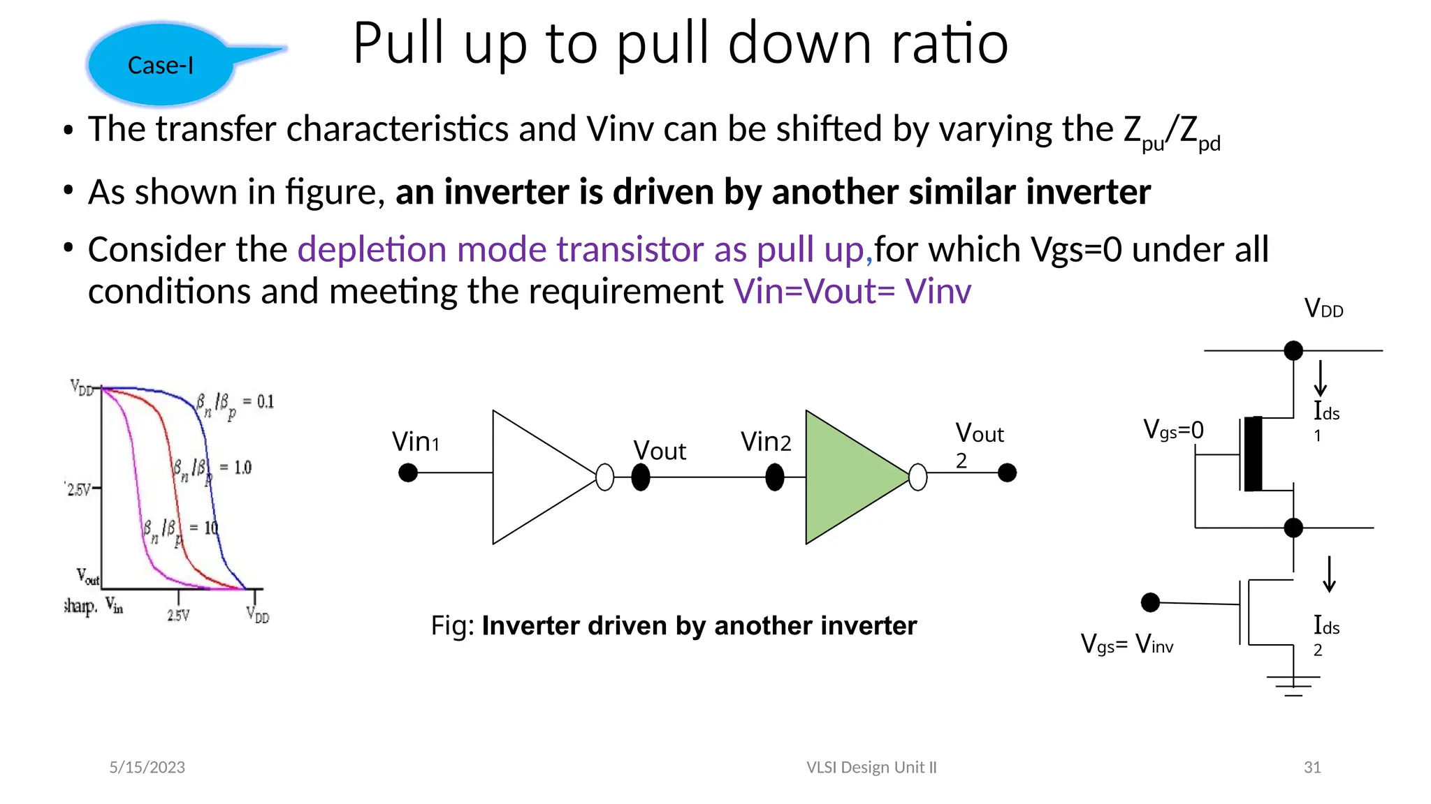
Aditya Engi
Basic Electrical Properties of Circuits:
• Ids versus Vds Relationships
• Aspects of MOS transistor: Vt, Gm, Gd, Figure of Merit,
• Pass Transistor concept ,
• NMOS Inverter, alternative forms of pull ups
• Pull-up to Pull-down Ratio for NMOS Inverter driven by another NMOS inverter,
• Pull-up to Pull-down Ratio for NMOS Inverter driven by another NMOS inverter
through one or more Pass Transistors.
• The CMOS Inverter, and Bi-CMOS Inverter,
• Transistor switches,
• Schematics using NMOS, PMOS, and CMOS technologies:
Inverter
NAND gate
NOR gate
UNIT-I
1
MOS diagrams
P-Sub
p-,n-
lightly doped
P+,n+
heavily
dopde
p,n
moderately
doped
P substrate
N+ N+
metal
Oxide
• nMOS enhancement mode
Vgs > Vth
holes
e-,e-
Vds> (Vgs-Vth)
Ids> 0
2
Summary of normal conduction characteristics:
 Cut-off : accumulation, Ids is essentially zero.
 Non-saturated : weak inversion, Ids dependent on both Vgs and Vds .
 Saturated : strong inversion, Ids is ideally independent of Vds.
Region NMOS
Non-saturation/
Triode
VDS < VDS(sat)
I  k' W 
(V V )V 
1
V 2

TN DS
2
DS
R 
VDS
DSon
I
D
Saturation/
Pinch-off
VDS > VDS(sat)
k '
 W  2
ID  n
 [VGS VTN ] 2 
L 
Transition between triode
and pinch-off
VDS(sat) = VGS - VTN
7
Ids vs Vds derivation
• A voltage on the gate, Vgs, induces a charge in the channel between source and drain
which may then caused electron to move from source to drain under the influence
of electric field created by drain voltage Vds.
• Since the charge induced is dependent on the gate -to-source voltage Vgs, then the Ids is
dependent on both Vgs and Vds.
• Consider the structure, as shown in figure below, in which electron will flow from source -
to- drain
8
• The drain to source current Ids is
I
• Where
• But velocity of moving particle
is between drain and the
source ,
and hence electron velocity
• There fore which is then given by

chargeinduced in a channel (Qc )
ds -sd

I sd
Electron transit time( )
Electron velocity (v)

Length of the channel(L)
sd

v  n Eds with an effective field developed
L
Vds
Eds 
L
Vds
v 
n
L
Vds
n

L
sd

 n ds

V
sd
L2


where n  650 cm2
/ v s and
p  240 cm2
/ v s
9
The Non-Saturation region:
• Where Qo is the charge per unit area which is given
by
and
• Eg is average electric field in the gate to channel and is given by
• The total induced charge (Qc) in the channel is then given by Qc  Q0WL
Q0 
Egins0
V
D D D
V
d s
g s t
g
E g




V  V 


 V


V d s
  
  
 G
2 2
ins is the relative permittivity of the
insulation
 0 is the absolute permittivity
Vg is the effective gate voltage = Vgs-Vt
Vds/2 is the average voltage at drain terminal
Vt is the threshold voltage
W is the width of the MOS transistor
L is the length of the MOS transistor
VG is the gate voltage under Vds 10
• The total induced charge (Qc) in the channel is then given
by
• Thus the drain - to - source current is given by
V d s
g s t 




D

V  V 
2
i n s 0
Q c    W L .
g s t
s d
c
n V d s
Q
I d s

2
i n s 0
L
2
  W L .





D
 
V d s

V  V



L 2
1
2
n ds
ds
gs t
ins 0
V
I d s
. V





D

V  V 
  
WL.
ds
t
gs
n
ds
V
D 2
L2
ins 0
.V
ds




1

V  V 
I  WL. .


ds
t
gs
g n
ds
V
2
2 .V




 V 
I  C . .
1 
 C 
 A
D
o
r
o
r
VLSI Design
o
r
11
• In other words the same current is also given
by
The Saturation region:
• Saturation begins when
d s
g s t
d s
V
2
0 n . V
d s



L 
 I  C  .
W 
V  V 
Vds
 Vg s Vt
2
2





 .
V d s
2
 V d
s
L

W

 I d s  K .
2 



 .

L

W  2 V d s
2

V d s
2
 I d s  K .











2
2
2
d s
V
L

W
  
K .
L

W  2 V d s
2

V d s
2
 I d s  K .
2
2
2
 V g s
 V t 2


 V
 I d s   .  d s 
o
r
o
r
o
r
12
V-I characteristics of nMOS
The parameters that effect the magnitude of Ids are:
 The distance between source and drain (channel length).
 The channel width.
 The threshold voltage.
 The thickness of the gate oxide layer.
 The dielectric constant of the gate insulator.
 The carrier (electron or hole) mobility.
ds
t
gs
n
ds
V
D 2
L
1
2
ins 0
.V
d s





V  V 
I  WL. .


13
Aditya Engineering
Aspects of MOS Transistor: Threshold voltage: Vt
• The MOSFET conducts no current between its source and drain terminals unless
VGS is greater than Vt0.
• Increasing the gate-to-source voltage above and beyond Vt0 will not affect the
surface potential and the depletion region depth.
• The gate to source voltage, for which the concentration of electrons under the gate
is equal to the concentration of holes in the p-sub far from the gate called
the THRESHOLD VOLTAGE (Vt = Vgs) and is given by
VT  V F B  2F
ox
C
2s q N A (2F  VS B )
Flat band
voltage
Lot more to
know about the
Vt. If you wish,
go through the
link
14
From equations, threshold voltage may be varied by changing:
 The doping concentration (N A ).
 The oxide capacitance (C ox ).
 Surface state charge (Q fc ).
GS TH
m n ox
L
g   C
W
V
V 
For a short-channel MOSFET:
g m
Key factors influencing
the MOS Performance
Aspects of MOS Transistor: Transconductance, gm
• In most MOSFET applications, an input signal is the gate voltage VG and the output is
the drain current Id.
• The ability of MOSFET to amplify the signal is given by the output current /input voltage
ratio, the Transconductance,
• Transconductance (gm) is a measure of how much drain current changes wrt the
gate voltage.
• For amplifier applications, the MOSFET is usually operating in the saturation region.
For a long-channel MOSFET:
16
• The output conductance of a MOS device is defined as the ratio between
the change in output current to the change in output voltage.
• The output conductance in non saturation is given by
• and decreases with increase in Vds (gds is 0 for saturation region).
V g s  C o n s t a n t
ds
ds
 V

Id s
g
Aspects of MOS Transistor: Output Conductance, gds
gs t ds
ds n ox
L
V V
g   C
W
V 
Aspects of MOS Transistor: figure of merit wo
• Figure of merit is used obtain the frequency response characteristics of a MOS
device in presence of AC source at gate.
• rs & rd are ignored and all drops are zero
• The figure of merit is given by
0
0
3
2L2
2
C WL
L
g n ox gs t
m
C g
 
w 
3n Vgs Vt 
 C
W
V  V 
17
MOSFET Pass Characteristics
18
Switch logic and gate logic
• Switch logic is based on the pass transistor (PTL)or on the transmission gate logic(TGL).
• This approach is fast for small arrays and takes no static current from the supply rails.
• Hence power dissipation is small since current flows on switching only.
• Switch (or pass transistor) logic is similar to logic arrays based on relay contacts
• The designer can implement logics with expected features.
19
Switch logic and gate logic
• Switch logic is based on the pass transistor (PTL)or on the transmission gate logic(TGL).
• This approach is fast for small arrays and takes no static current from the supply rails.
• Hence power dissipation is small since current flows on switching only.
• Switch (or pass transistor) logic is similar to logic arrays based on relay contacts
• The designer can implement logics with expected features.
5/15/2023 VLSI Design Unit II 20
AND gate in PTL
Switch logic and gate logic
21
Ex Or gate in PT Logic
nMOS Inverter logic with
enhancement nMOS as load
5/15/2023 VLSI Design Unit II 22
Name the logic?
RTL Inverter logic DTL Inverter logic TTL Inverter logic nMOS Inverter logic with R as load
Bi-CMOS Inverter logic
CMOS Inverter logic
nMOS Inverter logic with
depletion nMOS as load
Source: https://www.falstad.com/circuit/
Inverter
nMOS inverter
Resistor as PU
PD
n/w
PU
n/w
Enhancement nMOS as
PU
PU
n/w
PU
n/w
PD
n/w
Vdd
Vss Vss
Vout
Vin
PD n/w
Vin
Rd
Vdd
Vss
Vou
t
Vou
t
Vdd
Depletion nMOS as
PU Vout
Vou
t
Vin
Vin
0.5Vdd
0.5Vdd
Vdd
Vtp
d
Vtp
u
Vtp
d
Even Resistor is
taking much of
silicon area
23
Both the
Transistor &
Resistor are
taking much
of silicon area
Vin
cMOS inverter
Vdd
Vin
PD
n/w
PU
n/w
Vou
t
 When Vin =0, then pMOS transistor(PU) is ON and nMOS transistor is off Vdd( logic 1)
 When Vin =1, then T3 is ON(T4 OFF) implies T1 ON (T2 OFF) and hence Vout= 0( logic 0)
 Good with large driving capability.
Vss 0.5Vdd
Vdd
Vou
t
Vin
Vinv
0.5Vdd
Vdd
Vou
t
Vin
Vinv
24
CMOS Inverter: DC Analysi
• Analyze DC Characteristics of CMOS Gates
by studying an Inverter
• DC Analysis
– DC value of a signal in static conditions
• DC Analysis of CMOS Inverter
– Vin, input voltage
– Vout, output voltage
– single power supply, VDD
– Ground reference
– find Vout = f(Vin)
• Voltage Transfer Characteristic (VTC)
– plot of Vout as a function of Vin
– vary Vin from 0 to VDD
– find Vout at each value of Vin
25
Inverter Voltage Transfer Characteristics
• Output High Voltage, VOH
– maximum output voltage
• occurs when input is low (Vin = 0V)
• pMOS is ON, nMOS is OFF
• pMOS pulls Vout to VDD
– VOH = VDD
• Output Low Voltage, VOL
– minimum output voltage
• occurs when input is high (Vin = VDD)
• pMOS is OFF, nMOS is ON
• nMOS pulls Vout to Ground
– VOL = 0 V
• Logic Swing
– Max swing of output signal
• VL = VOH - VOL
• VL = VDD
26
Inverter Voltage Transfer Characteristics
• Transition Region (between VOH and VOL)
– Vin low
• Vin < Vtn
– Mn in Cutoff, OFF
– Mp in Triode, Vout pulled to VDD
• Vin > Vtn < ~Vout
– Mn in Saturation, strong current
– Mp in Triode, VSG & current reducing
– Vout decreases via current through Mn
– Vin = Vout (mid point) ≈ ½ VDD
– Mn and Mp both in Saturation
– maximum current
at Vin = Vout
– Vin high
• Vin > ~Vout, Vin < VDD - |Vtp|
– Mn in Triode, Mp in Saturation
• Vin > VDD - |Vtp|
– Mn in Triode, Mp in Cutoff
• Gate Voltage, f(Vin) •Drain Voltage,
f(Vout)
– VGSn=Vin, VSGp=VDD-Vin
Vin < VIL
input logic
LOW
Vin > VIH
input logic
HIGH
–VDSn=Vout, VSDp=VDD-Vout
+
VSGp
-
+ VGSn
-
27
Beta Ratios
Region C is the most important region. A small change in the input voltage, V in , results in a
LARGE change in the output voltage, V out .
This behavior describes an amplifier, the input is amplified at the output. The amplification is
termed transistor gain, which is given by beta.
Both the n and p-channel transistors have a beta.
their ratio will change the characteristics of the output
5
/ 1 5
/
28
29
Bi-cMOS inverter
 When Vin =0, then T4 is ON(T3 OFF) implies T2 ON (T1 OFF) and hence Vout= Vdd(
logic 1)
 When Vin =1, then T3 is ON(T4 OFF) implies T1 ON (T2 OFF) and hence Vout= 0( logic
0)
 Good with large driving capability.
Vdd
Vou
t
Vin=
Vss
T1
T2
T4
T3
0
1
ON ON
5/15/2023 30
VLSI Design Unit II
Pull up to pull down ratio
• The transfer characteristics and Vinv can be shifted by varying the Zpu/Zpd
• As shown in figure, an inverter is driven by another similar inverter
• Consider the depletion mode transistor as pull up,for which Vgs=0 under all
conditions and meeting the requirement Vin=Vout= Vinv
Vin1 Vin2
Vout
1
Vout
2
VDD
Vgs=0
Vgs= Vinv
Ids
1
Ids
2
Case-I
Fig: Inverter driven by another inverter
5/15/2023 VLSI Design Unit II 31
Pull up to pull down ratio
• Let us consider at Vg=Vin=Vinv=0.5VDD, both the transistors in an inverter are
in saturation with a drain current of;
• In depletion mode tr(PUN), the drain current can be re written as
• and the current in the enhancement mode tr(PDN), is


2
t

I  K
gs
W

V

V
L
ds


2


2

 Vtd
I  K
L
W
pu
pu
ds
VDD
Vgs=0
Vgs= Vinv
Ids
1
Ids
2

2


2

Vinv Vt

I  K
L
W
pd
pd
ds
32
Pull up to pull down ratio
• In saturation, current in both the transistors are equal and hence
• This is pull up to pull down ratio of inverter driven by another inverter
2



2




2

2

W
L p d
W  Vt d
 V i n v  V t
pu
L p u
p d 

pd
pd
pu
pu
td
pu
t
inv
pd W
and Z
W
Z
Z 
Lpd

Lpu
V V   V  ;Since,
Z
1
1 2
2
2
2
2
2
t
inv
/V V 
td
 V 
pd
pu
td
 V  
t
inv
V V 
pd
pu
Z
Z
Z
Z
V t d
t
 0.6V
V  0.2V
here;Vi n v  0.5V
1

4

Z p u
Z p d
33
Pull up to pull down ratio of ….. through one or more PTs
• Let us consider the arrangement shown in fig. input to inverter 2 is from output of
inverter 1, but through the series of nMOS transistors called Pass Transistors
Case-II
Fig: Inverter driven by another inverter through one or more Pass Transistors
Vout
1
Vout
2
Vin1
0
0
V
VDD
Vgs=0
Vgs= VDD
Ids
1
Ids
2
VDD
Vgs=0
Vgs= VDD-Vtp
Ids
1
Ids
2
(VDD-Vt1)-Vt2
-Vtp
VDD
V
VDD-Vt1 or
VDD
DD VDD
Vin
2
~1
1
<VDD
V
D
D
V
t
p
0
34
• We are now concerned that connection of pass transistors in series will degrade the logic 1 level
into inverter 2 so that the output will not be a proper logic 0 level.
• So as given in fig. input to inverter 2 is reduced by threshold voltage of series of nMOS pass
transistors.
• For this reduced voltage at input to inverter 2, we must get out the same as would be the output
of inverter 1.
R
1
Depletio
n
mode
Vout1=I1R
1
I
1
T1
Enhancemen
t mode
T
2
Vin=VDD
Fig: Inverter 1 with Vgs=Vin=
VDD
R
2 Vout2=I2R
2
I2
Enhancemen
t mode
T2
Vin=VDD-Vtp
T1
Depletio
n mode
Fig: Inverter 2 with Vgs=Vin= VDD-
Vtp
VDD
Vgs=0
Vgs= VDD
Ids
1
Ids
2
VDD
Vgs=0
Vgs= VDD-Vtp
Ids
1
Ids
2
35
• If the input is at VDD, then the pd transistor T2 is conducting but with a low voltage across it
,and is said to be linear mode or resistive mode represented by R1 shown in fig.
• But, Pu transistor T1 is in saturation and is said to be constant current source.
• For the Pd transistor,
• ; here Vgs=Vdd
• For the Pu transistor,
• ; here Vgs=0
2
Wpd1

Vds1

Ids  K
L (Vgs Vt )  Vds
1
pd1










 1

1
d s 1
2
D D t
p d 1
d s V
 (V  V ) 

1 L p d 1
K W
I

V d s 1
 R 1
 here Vds1 very small and hence
neglected


   (1)

pd1

ds1
Vt )

(VD
D
K
Ids
V
1
 R1   Z
Pull up to pull down ration Derivation
V
Wpd1


 Ids  K (VDD Vt )  ds1
Vds1
Lpd1

2

Lpu1
2
W  (VV )2 
pu1

gs
t
ds
I 
K



2
36
Wp u 1  (0 Vt d )2

 Ids  K 
Lpu1



1
2
p u 1
 (Vt d ) 2

I1  I d s  K
Z



    ( 2 )

1 1
Now Vout1  I
R



 V t 
 V D
D

td


Z p u 1

 K
K
X
1 1
Z p d 1

2
1  (  V )2

1
2


   (A)
) 2
 


td
 
 V t

  V
D D
 (  V
Z p u 1


Z p d 1
V o u t 1
2





 1 
   ( 3 )
N o w c o n s i d e r i n v e r t e r 2 w i t h i n p u t ( V D D  V t p )
t
t p
D D
p d 2
d s ( V  V  V )


1
Z
K
I

V d s 2
 R
2
1  (Vtd )2

and I2  Ids  K
Z

pu 2

    (4)

NowVout2  I2 R2 


 Vt p Vt

V
DD
K

td

X
 K
1
1
2
1  (V
Z p d 2

) 2

Z p u 2
 1
2


   (B)
) 2
 


td
 
VDD  V t p  V t
 (V
Z p u 2


Z p d 2
Vout 2
• And hence,
37
• If inverter 2 is to have the same output voltage under these conditions as inverter 1,then
Vout1= Vout2.
• ie… I1R1=I2R2
• Modifying the above equation, will give;
• Which leads
• For an inverter driven by another inverter is with and inverter driven by
another inverter through one or more Pass Transistor logic
with
is
desirable to have proper logic at o/p with expected amount of
shift













 td
td
Vtp Vt


VDD
Z Z 1
2
(V )
1
2 Vt

(V ) 2
Z pu 2

pd 2
2
Z pu1 
VDD
pd1
V V



V
Z Z
(VDD Vt )
pd1  DD tp
t 

Z pu1

pd 2
Z pu 2
at Vt  0.2VDD and Vtp  0.3VDD

4
2 
8
1
1
p d 2
Z
Z p u 2
1

4
Z p d
Z p u
1

8
Z p d
Z p u
38
Switch logic and gate logic
• Switch logic is based on the pass transistor (PTL)or on the transmission gate logic(TGL).
• This approach is fast for small arrays and takes no static current from the supply rails.
• Hence power dissipation is small since current flows on switching only.
• Switch (or pass transistor) logic is similar to logic arrays based on relay contacts
• The designer can implement logics with expected features.
5/15/2023 39
AND gate in PTL
Switch logic and gate logic
40
Ex Or gate in PT Logic
Vin Vou
t
Vdd
Vss
Vin
Vou
t
Vdd
Vss
CMOS inv
5/15/2023
VLSI Design Unit III P
. Bujjibabu, Associate Professor, ECE
41
Series/Parallel Equivalent Circuits
• Scale both W and L
– no effective change in
W/L
– increases gate
capacitance
inputs must be at same value/voltage
• Series Transistors
– increases effective
L
• Parallel Transistors
– increases
effective W
effective

½
effective

2
 = Cox
(W/L)
5/15/2023 VLSI Design Unit II 42
Consider above cited books for reference only and you may get more
information from some other books and websites
Collect notes from your subject Teacher, if interested.
Note:
http://emicroelectronics.free.fr/onlineCourses/VLSI/toc.html
http://ece-research.unm.edu/jimp/vlsi/slides/c1_itrs.pdf
http://rti.etf.bg.ac.rs/rti/ri5rvl/tutorial/TUTORIAL/HTML/HOMEPG.HTM
https://www.tutorialspoint.com/vlsi_design/vlsi_design_useful_resources.htm
https://www.southampton.ac.uk/~bim/notes/cad/
http://www.uta.edu/ronc/4345sp02/lectures/
http://www.ece.utep.edu/courses/web5392/Lab_7.html
http://www.ece.utep.edu/courses/web5392/Notes.html
http://www.ittc.ku.edu/~jstiles/312/handouts/
https://www.mepits.com/tutorial/384/vlsi/steps-for-ic-manufacturing
Useful Web links:
Aditya Engineering College (A)
5/15/2023 VLSI Design Unit II 43
P
. Bujjibabu, Associate Professor
,
ECE

Elecrical Propertiesddfafafafafafafav.pptx

  • 1.
    Aditya Engi Basic ElectricalProperties of Circuits: • Ids versus Vds Relationships • Aspects of MOS transistor: Vt, Gm, Gd, Figure of Merit, • Pass Transistor concept , • NMOS Inverter, alternative forms of pull ups • Pull-up to Pull-down Ratio for NMOS Inverter driven by another NMOS inverter, • Pull-up to Pull-down Ratio for NMOS Inverter driven by another NMOS inverter through one or more Pass Transistors. • The CMOS Inverter, and Bi-CMOS Inverter, • Transistor switches, • Schematics using NMOS, PMOS, and CMOS technologies: Inverter NAND gate NOR gate UNIT-I 1
  • 2.
    MOS diagrams P-Sub p-,n- lightly doped P+,n+ heavily dopde p,n moderately doped Psubstrate N+ N+ metal Oxide • nMOS enhancement mode Vgs > Vth holes e-,e- Vds> (Vgs-Vth) Ids> 0 2
  • 3.
    Summary of normalconduction characteristics:  Cut-off : accumulation, Ids is essentially zero.  Non-saturated : weak inversion, Ids dependent on both Vgs and Vds .  Saturated : strong inversion, Ids is ideally independent of Vds. Region NMOS Non-saturation/ Triode VDS < VDS(sat) I  k' W  (V V )V  1 V 2  TN DS 2 DS R  VDS DSon I D Saturation/ Pinch-off VDS > VDS(sat) k '  W  2 ID  n  [VGS VTN ] 2  L  Transition between triode and pinch-off VDS(sat) = VGS - VTN 7
  • 4.
    Ids vs Vdsderivation • A voltage on the gate, Vgs, induces a charge in the channel between source and drain which may then caused electron to move from source to drain under the influence of electric field created by drain voltage Vds. • Since the charge induced is dependent on the gate -to-source voltage Vgs, then the Ids is dependent on both Vgs and Vds. • Consider the structure, as shown in figure below, in which electron will flow from source - to- drain 8
  • 5.
    • The drainto source current Ids is I • Where • But velocity of moving particle is between drain and the source , and hence electron velocity • There fore which is then given by  chargeinduced in a channel (Qc ) ds -sd  I sd Electron transit time( ) Electron velocity (v)  Length of the channel(L) sd  v  n Eds with an effective field developed L Vds Eds  L Vds v  n L Vds n  L sd   n ds  V sd L2   where n  650 cm2 / v s and p  240 cm2 / v s 9
  • 6.
    The Non-Saturation region: •Where Qo is the charge per unit area which is given by and • Eg is average electric field in the gate to channel and is given by • The total induced charge (Qc) in the channel is then given by Qc  Q0WL Q0  Egins0 V D D D V d s g s t g E g     V  V     V   V d s        G 2 2 ins is the relative permittivity of the insulation  0 is the absolute permittivity Vg is the effective gate voltage = Vgs-Vt Vds/2 is the average voltage at drain terminal Vt is the threshold voltage W is the width of the MOS transistor L is the length of the MOS transistor VG is the gate voltage under Vds 10
  • 7.
    • The totalinduced charge (Qc) in the channel is then given by • Thus the drain - to - source current is given by V d s g s t      D  V  V  2 i n s 0 Q c    W L . g s t s d c n V d s Q I d s  2 i n s 0 L 2   W L .      D   V d s  V  V    L 2 1 2 n ds ds gs t ins 0 V I d s . V      D  V  V     WL. ds t gs n ds V D 2 L2 ins 0 .V ds     1  V  V  I  WL. .   ds t gs g n ds V 2 2 .V      V  I  C . . 1   C   A D o r o r VLSI Design o r 11
  • 8.
    • In otherwords the same current is also given by The Saturation region: • Saturation begins when d s g s t d s V 2 0 n . V d s    L   I  C  . W  V  V  Vds  Vg s Vt 2 2       . V d s 2  V d s L  W   I d s  K . 2      .  L  W  2 V d s 2  V d s 2  I d s  K .            2 2 2 d s V L  W    K . L  W  2 V d s 2  V d s 2  I d s  K . 2 2 2  V g s  V t 2    V  I d s   .  d s  o r o r o r 12
  • 9.
    V-I characteristics ofnMOS The parameters that effect the magnitude of Ids are:  The distance between source and drain (channel length).  The channel width.  The threshold voltage.  The thickness of the gate oxide layer.  The dielectric constant of the gate insulator.  The carrier (electron or hole) mobility. ds t gs n ds V D 2 L 1 2 ins 0 .V d s      V  V  I  WL. .   13
  • 10.
    Aditya Engineering Aspects ofMOS Transistor: Threshold voltage: Vt • The MOSFET conducts no current between its source and drain terminals unless VGS is greater than Vt0. • Increasing the gate-to-source voltage above and beyond Vt0 will not affect the surface potential and the depletion region depth. • The gate to source voltage, for which the concentration of electrons under the gate is equal to the concentration of holes in the p-sub far from the gate called the THRESHOLD VOLTAGE (Vt = Vgs) and is given by VT  V F B  2F ox C 2s q N A (2F  VS B ) Flat band voltage Lot more to know about the Vt. If you wish, go through the link 14 From equations, threshold voltage may be varied by changing:  The doping concentration (N A ).  The oxide capacitance (C ox ).  Surface state charge (Q fc ).
  • 11.
    GS TH m nox L g   C W V V  For a short-channel MOSFET: g m Key factors influencing the MOS Performance Aspects of MOS Transistor: Transconductance, gm • In most MOSFET applications, an input signal is the gate voltage VG and the output is the drain current Id. • The ability of MOSFET to amplify the signal is given by the output current /input voltage ratio, the Transconductance, • Transconductance (gm) is a measure of how much drain current changes wrt the gate voltage. • For amplifier applications, the MOSFET is usually operating in the saturation region. For a long-channel MOSFET: 16
  • 12.
    • The outputconductance of a MOS device is defined as the ratio between the change in output current to the change in output voltage. • The output conductance in non saturation is given by • and decreases with increase in Vds (gds is 0 for saturation region). V g s  C o n s t a n t ds ds  V  Id s g Aspects of MOS Transistor: Output Conductance, gds gs t ds ds n ox L V V g   C W V  Aspects of MOS Transistor: figure of merit wo • Figure of merit is used obtain the frequency response characteristics of a MOS device in presence of AC source at gate. • rs & rd are ignored and all drops are zero • The figure of merit is given by 0 0 3 2L2 2 C WL L g n ox gs t m C g   w  3n Vgs Vt   C W V  V  17
  • 13.
  • 14.
    Switch logic andgate logic • Switch logic is based on the pass transistor (PTL)or on the transmission gate logic(TGL). • This approach is fast for small arrays and takes no static current from the supply rails. • Hence power dissipation is small since current flows on switching only. • Switch (or pass transistor) logic is similar to logic arrays based on relay contacts • The designer can implement logics with expected features. 19
  • 15.
    Switch logic andgate logic • Switch logic is based on the pass transistor (PTL)or on the transmission gate logic(TGL). • This approach is fast for small arrays and takes no static current from the supply rails. • Hence power dissipation is small since current flows on switching only. • Switch (or pass transistor) logic is similar to logic arrays based on relay contacts • The designer can implement logics with expected features. 5/15/2023 VLSI Design Unit II 20 AND gate in PTL
  • 16.
    Switch logic andgate logic 21 Ex Or gate in PT Logic
  • 17.
    nMOS Inverter logicwith enhancement nMOS as load 5/15/2023 VLSI Design Unit II 22 Name the logic? RTL Inverter logic DTL Inverter logic TTL Inverter logic nMOS Inverter logic with R as load Bi-CMOS Inverter logic CMOS Inverter logic nMOS Inverter logic with depletion nMOS as load Source: https://www.falstad.com/circuit/ Inverter
  • 18.
    nMOS inverter Resistor asPU PD n/w PU n/w Enhancement nMOS as PU PU n/w PU n/w PD n/w Vdd Vss Vss Vout Vin PD n/w Vin Rd Vdd Vss Vou t Vou t Vdd Depletion nMOS as PU Vout Vou t Vin Vin 0.5Vdd 0.5Vdd Vdd Vtp d Vtp u Vtp d Even Resistor is taking much of silicon area 23 Both the Transistor & Resistor are taking much of silicon area Vin
  • 19.
    cMOS inverter Vdd Vin PD n/w PU n/w Vou t  WhenVin =0, then pMOS transistor(PU) is ON and nMOS transistor is off Vdd( logic 1)  When Vin =1, then T3 is ON(T4 OFF) implies T1 ON (T2 OFF) and hence Vout= 0( logic 0)  Good with large driving capability. Vss 0.5Vdd Vdd Vou t Vin Vinv 0.5Vdd Vdd Vou t Vin Vinv 24
  • 20.
    CMOS Inverter: DCAnalysi • Analyze DC Characteristics of CMOS Gates by studying an Inverter • DC Analysis – DC value of a signal in static conditions • DC Analysis of CMOS Inverter – Vin, input voltage – Vout, output voltage – single power supply, VDD – Ground reference – find Vout = f(Vin) • Voltage Transfer Characteristic (VTC) – plot of Vout as a function of Vin – vary Vin from 0 to VDD – find Vout at each value of Vin 25
  • 21.
    Inverter Voltage TransferCharacteristics • Output High Voltage, VOH – maximum output voltage • occurs when input is low (Vin = 0V) • pMOS is ON, nMOS is OFF • pMOS pulls Vout to VDD – VOH = VDD • Output Low Voltage, VOL – minimum output voltage • occurs when input is high (Vin = VDD) • pMOS is OFF, nMOS is ON • nMOS pulls Vout to Ground – VOL = 0 V • Logic Swing – Max swing of output signal • VL = VOH - VOL • VL = VDD 26
  • 22.
    Inverter Voltage TransferCharacteristics • Transition Region (between VOH and VOL) – Vin low • Vin < Vtn – Mn in Cutoff, OFF – Mp in Triode, Vout pulled to VDD • Vin > Vtn < ~Vout – Mn in Saturation, strong current – Mp in Triode, VSG & current reducing – Vout decreases via current through Mn – Vin = Vout (mid point) ≈ ½ VDD – Mn and Mp both in Saturation – maximum current at Vin = Vout – Vin high • Vin > ~Vout, Vin < VDD - |Vtp| – Mn in Triode, Mp in Saturation • Vin > VDD - |Vtp| – Mn in Triode, Mp in Cutoff • Gate Voltage, f(Vin) •Drain Voltage, f(Vout) – VGSn=Vin, VSGp=VDD-Vin Vin < VIL input logic LOW Vin > VIH input logic HIGH –VDSn=Vout, VSDp=VDD-Vout + VSGp - + VGSn - 27
  • 23.
    Beta Ratios Region Cis the most important region. A small change in the input voltage, V in , results in a LARGE change in the output voltage, V out . This behavior describes an amplifier, the input is amplified at the output. The amplification is termed transistor gain, which is given by beta. Both the n and p-channel transistors have a beta. their ratio will change the characteristics of the output 5 / 1 5 / 28
  • 24.
  • 25.
    Bi-cMOS inverter  WhenVin =0, then T4 is ON(T3 OFF) implies T2 ON (T1 OFF) and hence Vout= Vdd( logic 1)  When Vin =1, then T3 is ON(T4 OFF) implies T1 ON (T2 OFF) and hence Vout= 0( logic 0)  Good with large driving capability. Vdd Vou t Vin= Vss T1 T2 T4 T3 0 1 ON ON 5/15/2023 30 VLSI Design Unit II
  • 26.
    Pull up topull down ratio • The transfer characteristics and Vinv can be shifted by varying the Zpu/Zpd • As shown in figure, an inverter is driven by another similar inverter • Consider the depletion mode transistor as pull up,for which Vgs=0 under all conditions and meeting the requirement Vin=Vout= Vinv Vin1 Vin2 Vout 1 Vout 2 VDD Vgs=0 Vgs= Vinv Ids 1 Ids 2 Case-I Fig: Inverter driven by another inverter 5/15/2023 VLSI Design Unit II 31
  • 27.
    Pull up topull down ratio • Let us consider at Vg=Vin=Vinv=0.5VDD, both the transistors in an inverter are in saturation with a drain current of; • In depletion mode tr(PUN), the drain current can be re written as • and the current in the enhancement mode tr(PDN), is   2 t  I  K gs W  V  V L ds   2   2   Vtd I  K L W pu pu ds VDD Vgs=0 Vgs= Vinv Ids 1 Ids 2  2   2  Vinv Vt  I  K L W pd pd ds 32
  • 28.
    Pull up topull down ratio • In saturation, current in both the transistors are equal and hence • This is pull up to pull down ratio of inverter driven by another inverter 2    2     2  2  W L p d W  Vt d  V i n v  V t pu L p u p d   pd pd pu pu td pu t inv pd W and Z W Z Z  Lpd  Lpu V V   V  ;Since, Z 1 1 2 2 2 2 2 2 t inv /V V  td  V  pd pu td  V   t inv V V  pd pu Z Z Z Z V t d t  0.6V V  0.2V here;Vi n v  0.5V 1  4  Z p u Z p d 33
  • 29.
    Pull up topull down ratio of ….. through one or more PTs • Let us consider the arrangement shown in fig. input to inverter 2 is from output of inverter 1, but through the series of nMOS transistors called Pass Transistors Case-II Fig: Inverter driven by another inverter through one or more Pass Transistors Vout 1 Vout 2 Vin1 0 0 V VDD Vgs=0 Vgs= VDD Ids 1 Ids 2 VDD Vgs=0 Vgs= VDD-Vtp Ids 1 Ids 2 (VDD-Vt1)-Vt2 -Vtp VDD V VDD-Vt1 or VDD DD VDD Vin 2 ~1 1 <VDD V D D V t p 0 34
  • 30.
    • We arenow concerned that connection of pass transistors in series will degrade the logic 1 level into inverter 2 so that the output will not be a proper logic 0 level. • So as given in fig. input to inverter 2 is reduced by threshold voltage of series of nMOS pass transistors. • For this reduced voltage at input to inverter 2, we must get out the same as would be the output of inverter 1. R 1 Depletio n mode Vout1=I1R 1 I 1 T1 Enhancemen t mode T 2 Vin=VDD Fig: Inverter 1 with Vgs=Vin= VDD R 2 Vout2=I2R 2 I2 Enhancemen t mode T2 Vin=VDD-Vtp T1 Depletio n mode Fig: Inverter 2 with Vgs=Vin= VDD- Vtp VDD Vgs=0 Vgs= VDD Ids 1 Ids 2 VDD Vgs=0 Vgs= VDD-Vtp Ids 1 Ids 2 35
  • 31.
    • If theinput is at VDD, then the pd transistor T2 is conducting but with a low voltage across it ,and is said to be linear mode or resistive mode represented by R1 shown in fig. • But, Pu transistor T1 is in saturation and is said to be constant current source. • For the Pd transistor, • ; here Vgs=Vdd • For the Pu transistor, • ; here Vgs=0 2 Wpd1  Vds1  Ids  K L (Vgs Vt )  Vds 1 pd1            1  1 d s 1 2 D D t p d 1 d s V  (V  V )   1 L p d 1 K W I  V d s 1  R 1  here Vds1 very small and hence neglected      (1)  pd1  ds1 Vt )  (VD D K Ids V 1  R1   Z Pull up to pull down ration Derivation V Wpd1    Ids  K (VDD Vt )  ds1 Vds1 Lpd1  2  Lpu1 2 W  (VV )2  pu1  gs t ds I  K    2 36 Wp u 1  (0 Vt d )2   Ids  K  Lpu1   
  • 32.
    1 2 p u 1 (Vt d ) 2  I1  I d s  K Z        ( 2 )  1 1 Now Vout1  I R     V t   V D D  td   Z p u 1   K K X 1 1 Z p d 1  2 1  (  V )2  1 2      (A) ) 2     td    V t    V D D  (  V Z p u 1   Z p d 1 V o u t 1 2       1     ( 3 ) N o w c o n s i d e r i n v e r t e r 2 w i t h i n p u t ( V D D  V t p ) t t p D D p d 2 d s ( V  V  V )   1 Z K I  V d s 2  R 2 1  (Vtd )2  and I2  Ids  K Z  pu 2      (4)  NowVout2  I2 R2     Vt p Vt  V DD K  td  X  K 1 1 2 1  (V Z p d 2  ) 2  Z p u 2  1 2      (B) ) 2     td   VDD  V t p  V t  (V Z p u 2   Z p d 2 Vout 2 • And hence, 37
  • 33.
    • If inverter2 is to have the same output voltage under these conditions as inverter 1,then Vout1= Vout2. • ie… I1R1=I2R2 • Modifying the above equation, will give; • Which leads • For an inverter driven by another inverter is with and inverter driven by another inverter through one or more Pass Transistor logic with is desirable to have proper logic at o/p with expected amount of shift               td td Vtp Vt   VDD Z Z 1 2 (V ) 1 2 Vt  (V ) 2 Z pu 2  pd 2 2 Z pu1  VDD pd1 V V    V Z Z (VDD Vt ) pd1  DD tp t   Z pu1  pd 2 Z pu 2 at Vt  0.2VDD and Vtp  0.3VDD  4 2  8 1 1 p d 2 Z Z p u 2 1  4 Z p d Z p u 1  8 Z p d Z p u 38
  • 34.
    Switch logic andgate logic • Switch logic is based on the pass transistor (PTL)or on the transmission gate logic(TGL). • This approach is fast for small arrays and takes no static current from the supply rails. • Hence power dissipation is small since current flows on switching only. • Switch (or pass transistor) logic is similar to logic arrays based on relay contacts • The designer can implement logics with expected features. 5/15/2023 39 AND gate in PTL
  • 35.
    Switch logic andgate logic 40 Ex Or gate in PT Logic
  • 36.
    Vin Vou t Vdd Vss Vin Vou t Vdd Vss CMOS inv 5/15/2023 VLSIDesign Unit III P . Bujjibabu, Associate Professor, ECE 41
  • 37.
    Series/Parallel Equivalent Circuits •Scale both W and L – no effective change in W/L – increases gate capacitance inputs must be at same value/voltage • Series Transistors – increases effective L • Parallel Transistors – increases effective W effective  ½ effective  2  = Cox (W/L) 5/15/2023 VLSI Design Unit II 42
  • 38.
    Consider above citedbooks for reference only and you may get more information from some other books and websites Collect notes from your subject Teacher, if interested. Note: http://emicroelectronics.free.fr/onlineCourses/VLSI/toc.html http://ece-research.unm.edu/jimp/vlsi/slides/c1_itrs.pdf http://rti.etf.bg.ac.rs/rti/ri5rvl/tutorial/TUTORIAL/HTML/HOMEPG.HTM https://www.tutorialspoint.com/vlsi_design/vlsi_design_useful_resources.htm https://www.southampton.ac.uk/~bim/notes/cad/ http://www.uta.edu/ronc/4345sp02/lectures/ http://www.ece.utep.edu/courses/web5392/Lab_7.html http://www.ece.utep.edu/courses/web5392/Notes.html http://www.ittc.ku.edu/~jstiles/312/handouts/ https://www.mepits.com/tutorial/384/vlsi/steps-for-ic-manufacturing Useful Web links: Aditya Engineering College (A) 5/15/2023 VLSI Design Unit II 43 P . Bujjibabu, Associate Professor , ECE