MOSFET In electronics, the metal–oxide–semiconductor field-effect transistor (MOSFET, MOS-FET, MOS FET, or MOS transistor) is a type of field-effect transistor (FET), most commonly fabricated by the controlled oxidation of silicon. It has an insulated gate, the voltage of which determines the conductivity of the device. This ability to change conductivity with the amount of applied voltage can be used for amplifying or switching electronic signals. The term metal–insulator–semiconductor field-effect transistor (MISFET) is almost synonymous with MOSFET. Another near-synonym is insulated-gate field-effect transistor (IGFET).In electronics, the metal–oxide–semiconductor field-effect transistor (MOSFET, MOS-FET, MOS FET, or MOS transistor) is a type of field-effect transistor (FET), most commonly fabricated by the controlled oxidation of silicon. It has an insulated gate, the voltage of which determines the conductivity of the device. This ability to change conductivity with the amount of applied voltage can be used for amplifying or switching electronic signals. The term metal–insulator–semiconductor field-effect transistor (MISFET) is almost synonymous with MOSFET. Another near-synonym is insulated-gate field-effect transistor (IGFET).In electronics, the metal–oxide–semiconductor field-effect transistor (MOSFET, MOS-FET, MOS FET, or MOS transistor) is a type of field-effect transistor (FET), most commonly fabricated by the controlled oxidation of silicon. It has an insulated gate, the voltage of which determines the conductivity of the device. This ability to change conductivity with the amount of applied voltage can be used for amplifying or switching electronic signals. The term metal–insulator–semiconductor field-effect transistor (MISFET) is almost synonymous with MOSFET. Another near-synonym is insulated-gate field-effect transistor (IGFET).In electronics, the metal–oxide–semiconductor field-effect transistor (MOSFET, MOS-FET, MOS FET, or MOS transistor) is a type of field-effect transistor (FET), most commonly fabricated by the controlled oxidation of silicon. It has an insulated gate, the voltage of which determines the conductivity of the device. This ability to change conductivity with the amount of applied voltage can be used for amplifying or switching electronic signals. The term metal–insulator–semiconductor field-effect transistor (MISFET) is almost synonymous with MOSFET. Another near-synonym is insulated-gate field-effect transistor (IGFET).In electronics, the metal–oxide–semiconductor field-effect transistor (MOSFET, MOS-FET, MOS FET, or MOS transistor) is a type of field-effect transistor (FET), most commonly fabricated by the controlled oxidation of silicon. It has an insulated gate, the voltage of which determines the conductivity of the device. This ability to change conductivity with the amount of applied voltage can be used for amplifying or switching electronic signals. The term metal–insulator–semiconductor field-effect tra
![Some important equations in the
inversion regime (Depth direction)
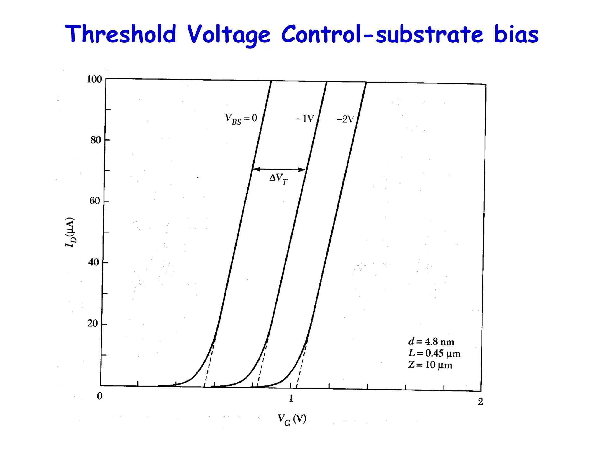
VT = ms + 2B + ox
Wdm = [2S(2B)/qNA]
Qinv = -Cox(VG - VT)
ox = Qs/Cox
Qs = qNAWdm
VT = ms + 2B + [4SBqNA]/Cox
Substrate
Channel Drain
Insulator
Gate
Source
x](https://image.slidesharecdn.com/mosfet-250321155844-51fa2d7f/75/MOSFET-operation-characteristics-and-types-3-2048.jpg)

![How to include y-dependent potentials?
S = 2B + V(y)
VG = S + [2SSqNA]/Cox
Need VG – V(y) > VT to invert
channel at y (V increases
threshold)
Since V(y) largest at drain end, that
end reverts from inversion to
depletion first (Pinch off)
SATURATION [VDSAT = VG – VT]](https://image.slidesharecdn.com/mosfet-250321155844-51fa2d7f/75/MOSFET-operation-characteristics-and-types-7-2048.jpg)
![j = qninvv = (Qinv/tinv)v
I = jA = jZtinv = ZQinvv
So current:
Qinv = -Cox[VG – VT - V(y)]
v = -effdV(y)/dy](https://image.slidesharecdn.com/mosfet-250321155844-51fa2d7f/75/MOSFET-operation-characteristics-and-types-8-2048.jpg)
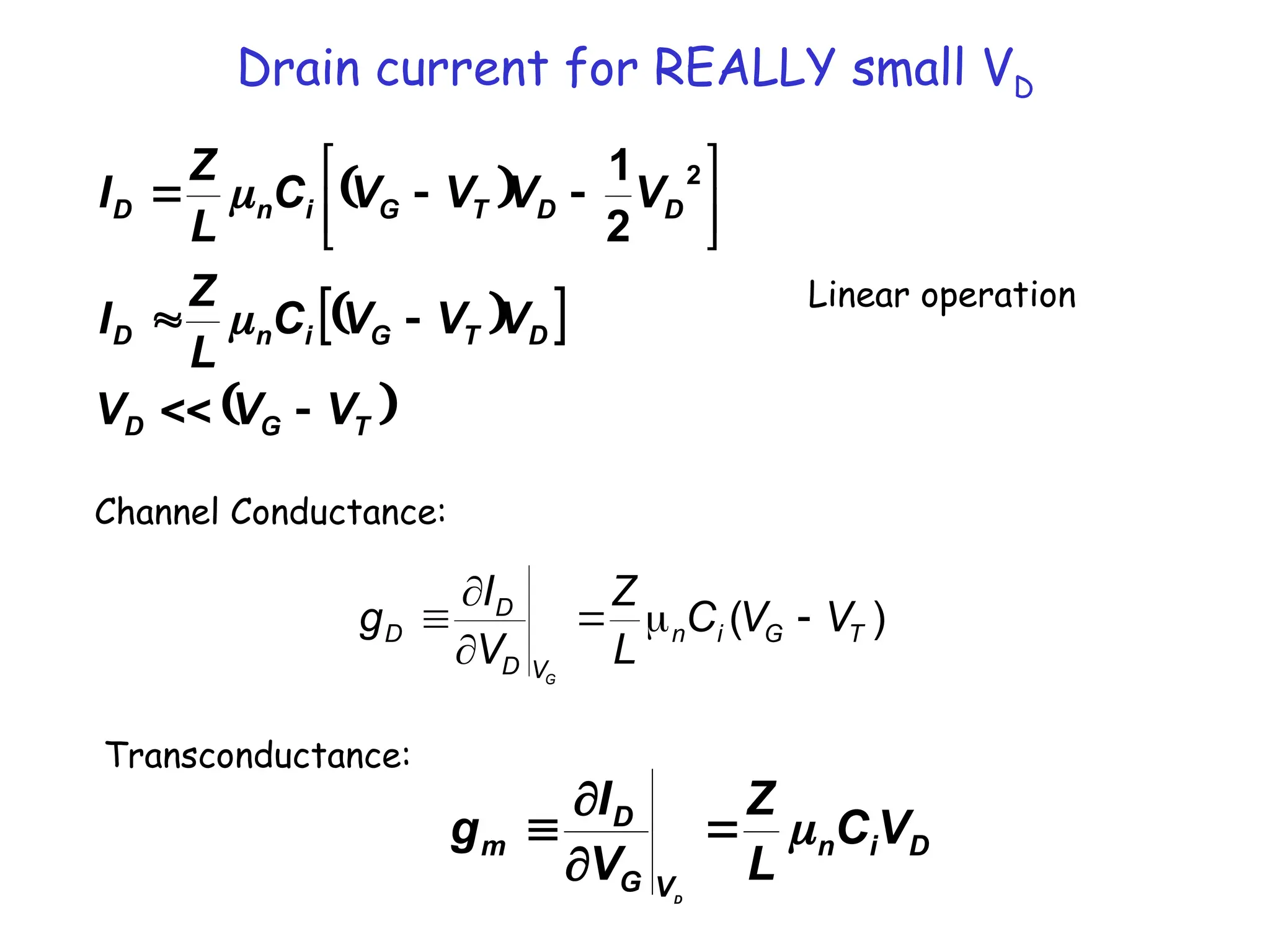
![So current:
I = eff ZCox[VG – VT - V(y)]dV(y)/dy
I = eff ZCox[(VG – VT )VD- VD
2
/2]/L
Continuity implies ∫Idy = IL](https://image.slidesharecdn.com/mosfet-250321155844-51fa2d7f/75/MOSFET-operation-characteristics-and-types-9-2048.jpg)
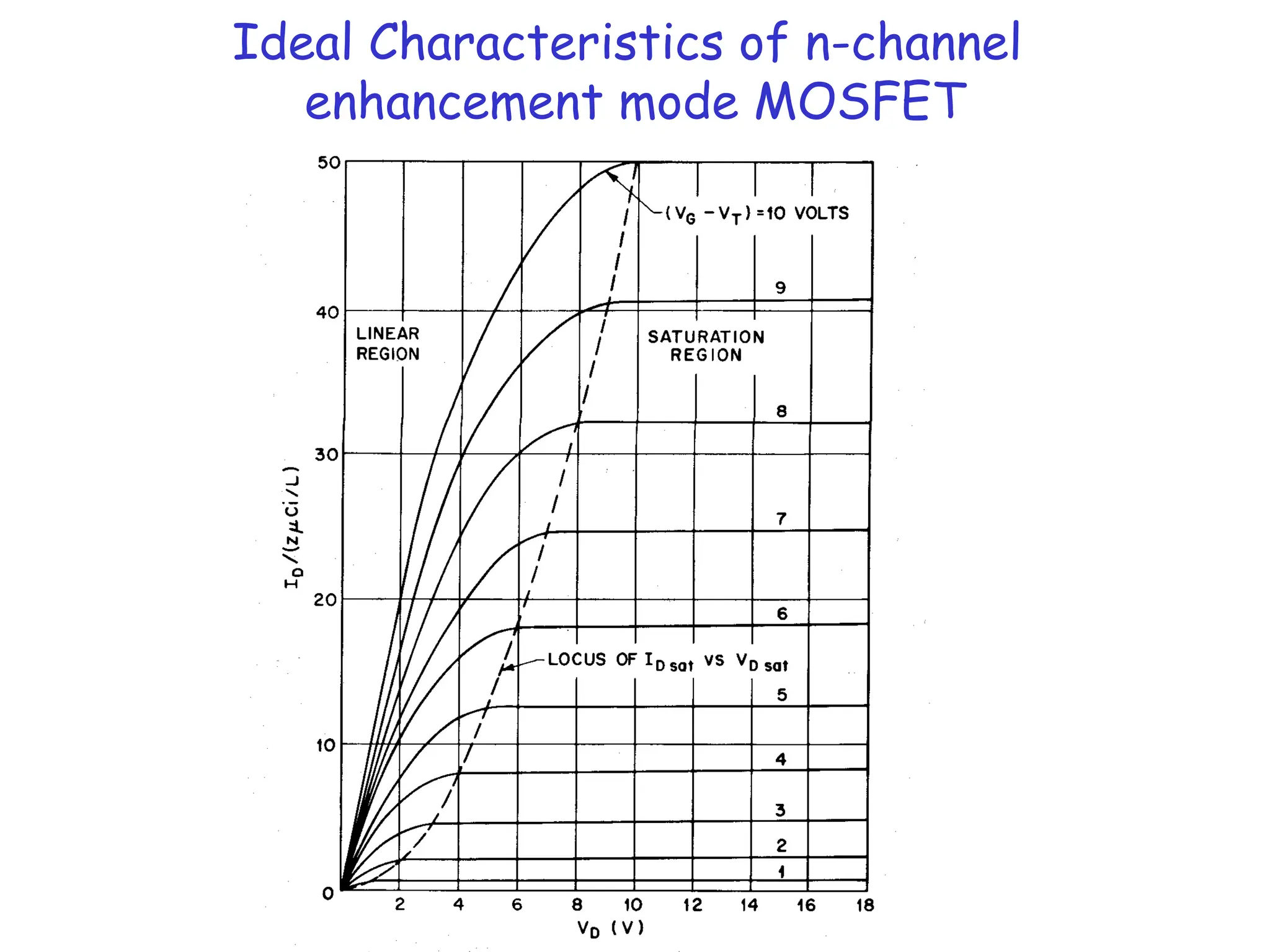
![But this current behaves like a parabola !!
ID
VD
IDsat
VDsat
I = eff ZCox[(VG – VT )VD- VD
2
/2]/L
We have assumed inversion in our model (ie, always above pinch-off)
So we just extend the maximum current into saturation…
Easy to check that above current is maximum for VDsat = VG - VT
Substituting, IDsat = (CoxeffZ/2L)(VG-VT)2](https://image.slidesharecdn.com/mosfet-250321155844-51fa2d7f/75/MOSFET-operation-characteristics-and-types-10-2048.jpg)
![Square law theory of MOSFETs
I = eff ZCox[(VG – VT )VD- VD
2
/2]/L, VD < VG - VT
I = eff ZCox(VG – VT )2
/2L, VD > VG - VT
J = qnv
n ~ Cox(VG – VT )
v ~ effVD /L
NEW](https://image.slidesharecdn.com/mosfet-250321155844-51fa2d7f/75/MOSFET-operation-characteristics-and-types-12-2048.jpg)


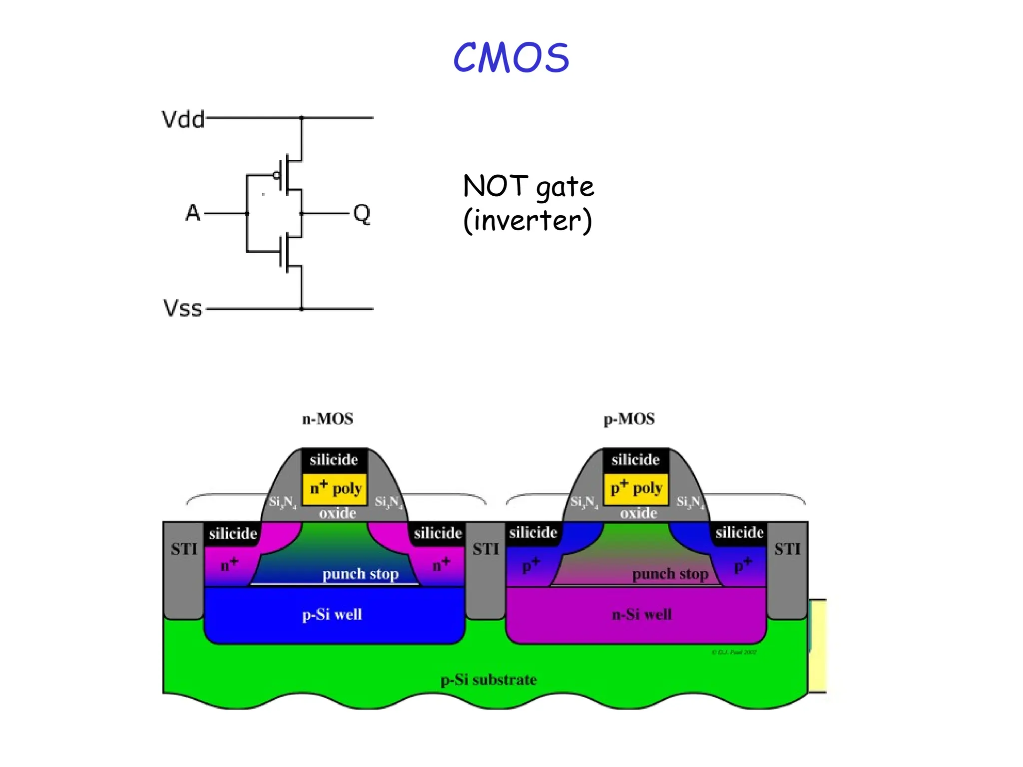
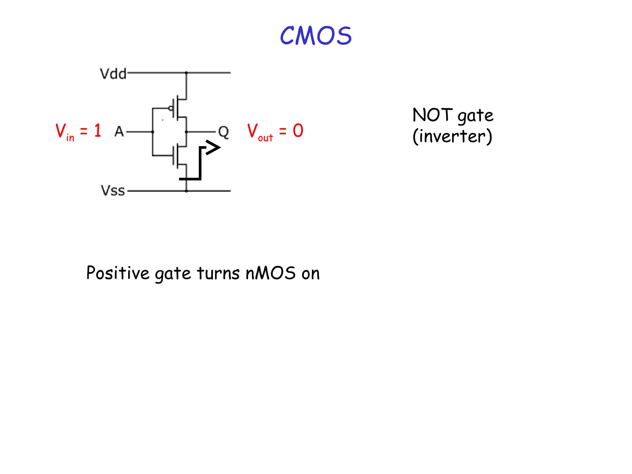
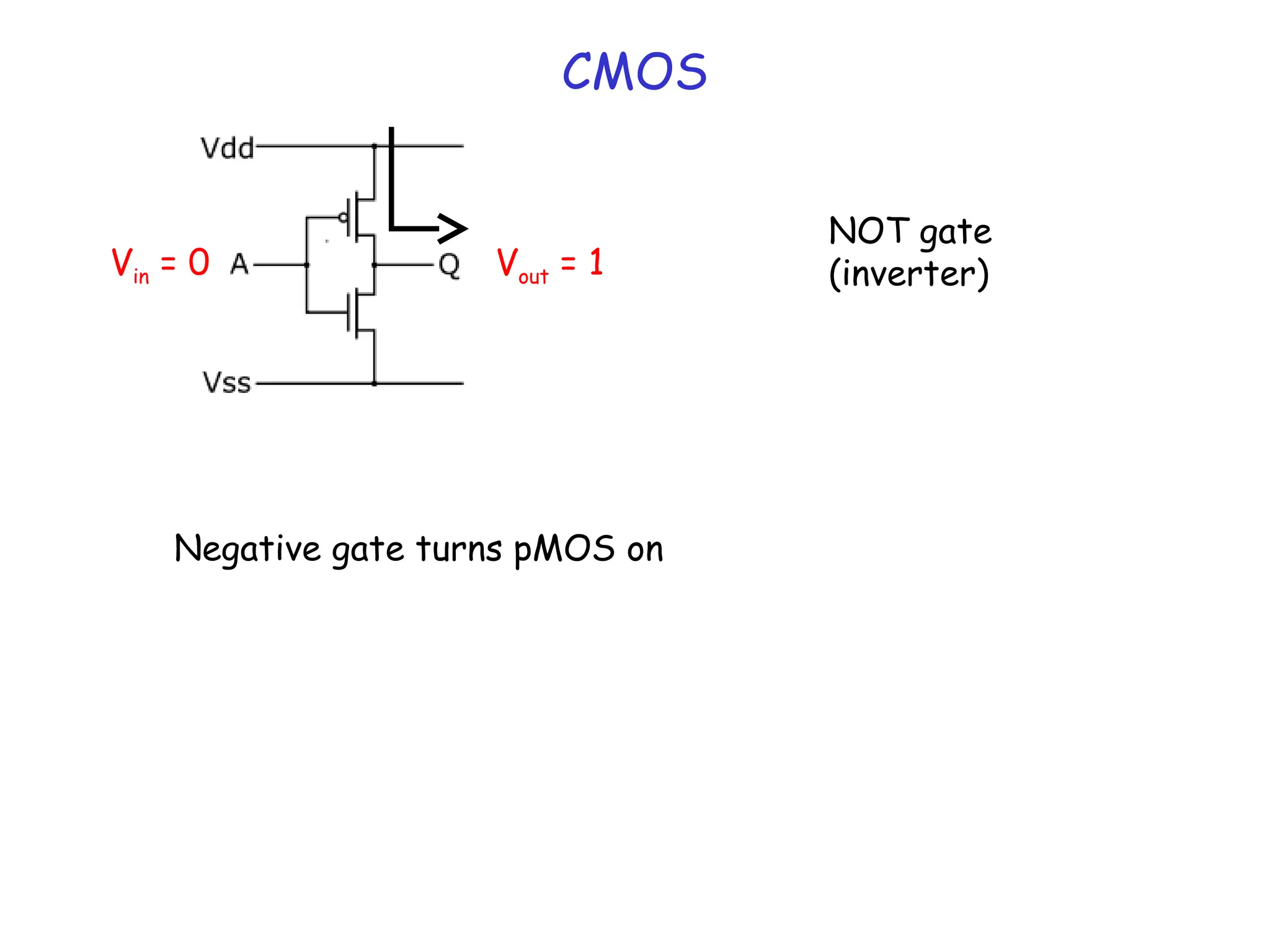
![BJT vs MOSFET
• RTL logic vs CMOS logic
• DC Input impedance of MOSFET (at gate end) is infinite
Thus, current output can drive many inputs FANOUT
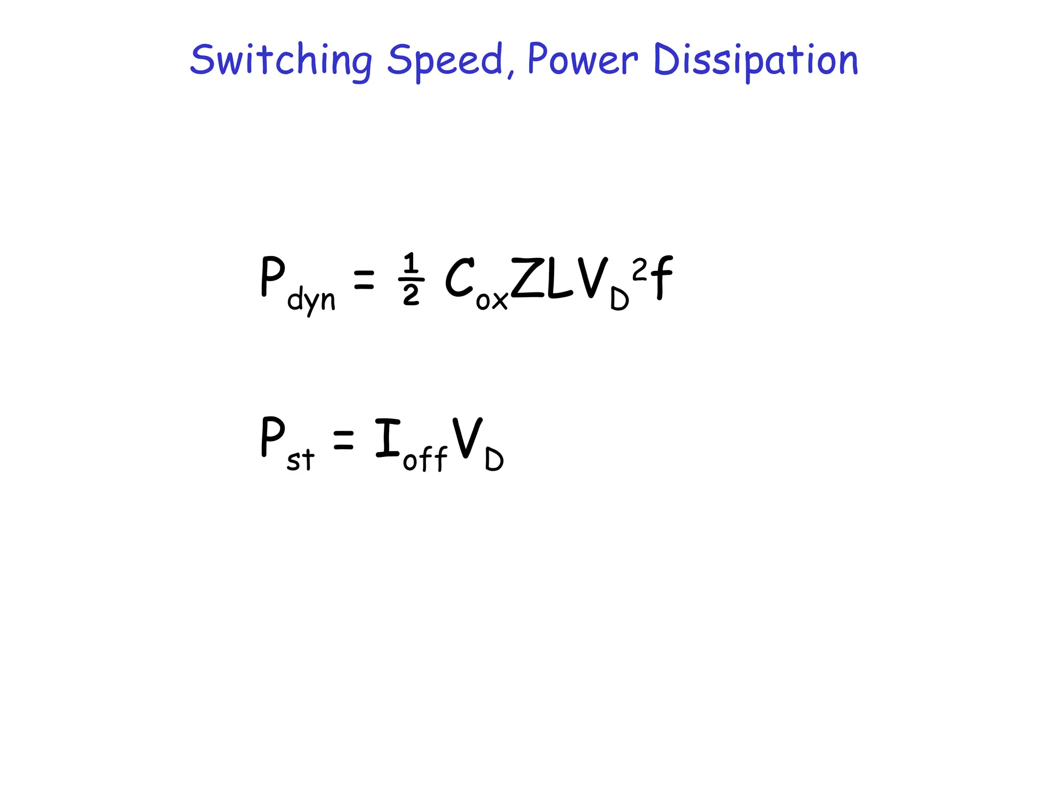
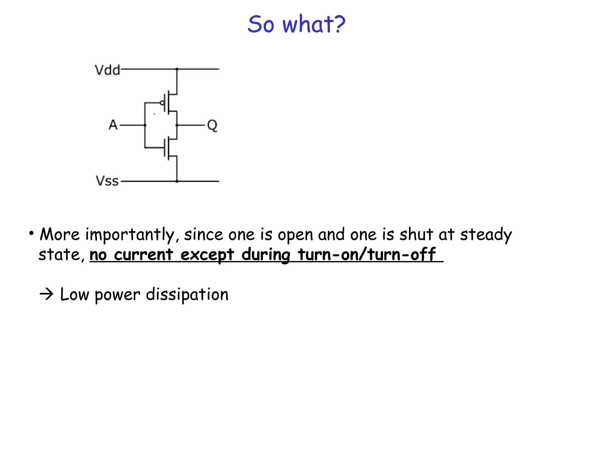
• CMOS static dissipation is low!! ~ IOFFVDD
• Normally BJTs have higher transconductance/current (faster!)
IC = (qni
2
Dn/WBND)exp(qVBE/kT) ID = CoxW(VG-VT) 2
/L
gm = IC/VBE = IC/(kT/q) gm = ID/VG = ID/[(VG-VT)/2]
• Today’s MOSFET ID >> IC due to near ballistic operation
NEW](https://image.slidesharecdn.com/mosfet-250321155844-51fa2d7f/75/MOSFET-operation-characteristics-and-types-32-2048.jpg)
![It also affects the I-V
VG
The threshold voltage is increased due to the depletion region
that grows at the drain end because the inversion layer shrinks
there and can’t screen it any more. (Wd > Wdm)
Qinv = -Cox[VG-VT(y)], I = -effZQinvdV(y)/dy
VT(y) = + √2sqNA/Cox
= 2B + V(y)](https://image.slidesharecdn.com/mosfet-250321155844-51fa2d7f/75/MOSFET-operation-characteristics-and-types-36-2048.jpg)
![It also affects the I-V
IL = ∫effZCox[VG – (2B+V) - √2sqNA(2B+V)/Cox]dV
I = (ZeffCox/L)[(VG–2B)VD –VD
2
/2
-2√2sqNA{(2B+VD)3/2
-(2B)3/2
}/3Cox]](https://image.slidesharecdn.com/mosfet-250321155844-51fa2d7f/75/MOSFET-operation-characteristics-and-types-37-2048.jpg)
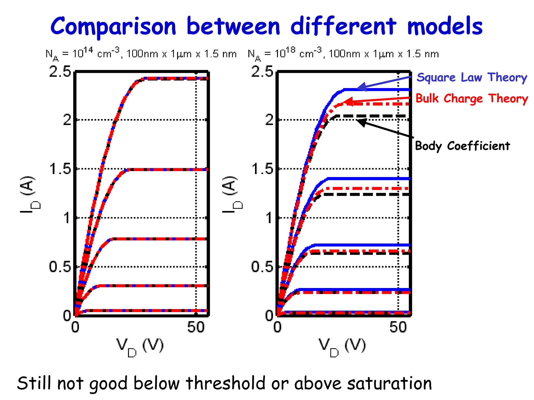
![We can approximately include this…
Include an additional charge term from the
depletion layer capacitance controlling V(y)
Q = -Cox[VG-VT]+(Cox + Cd)V(y)
where Cd = s/Wdm
Q = -Cox[VG –VT - MV(y)], M = 1 + Cd/Cox
ID = (ZeffCox/L)[(VG-VT - MVD/2)VD]](https://image.slidesharecdn.com/mosfet-250321155844-51fa2d7f/75/MOSFET-operation-characteristics-and-types-38-2048.jpg)


![Coded Agents – with UiPath SDK + LangGraph [Virtual Hands-on Workshop]](https://cdn.slidesharecdn.com/ss_thumbnails/codedagentsdeck-251215155422-5497c599-thumbnail.jpg?width=640&height=640&fit=bounds)


