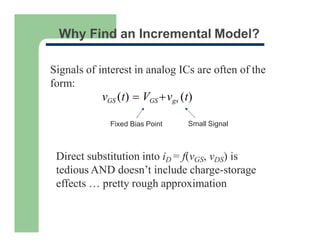
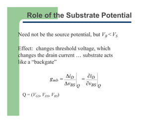
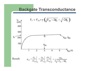
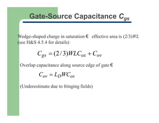
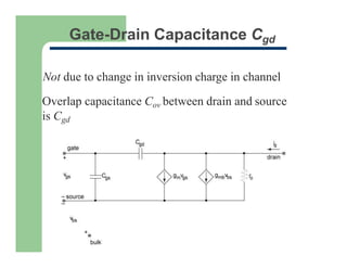
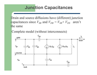
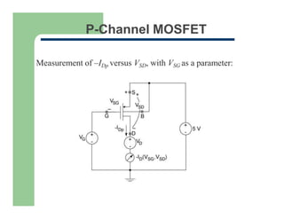
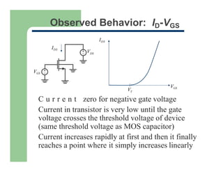
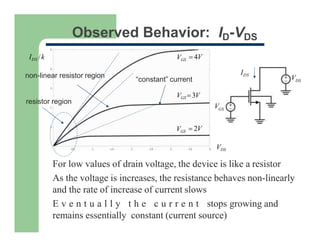
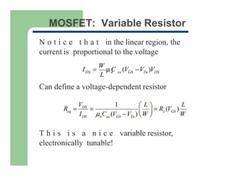
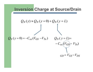
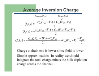
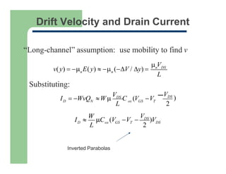
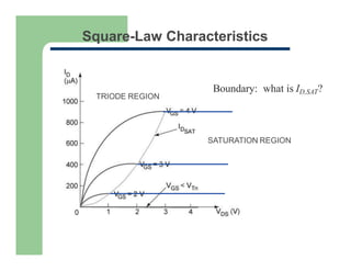
The document discusses MOS transistor models and behavior. It describes:
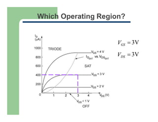
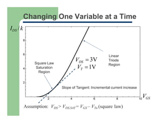
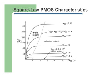
1) The I-V characteristics of MOS transistors, including the square-law model and linear region behavior as gate voltage exceeds threshold.
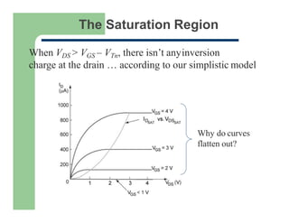
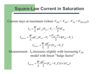
2) The saturation region where drain current reaches a maximum and becomes independent of drain-source voltage.
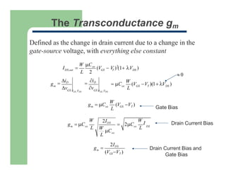
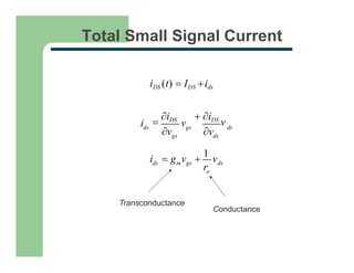
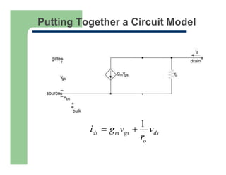
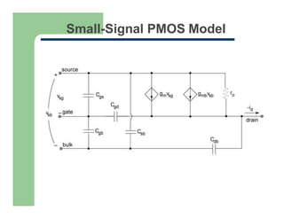
3) The linear small-signal model of the MOSFET as a voltage-controlled resistor with transconductance gm.
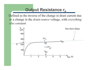
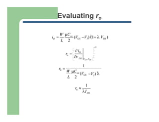
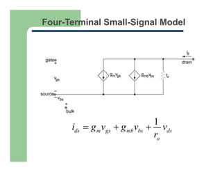
4) The development of a four-terminal small-signal model including transconductance gm, output resistance ro, and backgate transconductance gmb.


![Linear MOSFET Model
Channel (inversion) charge: neglect reduction at drain
Velocity saturation defines VDS,SAT = Esat L =constant
- vsat /n
Drain current:
ID,SAT WvQN W (vsat)[Cox (VGS VTn )],
|Esat| = 104 V/cm, L = 0.12 m € VDS,SAT = 0.12 V!
ID,SAT vsatWCox (VGS VTn)(1 nVDS )](https://image.slidesharecdn.com/idsmosequation1-231225121740-ce33db06/85/IDS-MOS-Equation-1-pptx-15-320.jpg)