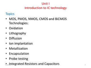
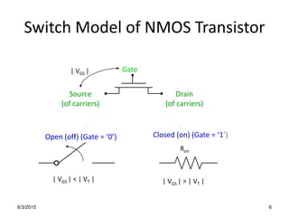
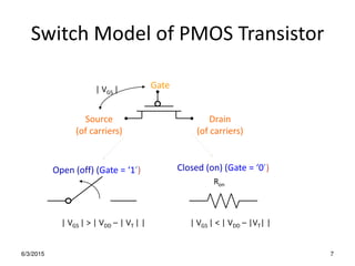
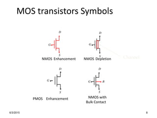
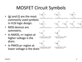
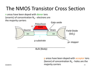
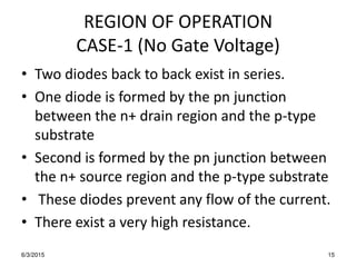
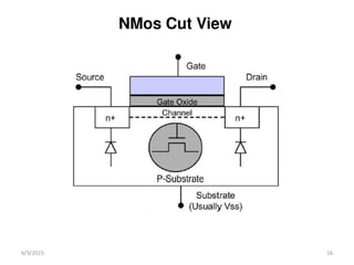
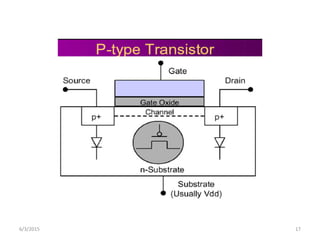
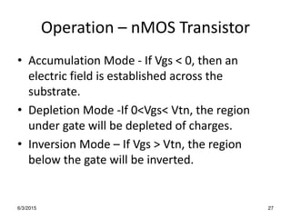
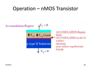
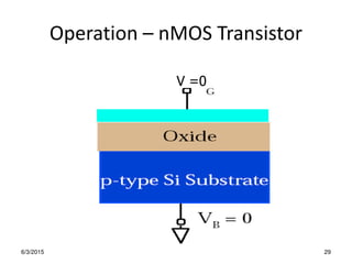
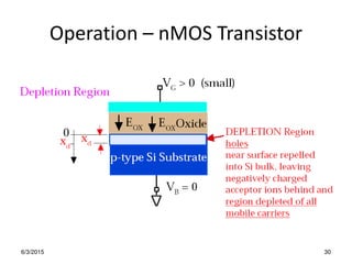
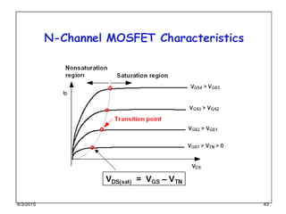
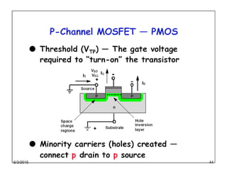
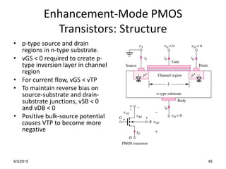
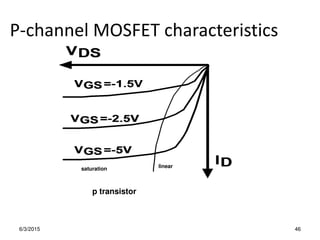
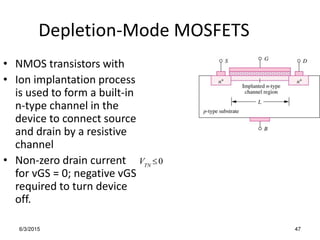
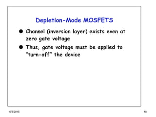
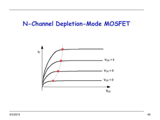
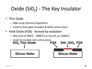
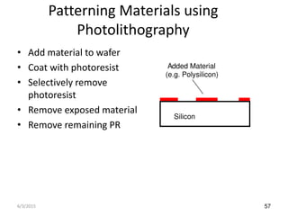
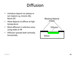
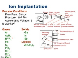
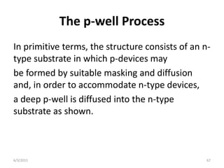
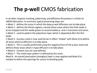
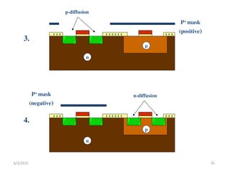
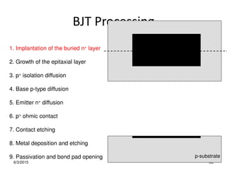
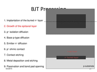
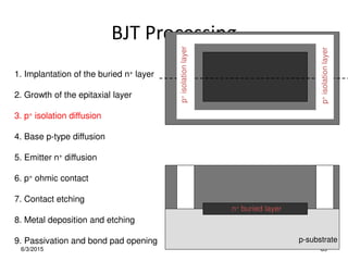
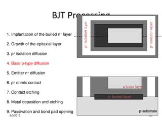
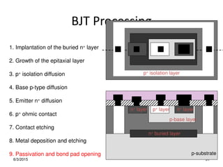
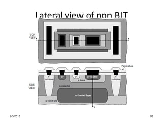
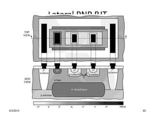
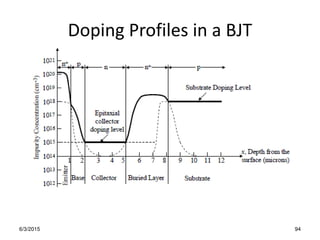
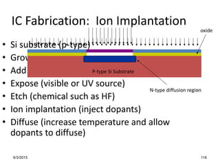
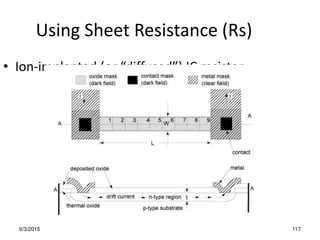
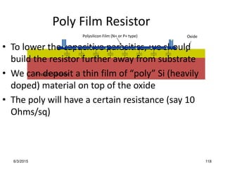
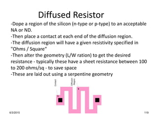
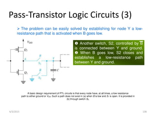
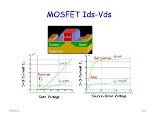
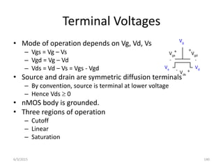
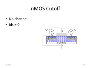
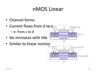
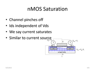
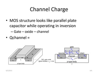
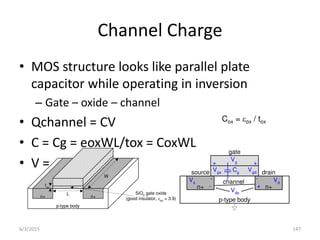
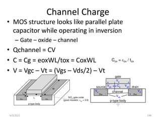
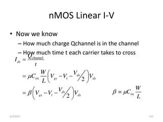
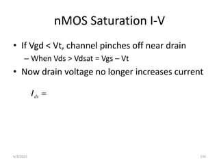
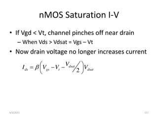
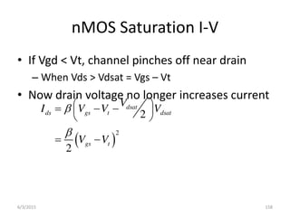
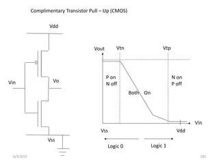
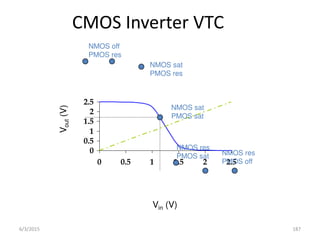
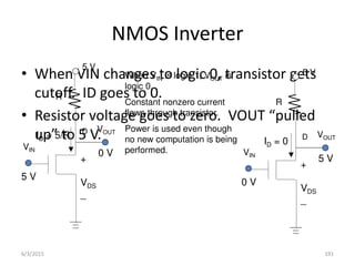
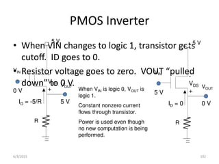
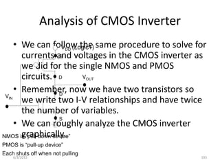
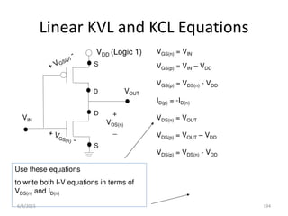
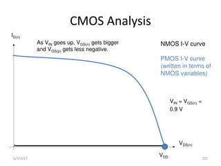
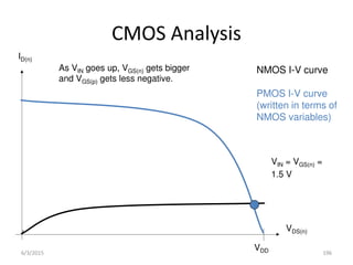
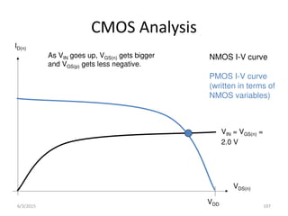
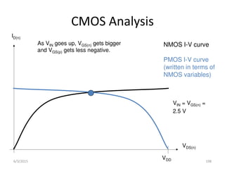
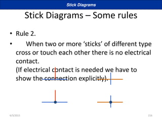
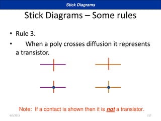
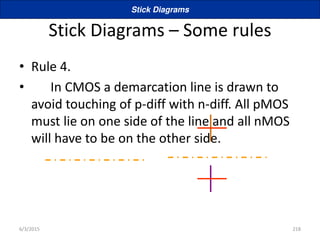
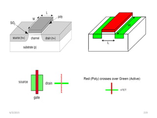
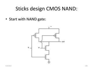
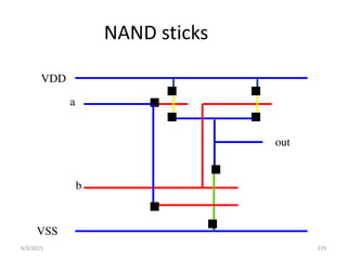
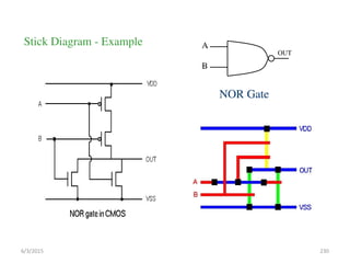
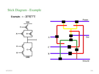
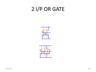
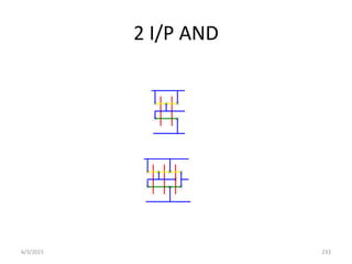
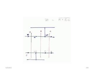
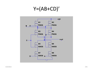
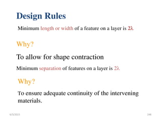
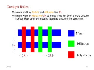
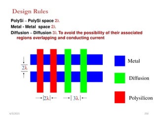
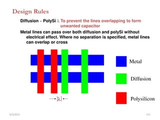
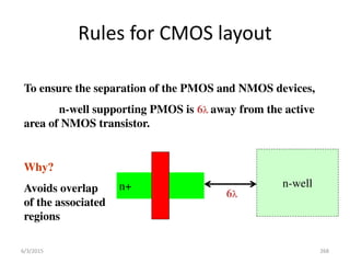
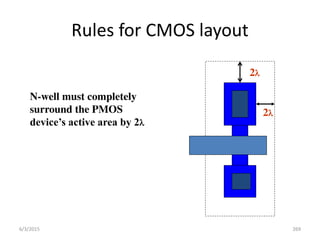
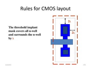
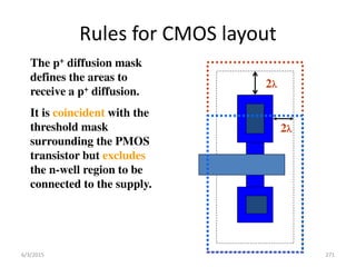
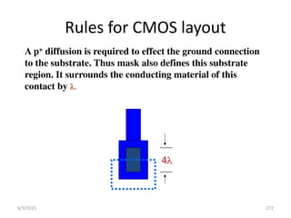
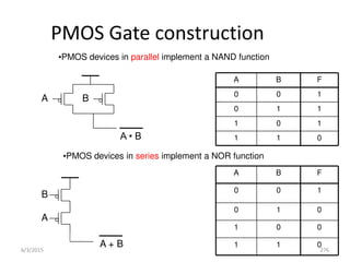
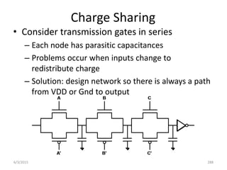
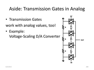
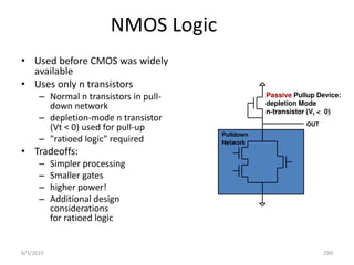
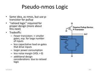
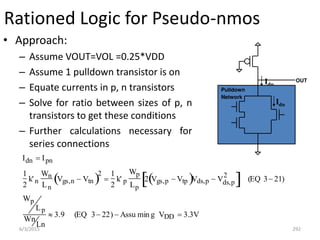
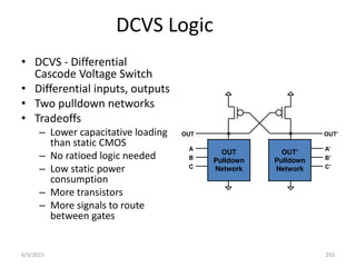
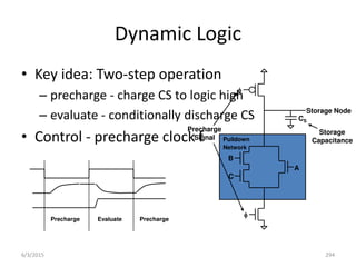
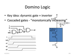
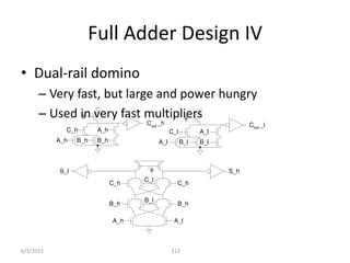
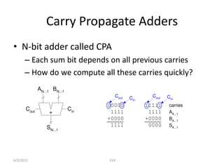
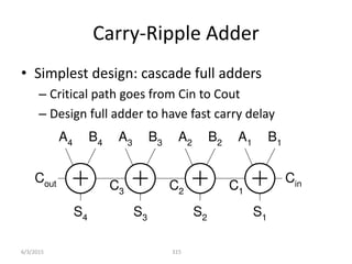
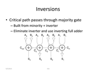
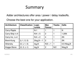
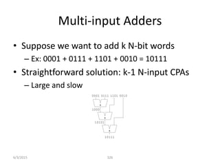
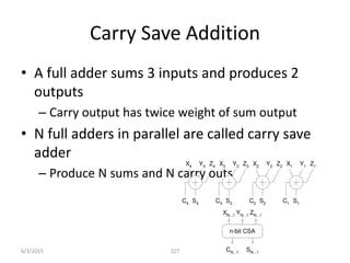
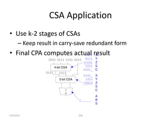
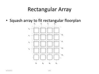
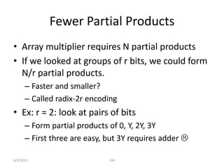
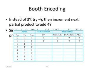
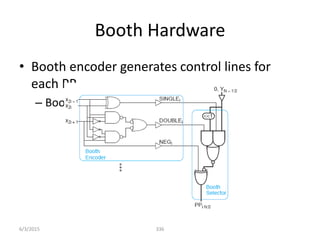
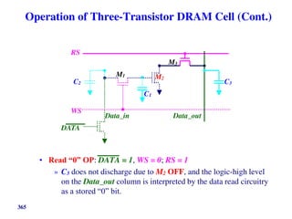
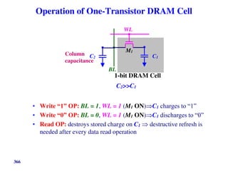
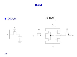
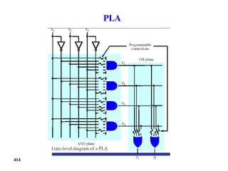
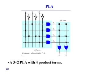
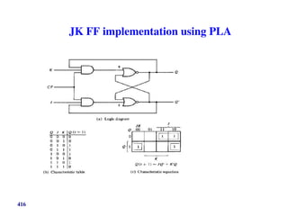
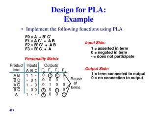
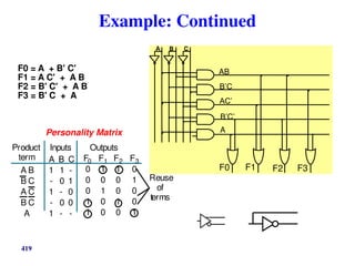
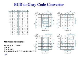
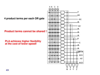
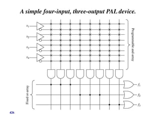
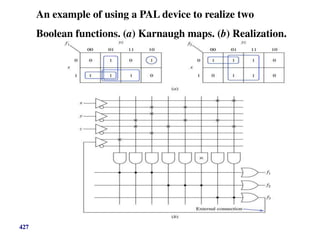
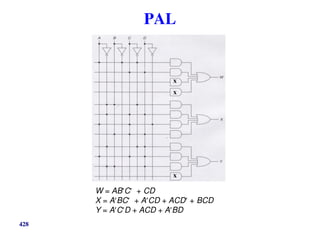
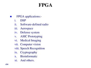
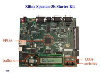
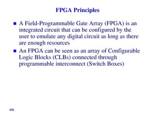
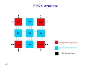
The document outlines the lecture slides for a course on VLSI Design. It covers topics such as introduction to IC technology including various processes like oxidation, lithography, diffusion, and doping. It also discusses MOSFET basics like different types of MOS transistors, their symbols, characteristics and modes of operation. The summary provides an overview of the key concepts covered in the VLSI Design lecture.


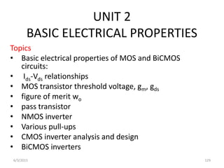
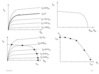
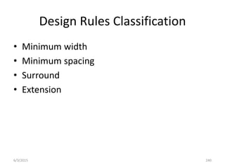
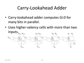
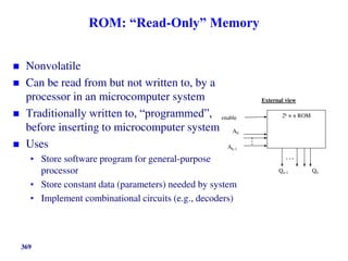
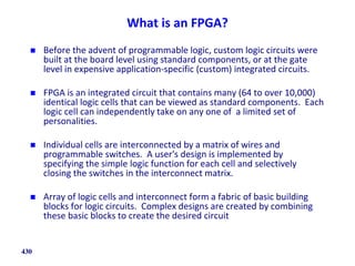
![MOSFET I-V Characteristics
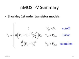
Summary of Analytical Equations
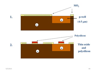
– The voltage directions and relationships for the three
modes of pMOS are in contrast to those of nMOS.
nMOS
Mode ID Voltage Range
Cut-off 0 VGS<VT
Linear (ȝnCox/2)(W/L)[2(VGS-
VT)VDS-VDS
2]
VGSVT,VDS< VGS
-VT
Saturatio
n
(ȝnCox/2)(W/L)(VGS-
VT)2(1+ȜVDS)
VGS VT,VDS
VGS -VT
pMOS
Cut-off 0 VGS>VT
Linear (ȝnCox/2)(W/L)[2(VGS-
VT)VDS-VDS
2]
VGS VT,VDS>
VGS -VT
Saturatio (ȝnCox/2)(W/L)(VGS-
2
VGS VT,VDS
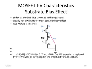
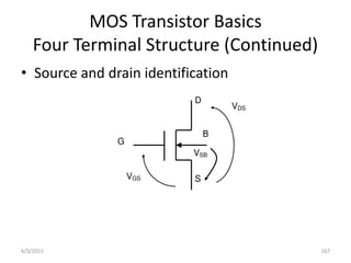
G
D
B
S
VDS
VSB
VGS ID
G
S
B
D
VDS
VSB
VGS
ID
6/3/2015 135](https://image.slidesharecdn.com/vlsippt0-220823022252-91fe5390/85/VLSI-PPT-_0-pdf-133-320.jpg)


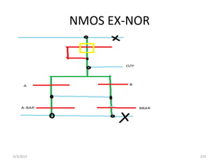
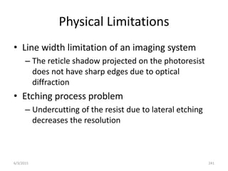
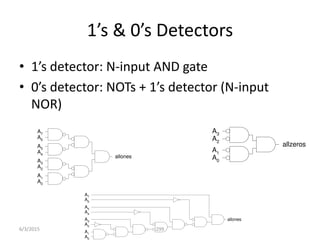
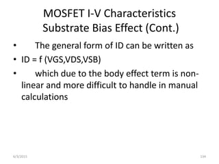
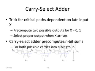
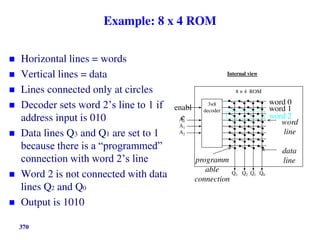
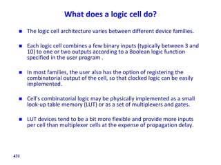
![Equality Comparator
• Check if each bit is equal (XNOR, aka equality
gate)
• s dete t o it ise e ualit
301
A[0]
B[0]
A = B
A[1]
B[1]
A[2]
B[2]
A[3]
B[3]
6/3/2015](https://image.slidesharecdn.com/vlsippt0-220823022252-91fe5390/85/VLSI-PPT-_0-pdf-299-320.jpg)
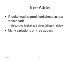
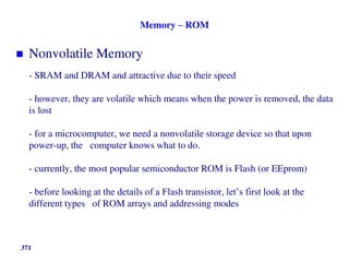

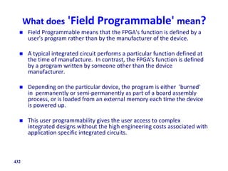

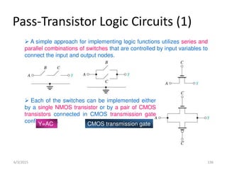
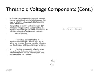
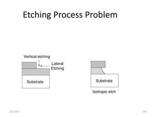
![PRSG
Linear Feedback Shift Register
• Shift register with input taken from XOR of state
• Pseudo-Random Sequence Generator
472
Flop
Flop
Flop
Q[0] Q[1] Q[2]
CLK
D D D
Step Y
0 111
1 110
2 101
3 010
4 100
5 001
6 011
7 111 (repeats)
Flops reset to 111
Y](https://image.slidesharecdn.com/vlsippt0-220823022252-91fe5390/85/VLSI-PPT-_0-pdf-470-320.jpg)
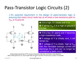
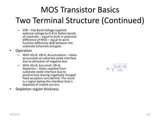
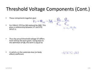
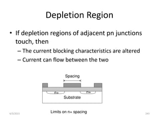
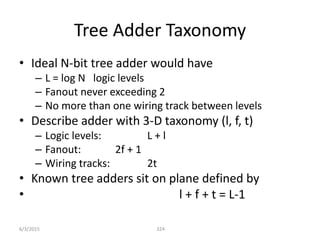
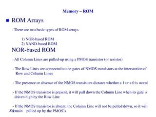
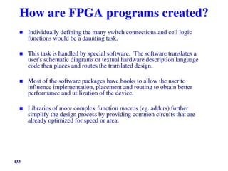
![BILBO
Built-in Logic Block Observer
• Combine scan with PRSG & signature analysis
473
MODE C[1] C[0]
Scan 0 0
Test 0 1
Reset 1 0
Normal 1 1
Flop
Flop
Flop
1
0
D[0] D[1] D[2]
Q[0]
Q[1]
Q[2] / SO
SI
C[1]
C[0]
PRSG
Logic
Cloud
Signature
Analyzer](https://image.slidesharecdn.com/vlsippt0-220823022252-91fe5390/85/VLSI-PPT-_0-pdf-471-320.jpg)