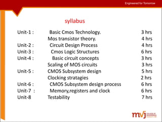
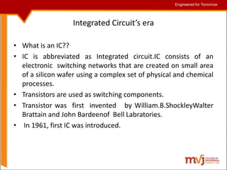
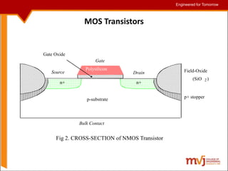
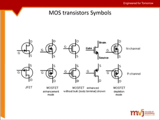
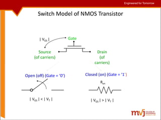
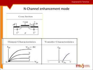
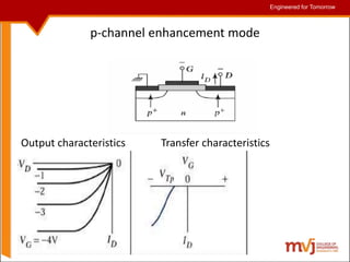
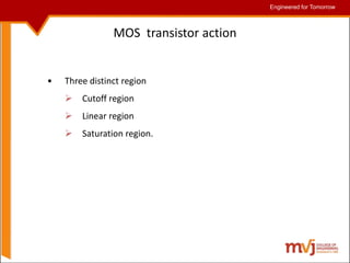
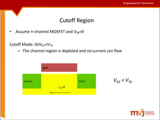
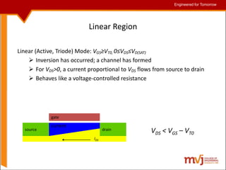
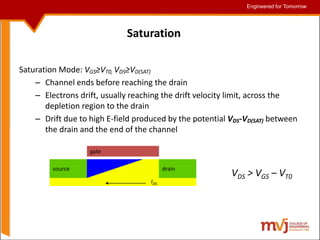
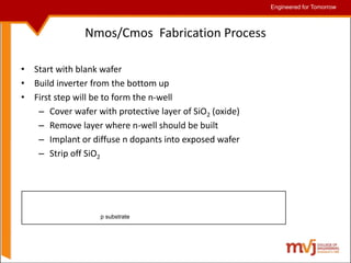
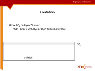
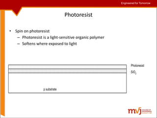
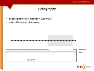
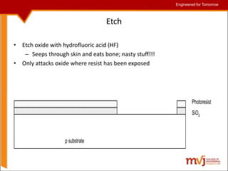
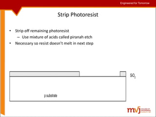
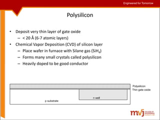
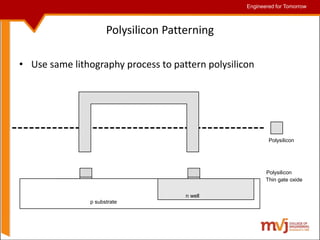
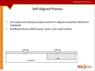
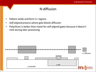
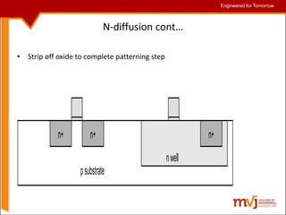
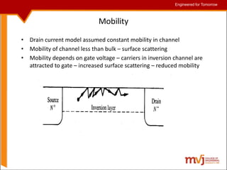
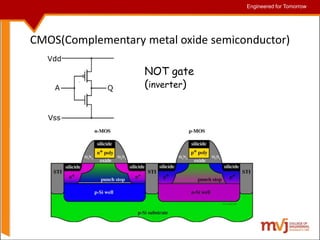
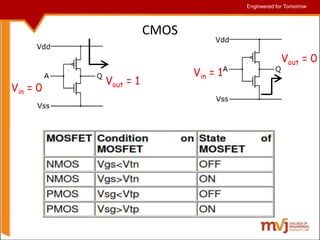
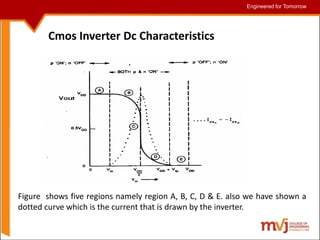
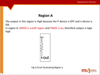
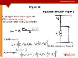
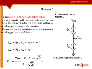
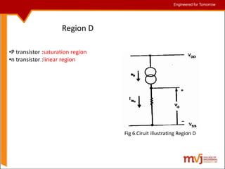
1. Engineered for Tomorrow
Date : 11/10/14
Prepared by : MN PRAPHUL & ASWINI N
Assistant professor
ECE Department
Engineered for Tomorrow
Subject Name: Fundamentals Of CMOS VLSI
Subject Code: 10EC56
Prepared By: Aswini N, Praphul M N
Department: ECE
Date: 10/11/2014
2. Engineered for Tomorrow
Engineered for Tomorrow
syllabus
Unit-1 : Basic Cmos Technology. 3 hrs
Mos transistor theory. 4 hrs
Unit-2 : Circuit Design Process 4 hrs
Unit-3 : Cmos Logic Structures 6 hrs
Unit-4 : Basic circuit concepts 3 hrs
Scaling of MOS circuits 3 hrs
Unit-5 : CMOS Subsystem design 5 hrs
Clocking stratagies 2 hrs
Unit-6 : CMOS Subsystem design process 6 hrs
Unit-7 : Memory,registers and clock 6 hrs
Unit-8 Testability 7 hrs
3. Engineered for Tomorrow
Engineered for Tomorrow
Hello friends!.. you are on a way to understand one of
the most fascinating fields of modern times.Welcome
to the world of VLSI.
5. Engineered for Tomorrow
Engineered for Tomorrow
Syllabus
ďą Integrated Circuitâs era.
ďą Enhancement and Depletion mode MOS transistors.
ďą Nmos Fabrication
ďą CMOS Fabrication.
ďą Thermal aspects of Processing
ďą BICMOS technology
ďą Production of E-beam masks
6. Engineered for Tomorrow
Engineered for Tomorrow
Integrated Circuitâs era
⢠What is an IC??
⢠IC is abbreviated as Integrated circuit.IC consists of an
electronic switching networks that are created on small area
of a silicon wafer using a complex set of physical and chemical
processes.
⢠Transistors are used as switching components.
⢠Transistor was first invented by William.B.ShockleyWalter
Brattain and John Bardeenof Bell Labratories.
⢠In 1961, first IC was introduced.
7. Engineered for Tomorrow
Engineered for Tomorrow
Level of integration Number of transistors Examples
SSI(Small Scale
Integration)
10-100 transistors Logic gates
MSI(Medium Scale
Integration)
100-1000 transistors counters
LSI(Large Scale
Integration)
1000-20000 transistors 8-bit chip
VLSI(Very Large Scale
Integration)
20000-100000
transistors
Example:16 & 32 bit
microprocessors
ULSI(Ultra Large Scale
Integration)
1000000-10000000
transistors
DSPâs, virtual reality
machines, smart
sensors
Levels of transistors integrated
8. Engineered for Tomorrow
Engineered for Tomorrow
Mooreâs Law
âThe number of transistors embedded on the chip doubles after
every one and a half years.â
---Gordon Moore, cofounder Intel Corporation
Fig 1. Moore's graph
10. Engineered for Tomorrow
Engineered for Tomorrow
Metal-oxide semiconductor field-effect transistor (MOSFET) has been
extremely popular since the late 1970s.
Compared to BJTs, MOS transistors:
â˘Can be made smaller /higher integration scale
â˘Easier to fabricate /lower manufacturing cost
â˘Simpler circuitry for digital logic and memory
â˘Inferior analog circuit performance (lower gain)
Most digital ICs use MOS technology
Field-Effect Transistor (FET)
11. Engineered for Tomorrow
Engineered for Tomorrow
MOS Transistors
n+
n+
p-substrate
Field-Oxide
(SiO 2)
p+ stopper
Polysilicon
Gate Oxide
Drain
Source
Gate
Bulk Contact
Fig 2. CROSS-SECTION of NMOS Transistor
13. Engineered for Tomorrow
Engineered for Tomorrow
Switch Model of NMOS Transistor
Gate
Source
(of carriers)
Drain
(of
carriers)
| VGS |
| VGS | < | VT | | VGS | > | VT |
Open (off) (Gate = â0â) Closed (on) (Gate = â1â)
Ron
14. Engineered for Tomorrow
Engineered for Tomorrow
Switch Model of PMOS Transistor
Gate
Source
(of carriers)
Drain
(of carriers)
| VGS |
| VGS | > | VDD â | VT | | | VGS | < | VDD â |VT| |
Open (off) (Gate = â1â) Closed (on) (Gate = â0â)
Ron
15. Engineered for Tomorrow
Engineered for Tomorrow
MOSFETs- Enhancement Type
The enhancement-type NMOS transistor with a positive voltage applied
to the gate. An n channel is induced at the top of the substrate beneath
the gate.
16. Engineered for Tomorrow
Engineered for Tomorrow
Physical Operation of Enhancement MOSFET
â˘If S and D are grounded and a positive
voltage is applied to G, the holes are
repelled from the channel region
downwards, leaving behind a carrier-
depletion region.
â˘Further increasing VG attracts minority
carrier ( electrons) from the substrate into
the channel region.
â˘When sufficient amount of electrons
accumulate near the surface of the
substrate under the gate, an n region is
created-called as the inversion layer.
19. Engineered for Tomorrow
Engineered for Tomorrow
Field-Effect Transistors (FETs) Depletion Type
ďThe depletion type MOSFET has similar structure to that the enhancement
type MOSFET but with one important difference
ďThe depletion MOSFET has a physically implanted channel. Thus an n-channel
depletion-type MOSFET has an n-type silicone region connecting the source and
drain (both +n) at the top of the type substrate.
The channel depth and hence its conductivity is controlled by vGS. Applying a
positive vGS enhances the channel by attracting more electrons. The reverse
when applying negative volt. The negative voltage is said to deplete the channel
(depletion mode).
21. Engineered for Tomorrow
Engineered for Tomorrow
MOS transistor action
⢠Three distinct region
ď Cutoff region
ď Linear region
ď Saturation region.
22. Engineered for Tomorrow
Engineered for Tomorrow
Cutoff Region
⢠Assume n-channel MOSFET and VSB=0
Cutoff Mode: 0â¤VGS<VT0
â The channel region is depleted and no current can flow
gate
drain
source
IDS=0
VGS < VT0
23. Engineered for Tomorrow
Engineered for Tomorrow
Linear Region
Linear (Active, Triode) Mode: VGSâĽVT0, 0â¤VDSâ¤VD(SAT)
ď Inversion has occurred; a channel has formed
ď For VDS>0, a current proportional to VDS flows from source to drain
ď Behaves like a voltage-controlled resistance
gate
drain
source
current
IDS
VDS < VGS â VT0
24. Engineered for Tomorrow
Engineered for Tomorrow
Pinch-Off
Pinch-Off Point (Edge of Saturation) : VGSâĽVT0, VDS=VD(SAT)
â Channel just reaches the drain
â Channel is reduced to zero inversion charge at the drain
â Drifting of electrons through the depletion region between the
channel and drain has begun
gate
drain
source
current
IDS
VDS = VGS â VT0
25. Engineered for Tomorrow
Engineered for Tomorrow
Saturation
Saturation Mode: VGSâĽVT0, VDSâĽVD(SAT)
â Channel ends before reaching the drain
â Electrons drift, usually reaching the drift velocity limit, across the
depletion region to the drain
â Drift due to high E-field produced by the potential VDS-VD(SAT) between
the drain and the end of the channel
gate
drain
source
IDS
VDS > VGS â VT0
26. Engineered for Tomorrow
Engineered for Tomorrow
Nmos/Cmos Fabrication Process
⢠Start with blank wafer
⢠Build inverter from the bottom up
⢠First step will be to form the n-well
â Cover wafer with protective layer of SiO2 (oxide)
â Remove layer where n-well should be built
â Implant or diffuse n dopants into exposed wafer
â Strip off SiO2
p substrate
27. Engineered for Tomorrow
Engineered for Tomorrow
Oxidation
⢠Grow SiO2 on top of Si wafer
â 900 â 1200 C with H2O or O2 in oxidation furnace
p substrate
SiO2
28. Engineered for Tomorrow
Engineered for Tomorrow
Photoresist
⢠Spin on photoresist
â Photoresist is a light-sensitive organic polymer
â Softens where exposed to light
p substrate
SiO2
Photoresist
29. Engineered for Tomorrow
Engineered for Tomorrow
Lithography
⢠Expose photoresist through n-well mask
⢠Strip off exposed photoresist
p substrate
SiO2
Photoresist
30. Engineered for Tomorrow
Engineered for Tomorrow
Etch
⢠Etch oxide with hydrofluoric acid (HF)
â Seeps through skin and eats bone; nasty stuff!!!
⢠Only attacks oxide where resist has been exposed
p substrate
SiO2
Photoresist
31. Engineered for Tomorrow
Engineered for Tomorrow
Strip Photoresist
⢠Strip off remaining photoresist
â Use mixture of acids called piranah etch
⢠Necessary so resist doesnât melt in next step
p substrate
SiO2
32. Engineered for Tomorrow
Engineered for Tomorrow
Polysilicon
⢠Deposit very thin layer of gate oxide
â < 20 Ă (6-7 atomic layers)
⢠Chemical Vapor Deposition (CVD) of silicon layer
â Place wafer in furnace with Silane gas (SiH4)
â Forms many small crystals called polysilicon
â Heavily doped to be good conductor
Thin gate oxide
Polysilicon
p substrate
n well
33. Engineered for Tomorrow
Engineered for Tomorrow
Polysilicon Patterning
⢠Use same lithography process to pattern polysilicon
Polysilicon
p substrate
Thin gate oxide
Polysilicon
n well
34. Engineered for Tomorrow
Engineered for Tomorrow
Self-Aligned Process
⢠Use oxide and masking to expose where n+ dopants should be diffused or
implanted
⢠N-diffusion forms nMOS source, drain, and n-well contact
p substrate
n well
35. Engineered for Tomorrow
Engineered for Tomorrow
N-diffusion
⢠Pattern oxide and form n+ regions
⢠Self-aligned process where gate blocks diffusion
⢠Polysilicon is better than metal for self-aligned gates because it doesnât
melt during later processing
n+ Diffusion
p substrate
n well
36. Engineered for Tomorrow
Engineered for Tomorrow
N-diffusion contâŚ
⢠Strip off oxide to complete patterning step
nwell
psubstrate
n+
n+ n+
37. Engineered for Tomorrow
Engineered for Tomorrow
P-Diffusion
⢠Similar set of steps form p+ diffusion regions for pMOS source and drain
and substrate contact
p+ Diffusion
p substrate
n well
n+
n+ n+
p+
p+
p+
38. Engineered for Tomorrow
Engineered for Tomorrow
Contacts
⢠Now we need to wire together the devices
⢠Cover chip with thick field oxide
⢠Etch oxide where contact cuts are needed
Contact
p substrate
Thick field oxide
n well
n+
n+ n+
p+
p+
p+
39. Engineered for Tomorrow
Engineered for Tomorrow
Metallization
⢠Sputter on aluminum over whole wafer
⢠Pattern to remove excess metal, leaving wires
Metal
p substrate
Metal
Thick field oxide
n well
n+
n+ n+
p+
p+
p+
40. Engineered for Tomorrow
Engineered for Tomorrow
Bicmos technology
â˘BiCMOS' is an evolved semiconductor technology that integrates two formerly
separate semiconductor technologies - those of the bipolar junction transistor
and the CMOS transistor - in a single integrated circuit device.
â˘Bipolar junction transistors offer high speed, high gain, and low output
resistance, which are excellent properties for high-frequency analog amplifiers.
⢠CMOS technology offers high input resistance and is excellent for constructing
simple, low-power logic gates.
43. Engineered for Tomorrow
Engineered for Tomorrow
Threshold voltage (Vt)
The voltage at which an MOS device begins to conduct ("turn on") is a threshold
voltage. The threshold voltage is a function of following parameters:
ďGate conductor material
ďGate insulator material
ďGate insulator thickness
ďImpurity at the silicon-insulator interface
ďVoltage between the source and the substrate Vsb
ď Temperature
44. Engineered for Tomorrow
Engineered for Tomorrow
Sub-Threshold Behavior
⢠For gate voltage less than the threshold â weak inversion
⢠Diffusion is dominant current mechanism (not drift)
ď¨ ďŠ kT
q
kT
qV
kT
i
n
D
s
D
B
e
e
L
e
n
qAD
I /
/
/
1 ďš
ď
ďš
ď
ď
ď˝
â˘Sub-threshold current is exponential function of applied gate voltage
â˘Sub-threshold current gets larger for smaller gates (L)
45. Engineered for Tomorrow
Engineered for Tomorrow
Channel Length Modulation
ď With pinch-off the channel at the point y such that Vc(y)=VGS - VT0, The
effective channel length is equal to Lâ = L â ÎL
ÎL is the length of channel segment over which QI=0.
ď Place Lâ in the ID(SAT) equation:
2
0
)
( )
(
2
V
V
L
W
C
I T
GS
ox
n
SAT
D ď
ď˘
ď˝
ď
Fig2 .Illustrating channel length modulation
46. Engineered for Tomorrow
Engineered for Tomorrow
Mobility
⢠Drain current model assumed constant mobility in channel
⢠Mobility of channel less than bulk â surface scattering
⢠Mobility depends on gate voltage â carriers in inversion channel are
attracted to gate â increased surface scattering â reduced mobility
47. Engineered for Tomorrow
Engineered for Tomorrow
Drain punch through
â˘Punch through in a MOSFET is an extreme case of channel length modulation
where the depletion layers around the drain and source regions merge into a
single depletion region.
â˘The field underneath the gate then becomes strongly dependent on the drain-
source voltage, as is the drain current.
â˘Punch through causes a rapidly increasing current with increasing drain-source
voltage.
â˘This effect is undesirable as it increases the output conductance and limits the
maximum operating voltage of the device
50. Engineered for Tomorrow
Engineered for Tomorrow
Cmos Inverter Dc Characteristics
Figure shows five regions namely region A, B, C, D & E. also we have shown a
dotted curve which is the current that is drawn by the inverter.
51. Engineered for Tomorrow
Engineered for Tomorrow
The output in this region is High because the P device is OFF and n device is
ON.
In region A, NMOS is cutoff region and PMOS is on, therefore output is logic
high.
Region A
Fig 3.Ciruit illustrating Region a
52. Engineered for Tomorrow
Engineered for Tomorrow
Region B:
In this region PMOS :linear region and
NMOS: saturation region.
The expression for the NMOS current is
Equivalent circuit in Region B
PMOS current is
Output voltage is
Fig 4.Ciruit illustrating Region B
53. Engineered for Tomorrow
Engineered for Tomorrow
Region C:
â˘Both n and p transistors :saturation region.
â˘we can equate both the currents and we can
obtain the expression for the mid point voltage or
switching point voltage of a inverter.
â˘The corresponding equations for nmos, pmos and
switching point are as follows:
Equivalent circuit in
Region C
Fig 5.Ciruit illustrating Region C
54. Engineered for Tomorrow
Engineered for Tomorrow
Region D
â˘P transistor :saturation region
â˘n transistor :linear region
Fig 6.Ciruit illustrating Region D
55. Engineered for Tomorrow
Engineered for Tomorrow
7.1.5 Region E:
The output in this region is zero.
P device :OFF and n device : ON.
Fig 7.Ciruit illustrating Region E
56. Engineered for Tomorrow
Engineered for Tomorrow
Influence of Ăn/Ăp on the VTC characteristics:
The characteristics shifts left if the ratio of
Ăn/Ăp is greater than 1(say 10). The curve
shifts right if the ratio of Ăn/Ăp is lesser
than 1(say 0.1).
57. Engineered for Tomorrow
Engineered for Tomorrow
â˘Noise margin is a parameter related to
input output characteristics.
â˘It determines the allowable noise
voltage on the input so that the output is
not affected. We will specify it in terms of
two things:
ďLOW noise margin NM L =|VILmax â
VOLmax|
ďHIGH noise margin NMH=|Vohmin â
VIHmin|
Noise Margin:
58. Engineered for Tomorrow
Engineered for Tomorrow
Static Load MOS inverters
This circuit uses a resistive load and current source load inverter. Usually resistive
load inverters are not preferred because of the power consumption and area issues.
59. Engineered for Tomorrow
Engineered for Tomorrow
Pseudo-NMOS inverter:
This circuit uses the load device which is p device and is made to turn on always
by connecting the gate terminal to the ground.
Power consumption is High compared to CMOS inverter particularly when NMOS
device is ON because the p load device is always ON.
60. Engineered for Tomorrow
Engineered for Tomorrow
Saturated load inverter:
â˘The load device is an nMOS transistor in the saturated load inverter.
â˘This type of inverter was used in nMOS technologies prior to the availability of
nMOS depletion loads.
62. Engineered for Tomorrow
Engineered for Tomorrow
Transmission gates(TGs)
Itâs a parallel combination of pmos and nmos transistor with the gates connected
to a complementary input. The disadvantages weak 0 and weak 1 can be overcome
by using a TG instead of pass transistors.
When
¢=â0â n and p device off, Vin=0 or 1, Vo=âZâ
When
¢=â1â n and p device on, Vin=0 or 1, Vo=0 or 1 , where âZâ is high
impedance.
63. Engineered for Tomorrow
Engineered for Tomorrow
Tristate Inverter:
By cascading a transmission gate with an inverter the tristate inverter circuit
can be obtained. The working can be explained with the help of the circuit.
The two circuits are the same only difference is the way they are written.
When CL is zero the output of the inverter is in tristate condition. When CL is
high the output is Z is the inversion of the input A