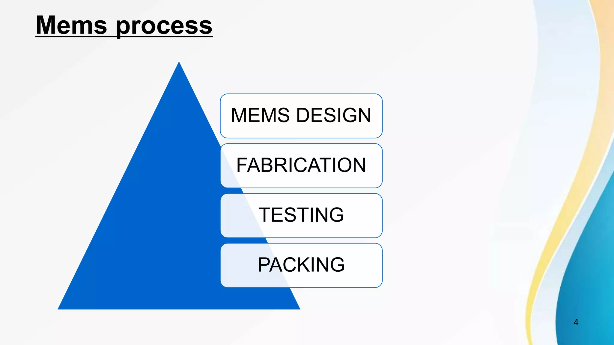
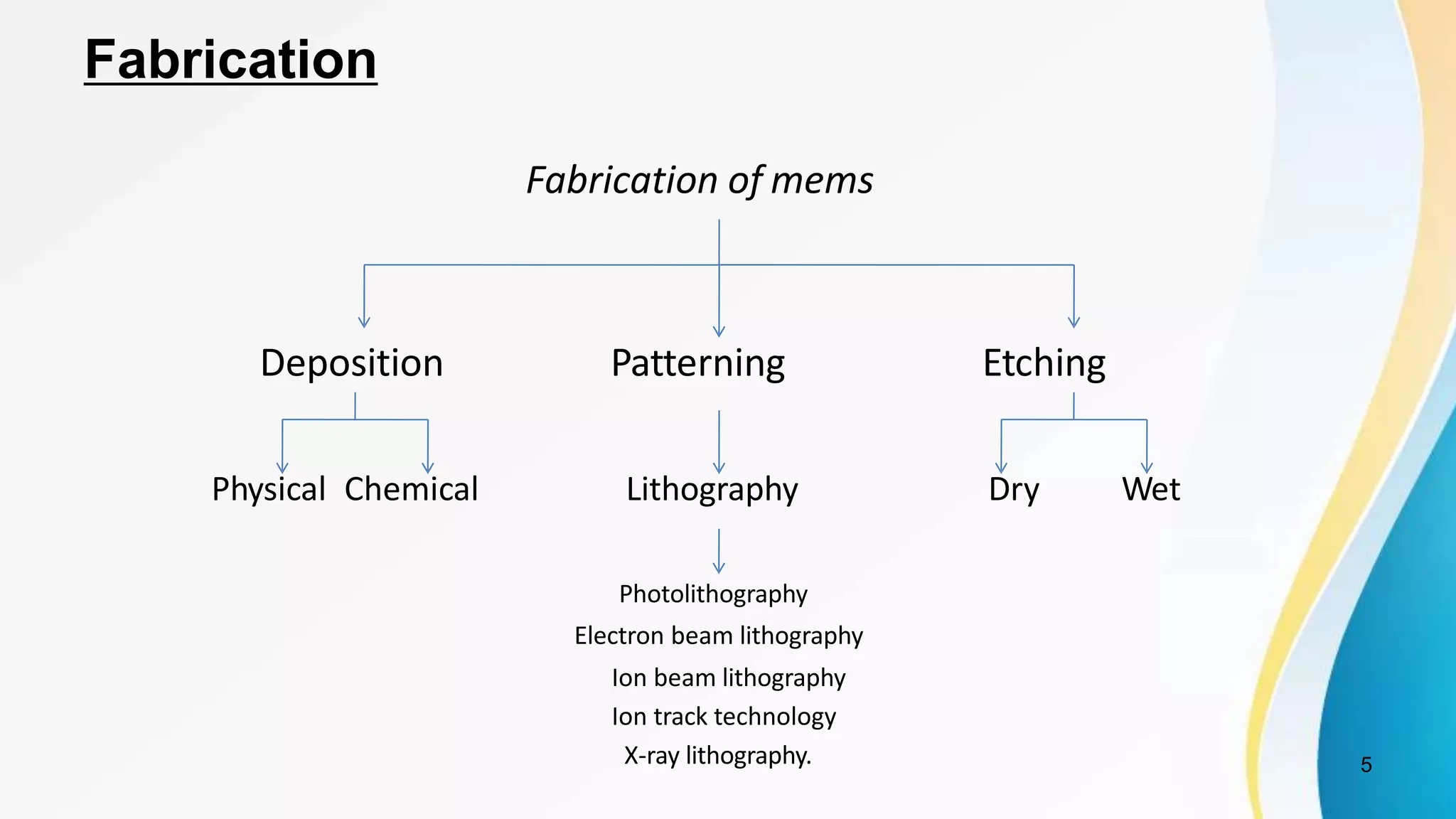
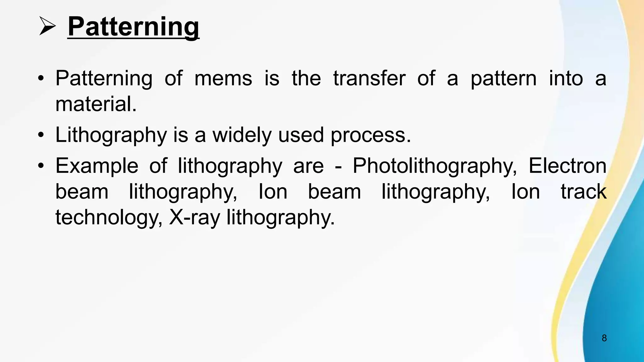
Swami Keshvanand Institute of Technology M & G
JAIPUR
Supervisor:-
Mr. Trivendra Sharma
Submitted to :
Mr. Dinesh Kumar Sharma
Mr. Ankit Agarwal
Submitted By:
Govind Ram Kumawat
15ESKME052
Sec. A VIII sem
1
CONTENTS
• Introduction
• Mems process
• Fabrication
• Materials for mems
• Application of mems
• Advantages and Disadvantages
• Conclusion
• Reference
2
Introduction
• Micro electro mechanical system is a technology of very small
devices.
• It is a combination of a mechanical function (sensing, moving,
heating) and electrical function (switching, deciding) on the
same chip using micro fabrication technology.
• MEMS are made up of components between 1 to 100 micro
meter in size.
• MEMS devices generally range in size from 20 micrometer to a
millimeter.
3
Mems process
MEMS DESIGN
FABRICATION
TESTING
PACKING
4
Fabrication
Fabrication of mems
Deposition Patterning Etching
Physical Chemical Lithography Dry Wet
Photolithography
Electron beam lithography
Ion beam lithography
Ion track technology
X-ray lithography. 5
Fabrication Process
Fig. 1 : Fabrication Process 6
 Deposition
1. Physical Deposition: Physical deposition consists of a
process in which a material is removed from a target and
deposited on a surface.
2. Chemical Deposition: Chemical deposition techniques
include chemical vapor deposition in which a stress of
source gas reacts on the substrate to grow the material
desired.
7
 Patterning
• Patterning of mems is the transfer of a pattern into a
material.
• Lithography is a widely used process.
• Example of lithography are - Photolithography, Electron
beam lithography, Ion beam lithography, Ion track
technology, X-ray lithography.
8
Cont...
Fig. 2: Patterning 9
Etching
• Etching is the process of using strong acid to cut the
unprotected parts of a metal surface to create a design in.
• There are to classes of etching processes:
1. Wet Etching.
2. Dry Etching.
Fig. 3 : Etching
10
Materials for mems
• Materials are the basic things required to develop micro
sensors.
• Metals
• Polymers
• Ceramic materials
• Semiconductors
• Composite materials
11
Application of mems
1. In Medical Field:
• A MEMS device can be
implanted in the human
body.
• MEMS surgical tools
provide the flexibility and
accuracy to perform
surgery.
12
2. In Automotives:
• Air bag system.
• Vehicle security system.
• Inertial brake lights.
• Rollover detection.
• Automatic door locks.
3. As Gyroscope
4. In Microphone
5. As Sensors
13
6. In Accelerometers:
MEMS accelerometers are widely used in
• Cars for airbad deployment.
• Smart phone.
• Gaming devices for sensing motion.
14
Advantages of mems
• Minimize energy and materials used in manufacturing.
• Improved reproducibility.
• Improved accuracy and reliability.
• Increased selectivity and sensitivity.
• Cost and performance advantage.
• Very small size, mass, volume.
• Very low power consumption.
15
Disadvantages of mems
• Very complex design procedure.
• Micro-component are costly compared to the macro
components.
• Farm establishment requires huge investments.
16
Conclusion
• MEMS promises to be an effective technique of producing
sensors of high quality, at lower costs.
• This enabling technology promises to create entirely new
categories of products.
• MEMS will be the indispensible factor in advancing
technology.
17
Reference
18
THANK YOU !
19

Micro Electro Mechanical System

  • 1.
    Swami Keshvanand Instituteof Technology M & G JAIPUR Supervisor:- Mr. Trivendra Sharma Submitted to : Mr. Dinesh Kumar Sharma Mr. Ankit Agarwal Submitted By: Govind Ram Kumawat 15ESKME052 Sec. A VIII sem 1
  • 2.
    CONTENTS • Introduction • Memsprocess • Fabrication • Materials for mems • Application of mems • Advantages and Disadvantages • Conclusion • Reference 2
  • 3.
    Introduction • Micro electromechanical system is a technology of very small devices. • It is a combination of a mechanical function (sensing, moving, heating) and electrical function (switching, deciding) on the same chip using micro fabrication technology. • MEMS are made up of components between 1 to 100 micro meter in size. • MEMS devices generally range in size from 20 micrometer to a millimeter. 3
  • 4.
  • 5.
    Fabrication Fabrication of mems DepositionPatterning Etching Physical Chemical Lithography Dry Wet Photolithography Electron beam lithography Ion beam lithography Ion track technology X-ray lithography. 5
  • 6.
    Fabrication Process Fig. 1: Fabrication Process 6
  • 7.
     Deposition 1. PhysicalDeposition: Physical deposition consists of a process in which a material is removed from a target and deposited on a surface. 2. Chemical Deposition: Chemical deposition techniques include chemical vapor deposition in which a stress of source gas reacts on the substrate to grow the material desired. 7
  • 8.
     Patterning • Patterningof mems is the transfer of a pattern into a material. • Lithography is a widely used process. • Example of lithography are - Photolithography, Electron beam lithography, Ion beam lithography, Ion track technology, X-ray lithography. 8
  • 9.
  • 10.
    Etching • Etching isthe process of using strong acid to cut the unprotected parts of a metal surface to create a design in. • There are to classes of etching processes: 1. Wet Etching. 2. Dry Etching. Fig. 3 : Etching 10
  • 11.
    Materials for mems •Materials are the basic things required to develop micro sensors. • Metals • Polymers • Ceramic materials • Semiconductors • Composite materials 11
  • 12.
    Application of mems 1.In Medical Field: • A MEMS device can be implanted in the human body. • MEMS surgical tools provide the flexibility and accuracy to perform surgery. 12
  • 13.
    2. In Automotives: •Air bag system. • Vehicle security system. • Inertial brake lights. • Rollover detection. • Automatic door locks. 3. As Gyroscope 4. In Microphone 5. As Sensors 13
  • 14.
    6. In Accelerometers: MEMSaccelerometers are widely used in • Cars for airbad deployment. • Smart phone. • Gaming devices for sensing motion. 14
  • 15.
    Advantages of mems •Minimize energy and materials used in manufacturing. • Improved reproducibility. • Improved accuracy and reliability. • Increased selectivity and sensitivity. • Cost and performance advantage. • Very small size, mass, volume. • Very low power consumption. 15
  • 16.
    Disadvantages of mems •Very complex design procedure. • Micro-component are costly compared to the macro components. • Farm establishment requires huge investments. 16
  • 17.
    Conclusion • MEMS promisesto be an effective technique of producing sensors of high quality, at lower costs. • This enabling technology promises to create entirely new categories of products. • MEMS will be the indispensible factor in advancing technology. 17
  • 18.
  • 19.